Narendra Yadava, Shivangi Mani, and R. K. Chauhan
Abstract
The radio-frequency (RF) performance of the p-type NiO-pocket based β-Ga2O3/black phosphorous heterostructure MOSFET has been evaluated. The key figure of merits (FOMs) for device performance evaluation include the transconductance (gm) gate dependent intrinsic-capacitances (Cgd and Cgs), cutoff frequency (fT), gain bandwidth (GBW) product and output-conductance (gd). Similarly, power-gain (Gp), power added efficiency (PAE), and output power (POUT) are also investigated for large-signal continuous-wave (CW) RF performance evaluation. The motive behind the study is to improve the β-Ga2O3 MOS device performance along with a reduction in power losses and device associated leakages. To show the applicability of the designed device in RF applications, its RF FOMs are analyzed. With the outline characteristics of the ultrathin black phosphorous layer below the β-Ga2O3 channel region, the proposed device results in 1.09 times improvement in fT, with 0.7 times lower Cgs, and 3.27 dB improved GP in comparison to the NiO-GO MOSFET. The results indicate that the designed NiO-GO/BP MOSFET has better RF performance with improved power gain and low leakages.1. Introduction
The demand for high-performance, compact, and battery-operated devices for RF applications leads to the need for technology where power losses should be low[1]. To reduce the losses associated with the RF power devices, silicon material needs to be replaced by the other semiconductor material because the devices based on this technology are reaching their theoretical limits[2]. To compensate for several limitations found in Si-based devices, wide bandgap (WBG) semiconductors like GaN (~3.4 eV) and SiC (~3.3 eV) became the favorable materials to be opted[3]. In high power applications, the devices based on WBG (i.e GaN & SiC) semiconductor materials show the excellent capability of withstanding high breakdown voltage ( Vbr) with reduced power losses and leakages in comparison to Si[4]. However, for efficient implementation of high-power RF amplifiers with stable high-temperature operation certain parameters such as RON, off-state leakage current, switching speed, and Vbr, need to be optimized[5].
As a power electronics semiconductor, β-Ga2O3 has emerged in several fields from very high voltage power switching[5-7] to even GHz RF power amplification[8]. This is due to the advantage of high theoretical critical field strength (Ec) that surpasses both the SiC and GaN Ec values[9]. The two important high-frequency power device figure-of-merits (FOMs); i.e., the Johnson (2844.4) and Baliga’s (3214.1) FOMs are found to be exceptionally high for Ga2O3 concerning silicon[10]. With its mobility ranging as 100 cm2/(V·s), β-Ga2O3 transistors trend an opportunity towards operating as amplifiers that can be used for RF applications; i.e., RF amplifiers, RF switches and many more[5, 8].
In RF and power electronic applications based on gallium oxide MOS technology, several types of research have been carried out[3-10]. Mastro et al. discloses the reference to further opportunities in space of Ga2O3 and formulated a study that depicts Ga2O3 possess high electron saturation velocity (vsat) along with high output current density, which gives a high value of cut-off frequency[10]. Further, Higashiwaki et al. demonstrates the performance of gallium oxide MOSFET under depletion mode operating condition and observed that 2 μm of gate length MOS device result in minimum off-state leakage current with ION/IOFF ratio greater than 1010[4]. Green et al. diverted the further study of gallium oxide MOSFET towards RF performance and stated its high value of gm (21 mS/mm) and fT (3.3 GHz)[8].
As 2D material technologies emerge in the space for future electronic devices, black phosphorous (BP) and also graphene have become rewarding materials. Recently, due to excellent electron transport properties, graphene has been the main focus for future RF electronics[11]. Being considered as a gapless semiconductor, graphene has an advantage of higher carrier mobility even at room temperature, which adds that β-Ga2O3 quite compatible with it. However, due to its poor saturation behavior, the use of graphene in RF and switching applications is still limited.
BP has been considered as another tunable bandgap material[12] with its higher carrier mobility stated as 1000 cm2/(V·s). Due to the improved saturation behavior property, BP is particularly suited as an alternative for graphene[11, 13]. Li et al. fabricated FET based upon BP crystals with thickness referring to few nanometers. Reliability in these devices was observed at room temperature with 7.5 nm thickness and drain current modulation of 105 results in a better I–V characteristic[14]. Yan et al. studied the performance of β-Ga2O3/graphene heterostructure in a vertical barristor. The fabricated structure results in a high breakdown field of ~5 MV/cm and was found to be close to the theoretical Ec of β-Ga2O3 (~8 MV/cm)[15]. A comprehensive study for analog and RF performance of BP (20 nm) based MOSFET was analyzed by Kumar et al.[16]. The figure of merits investigated was –fT, fmax, stern stability factor, various power gains along with parasitic capacitances at THz frequency range. The results show that the designed device is more suitable for RF applications. Yadava and Chauhan insights the introduction of a single layer of graphene/BP in Ga2O3 MOSFET to improve its RF performance. The losses associated with the introduction of the BP layer in Ga2O3 MOSFET has not been discussed in the above work[17]. But the problem lied in the β-Ga2O3 doping profile as the lack of p-type doping on β-Ga2O3 limits certain operations. Usually, for growing β-Ga2O3 single crystals and thin films, n-type was considered because their existence of unmeant impurities[18].
To overcome the lack of p-type conductivity in Ga2O3, p-type oxide (like Ir2O3, NiO) based heterostructures were considered[19]. Usage of the MOSFET with p-type Ir2O3 oxide-based channel region was demonstrated by FLOSFIA Inc.[20], which is considered as a groundbreaking work for future high-power electronics devices. Kokunan et al. fabricated the NiO/Ga2O3 hetero-junction diode by growing the p-type NiO layer on the Ga2O3 substrate using the sol-gel technique. The fabricated devices showed good rectifying behavior with a ratio >10 8 at ± 3.0 V[21]. The RF performance investigation of NiO (p-type) pocket based Ga2O3 MOSFET was done by Yadava and Chauhan, where the capacitance Cgs, which has a direct correlation with the device leakage, decreases with the use of NiO pocket region at both of the channel interfaces[22].
This paper investigates the impact of the BP layer on the RF performance of NiO pocket based gallium oxide MOSFET. The key FOMs for device performance evaluation includes the transconductance (gm), gate dependent intrinsic-capacitances (Cgd and Cgs), cutoff frequency (fT), gain bandwidth (GBW) product and output-conductance (gd). Similarly, power-gain (Gp), power added efficiency (PAE), and output power (POUT) are also investigated for large-signal continuous-wave (CW) RF performance evaluation.
2. Device description
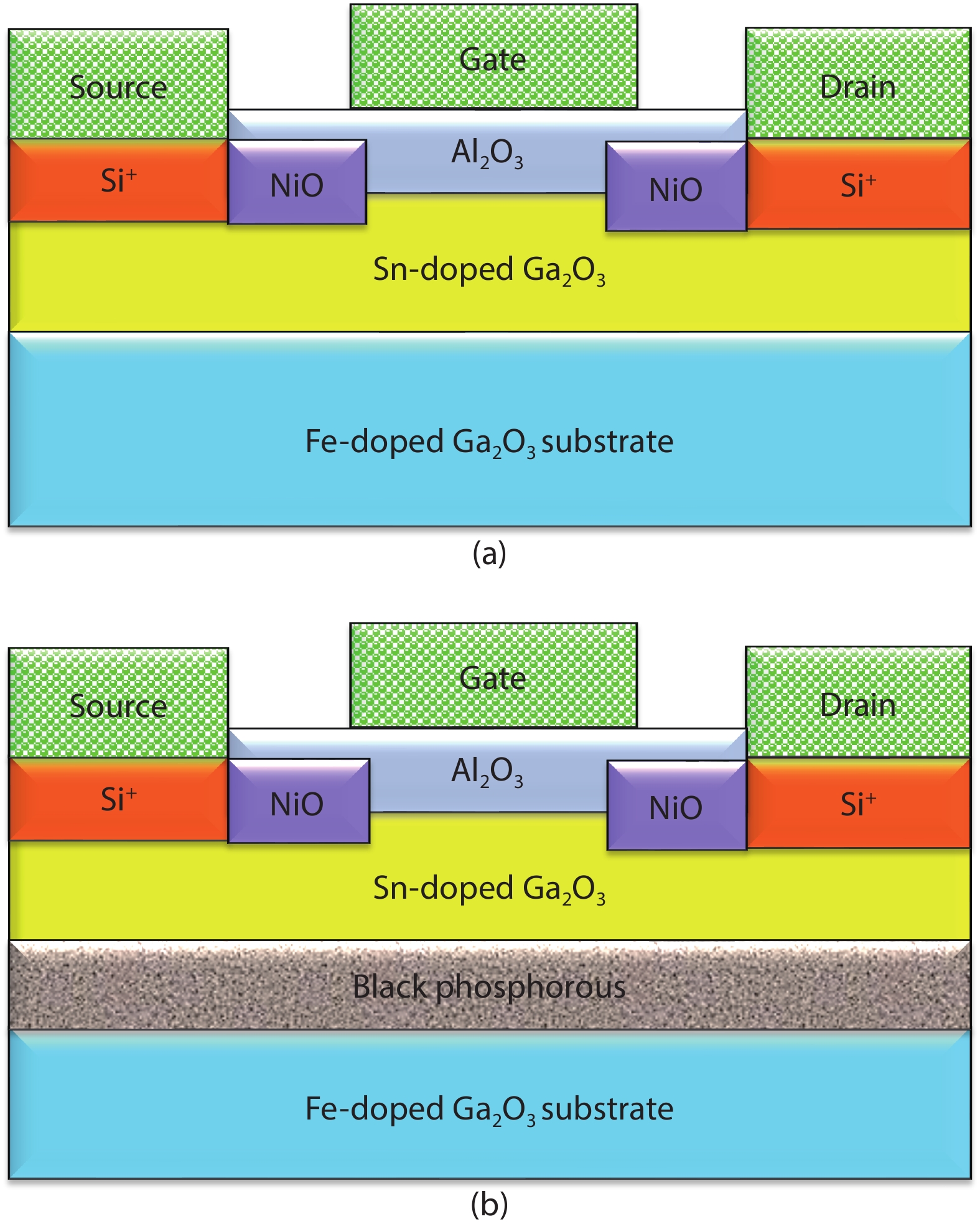
The structures of p-type NiO-pocket based β-Ga2O3 and p-type NiO-pocket based β-Ga2O3/black phosphorous heterostructure MOSFETs are shown in Figs. 1(a) and 1(b), respectively. Figs. 2(a) and 2(b) depicts the lattice temperature of conventional and p-type NiO-pocket based MOSFETs obtained at VDS = + 40 V and VGS = + 4 V. In β-Ga2O3 MOSFET shown in Fig 2(a), the maximum value of lattice temperature reaches to ~ 422 °C. However, with the use of p-type NiO-pocket in the device and under the similar device operating conditions, it only reaches 400 °C. Similarly, Figs. 3(a) and 3(b) shows the potential distribution of conventional and p-type NiO-pocket based MOSFETs respectively. In Fig. 3(b), the use of p-type NiO-pocket at both the channel interfaces results in a minute decrease in the potential is observed. This decrease is due to the abrupt transition in the device impurity doping profile from Ga2O3 (n-type) channel to NiO-pocket (p-type) regions. In the device, a 300 nm thick n-type β-Ga2O3 channel region was made to grow on a single crystal of β-Ga2O3 substrate. The n-type impurity doping concentration of the channel region is ~7 × 1017 cm–3 and around half of this is assumed to be activated by considering the measured C–V data of the fabricated gallium oxide MOS device[4]. The formation of source and drain electrodes is carried out by utilizing multiple Si+ implants with a 150 nm deep box profile of n-type having a doping concentration of 3 × 1019 cm–3 optimized from the collective data of the device[4].

Figure 1.(Color online) (a) P-type NiO-pocket based β-Ga2O3 MOSFET. (b) P-type NiO-pocket based β-Ga2O3/black phosphorous heterostructure MOSFET.
Figure 2.(Color online) Lattice temperature in (a) β-Ga2O3 MOSFET and (b) P-type NiO-pocket based β-Ga2O3 MOSFET.
Figure 3.(Color online) Potential distribution in (a) β-Ga2O3 MOSFET and (b) P-type NiO-pocket based β-Ga2O3 MOSFET.
The overall distance between the source and drain region was 20 µm. On the top of the channel region, a 20 nm thick Al2O3 layer was made to deposited as a gate dielectric layer accompanied by the deposition of 2 µm long Ti/Pt/Au metal gate on the top. In NiO-pocket based β-Ga2O3/BP heterostructure MOSFET, a BP layer of 10 nm thick was made to deposited over the substrate, while keeping other conditions similar. The important material parameters used in the design of the β-Ga2O3/BP heterostructure MOS device are summarized in Table 1.
Table Infomation Is Not Enable
3. Simulation and model calibration method
All the parameters and RF FOMs are extracted out from the ATLAS device simulation tool[23]. The Newton numerical technique is used to obtain numerical solutions because it provides better convergence. For obtaining in the device LAT.TEMP parameter is set up in the model parameter. Using equation (1), we can attain temperature-dependent electron mobility with lattice temperature coefficient TMUN = 2[23]. Along with the ATLAS simulation tool, ATHENA (process simulator) is also used to pro-create multiple Si+ implantations[4] using a material implant model called BCA.
$
{{{\mu}} }_{{\rm{n}}0}={\rm{MUN}}{\left(\frac{{T}_{\rm{L}}}{300}\right)}^{-\rm{TMUN}},
$
(1)
where μn0 is low field mobility, MUN is the electron mobility and TL is lattice temperature.
In the material parameters of the BP region (see Table 1), the bandgap (Eg) is set to 1.88 eV, the relative permittivity and electron affinity of 6.1 and 5.5 eV are taken, respectively. These parameters are obtained from the experimental measurement of the BP FET given by Li et al.[14].
4. Feasible fabrication steps of the devices
The fabrication of the gallium oxide MOSFET was already demonstrated by Higashiwaki et al.[4] and Zing et al.[24]. In the initial fabrication step, a single-crystal of the β-Ga2O3 substrate is made to doped with Fe, over which an Sn doped 300 nm thick n-Ga2O3 channel layer was formed by using the MBE technique[4]. Using Knudsen cells, Sn and Ga fluxes are carried out by powdered SnO2 and Ga metal, respectively. Followed by growing of the SiO2 layer using PECVD[4, 6]. To open up, source, and drain regions, lithography is being performed. Generally, to carry out these fabrication steps, often positive PR along with maskless lithography is used[25]. Using multiple Si+ implantations, source, and drain electrode regions are defined accompanied by annealing[25]. Thereafter, two NiO pocket regions of 10 nm thicker in length were made to form at the channel (drain/channel & source/channel) interfaces. Now, the grown NiO region is made p-type (impurity concentration ~1.6 × 10 17 cm–3) by adding Li as an acceptor impurity[21]. After this, the removal of the deposited SiO2 on the gate region was done by using RIE[4]. Now, the ALD technique is utilization for the deposition of Al2O3 of 20 nm thick as a gate dielectric layer followed by RIE[25, 26]. Soon after the fourth lithography, a 2 µm long Ti/Pt/Au metal gate is formed over the top of the gate oxide layer[4, 25]. For both Ga2O3/BP and p-type NiO pocket based β-Ga2O3/BP heterostructure MOSFETs, a process step is maintained soon after Ga2O3 substrate formation. For this process step, the PDMS stamping technique is used to deposit a thin layer of BP over the substrate layer followed by epitaxial growth of the channel region[16, 17].
5. Results and discussion
To examine RF performance of the devices, the FOMs such as transconductance (gm) gate dependent intrinsic-capacitances (Cgd and Cgs), cutoff frequency (fT), gain bandwidth (GBW) product and output-conductance (gd) are used. All of the analysis is done by using ATLAS 2D simulator[23].
Fig. 4 shows the DC transfer characteristics of simulated devices, to consider the effect of NiO pocket on β-Ga2O3 MOSFET with the BP layer. The transfer and the output characteristics of the devices are shown in Figs. 4 and 5, respectively, in which the conventional device is taken from the reported literature and is very much in agreement with the experimental device demonstrated by Higashiwaki et al.[4].
Figure 4.(Color online) Transfer (ID–VGS) and transconductance (gm) behavior of the devices. Inset: ID–VGS in log-scale.
Figure 5.(Color online) Output characteristics (ID–VDS) of the devices.
In Fig. 4, the increased carrier to carrier scattering at the channel interfaces results in a small increase in the value of drain current (ID) in p-type NiO pocket based Ga2O3 (NiO-GO)[22] MOSFET in comparison to the Conventional Ga2O3 MOSFET (Conv. GO)[17], experimental Ga2O3 MOSFET (Exp.)[4] and β-Ga2O3/BP (GO/BP) heterostructure MOSFET. For the devices, the value of the Ion/Ioff ratio of about 1 × 10¹⁰ is observed with off-state leakage in the range of a few pA.
Fig. 6 shows the output conductance characteristics of the device plotted between gd and VDS with VGS = –4 V. For high gain applications, a device should possess a lower value of gd which can be seen in p-type NiO β-Ga2O3/BP (NiO-GO/BP) heterostructure MOSFET. For a device to be used for RF applications, higher output gain requires lower output conductance as depicted in Eq. (3).
Figure 6.(Color online) Output conductance (gd) behavior of the devices.
By performing small-signal AC analysis after the post-processing operation of DC results, one can obtain the device Cgd and Cgs values at the constant frequency of 0.8 GHz using DC gate voltage swept from –25 to 4 V. Figs. 7 and 8 represent the variation in Cgd and Cgs for different VGS values, respectively. The increased capacitive coupling between the gate and drain terminals of the NiO-GO[22] and NiO-GO/BP MOSFETs results in larger Cgd value in comparison with Conv. GO MOSFET[17]. However, the Cgs value which straightly contributes to the leakage is found to be 0.7 times lesser for NiO-GO/BP MOSFET on comparing to NiO-GO[22] MOSFET.
Figure 7.(Color online) Intrinsic capacitance (Cgs) versus gate voltage (VGS). Inset: fT versus VGS.
Figure 8.(Color online) Intrinsic capacitance (Cgd) versus gate voltage (VGS). Inset: GBW versus VGS.
$
{g}_{\rm{m}}=\frac{\partial {I}_{\rm{D}}}{\partial {V}_{\rm{GS}}},
$
(2)
$
{g}_{\rm{d}}=\frac{\partial {I}_{\rm{D}}}{\partial {V}_{\rm{DS}}},
$
(3)
$
{f}_{\rm{T}}\approx \frac{{g}_{\rm{m}}}{2{{\pi }}({C}_{\rm{gs}}+{C}_{\rm{gd}})},
$
(4)
$
{\rm{GBW}} =\frac{{g}_{\rm{m}}}{2\pi \times 10\times {C}_{\rm{gd}}},
$
(5)
$
{f}_{\rm{T}}={f}_{0}\cdot\left|{H}_{21}\right|.
$
(6)
The fT (see Eq. (4)) is the key FOMs for the depiction of the high-frequency performance of RF devices. The cutoff frequency also stated as GBW (see Eq. (5)) is simultaneously related to H21 (short-circuit current gain). Regarding the two-port network, H21 is known as the ratio of output terminal current to the input terminal current of small-signal with output short-circuited. This parameter is frequency-dependent and its magnitude sweeps at high frequencies with a slope of –20 dB/dec. Keeping this justification, fT can be termed as the frequency value at which the magnitude of H21 decreases to unity. Using Eq. (6) we can evaluate the fT and inset of Fig. 7 shows the fT curve of the proposed device. A smaller value of fT is observed in the case of NiO-GO[22] and NiO-GO/BP MOSFETs in comparison to the Con. GO[17]. However, a 1.09 times improvement in the value of fT is found in NiO-GO/BP MOSFET in comparison to NiO-GO[22] MOSFET.
In Fig. 8, the inset graph indicates that the GBW product decreases with the use of the NiO pocket region of p-type in the device. This is due to the decreased value of gm. However, to compensate for this, a thin BP layer is used below the channel region which improves GBW product in comparison to NiO-GO[22] MOSFET.
In large-signal RF applications, POUT, PAE, and GP are analyzed. Fig. 9 (see Figs. 9(a) and 9(b)) represent the plot of POUT, GP, and PAE versus PIN at VDS and VGS of 25 and –4 V, respectively. For any MOSFET based power amplifiers, efficiency (η) can be estimated out as (see Eq. (7)):
Figure 9.(Color online) (a) Output power (POUT) versus input power (PIN). (b) Power-added-efficiency (PAE) versus input power (PIN). Inset: Output power gain (GP) versus PIN.
$\eta = \frac{{{{{P}}_{{\rm{Load}}}}}}{{{{{P}}_{{\rm{Supply}}}}}},$ (7)
where PLoad is the average power delivered to load terminal and PSupply is average supply power. In the power amplifiers, where heat dissipation is of major concern, PAE (see Eq. (8)) is used as an important FOM.
${\rm{PAE}} = \frac{{{{{P}}_{{\rm{Load}}}} - {{{P}}_{{\rm{Input}}}}}}{{{{{P}}_{{\rm{Supply}}}}}},$ (8)
where PInput is the average input power.
In the NiO-GO/BP MOSFET based PA circuit, due to the increased feedback (which increases the value of Cgd as stated above), the value of both PAE & GP decreases (see Fig. 9(b)). However, these large-signal RF FOMs are found to be improved on comparing it with NiO-GO[22] MOSFET, which is depicted because there is an introduction of the BP layer underneath the channel region. For GO/BP MOSFET, the measured GP is 13.02 dB and is 3.27 dB superior to NiO-GO[22] MOSFET. Nevertheless, the value of PAE measured is 2.03% less efficient to NiO-GO[22] MOSFET. Also, we can see from Table 2 that NiO-GO/BP MOSFET shows better RF performance with improved power gain and low leakages.
Table Infomation Is Not Enable
6. Conclusion
The p-type NiO pocket in Ga2O3/black phosphorous heterostructure MOSFET is used to improve the device performance by reducing the leakages and other associated losses. The FOMs that are used in this analysis to investigate its applicability in the RF applications are fT, gm, gd, and the intrinsic capacitances (Cgd and Cgs) and large-signal RF FOMs like POUT, Gp, and PAE. The Ion/Ioff of about 1 × 10¹⁰ is observed with off-state leakage in the range of a few pA. The Cgs value which straightly contributes to the leakage is found to be 0.7 times lesser for NiO-GO/BP MOSFET along with 1.09 times improvement in fT in comparison to that of NiO-GO[22] MOSFET. In the NiO-GO/BP MOSFET based PA circuit, due to the increased feedback (which increases the value of Cgd as stated above), the value of both PAE & GP decreases. However, these large-signal RF FOMs are found to be improved on comparison with NiO-GO[22] MOSFET and this is depicted because there is an introduction of the BP layer underneath the channel region. For GO/BP MOSFET, the measured GP is 13.02 and is 3.27 dB superior to NiO-GO[22] MOSFET. Nevertheless, the value of PAE measured is 2.03% less efficient to NiO-GO[22] MOSFET. The obtained results show that the NiO-GO/BP MOSFET has better RF performance with improved power gain and low leakages. The RF performance of the proposed device can be improved with the development of p-type material for Ga2O3 semiconductor-based devices.
References
[1] B J Baliga. Power semiconductor device figure of merit for high-frequency applications. IEEE Electron Device Lett, 10, 455(1989).
[2] E Johnson. Physical limitations on frequency and power parameters of transistors. 1958 IRE International Convention Record, 13, 27(1966).
[3] K D Chabak, K D Leedy, A J Green et al. Lateral β-Ga2O3 field effect transistors. Semicond Sci Technol, 35, 013002(2020).
[4] M Higashiwaki, K Sasaki, T Kamimura et al. Depletion-mode Ga2O3 metal–oxide–semiconductor field-effect transistors on β-Ga2O3 (010) substrates and temperature dependence of their device characteristics. Appl Phys Lett, 103, 123511(2013).
[5] K D Chabak, J P McCandless, N A Moser et al. Recessed-gate enhancement-mode β-Ga2O3 MOSFETs. IEEE Electron Device Lett, 39, 67(2018).
[6] M Higashiwaki, K Sasaki, A Kuramata et al. Gallium oxide (Ga2O3) metal–semiconductor field-effect transistors on single-crystal β-Ga2O3 (010) substrates. Appl Phys Lett, 100, 13504(2012).
[7] K Konishi, K Goto, H Murakami et al. 1-kV vertical Ga2O3 field-plated Schottky barrier diodes. Appl Phys Lett, 110, 103506(2017).
[8] A J Green, K D Chabak, M Baldini et al. β-Ga2O3 MOSFETs for radio frequency operation. IEEE Electron Device Lett, 38, 790(2017).
[9] J Yang, S Ahn, F Ren et al. High reverse breakdown voltage Schottky rectifiers without edge termination on Ga2O3. Appl Phys Lett, 110, 192010(2017).
[10] M A Mastro, A Kuramata, J Calkins et al. Perspective—opportunities and future directions for Ga2O3. ECS J Solid State Sci Technol, 6, P356(2017).
[11] F. Schwierz. Graphene transistors. Nat Nanotechnol, 5, 487(2010).
[12] S Das, W Zhang, M Demarteau et al. Tunable transport gap in phosphorene. Nano Lett, 14, 5733(2014).
[13] H Schmidt, F Giustiniano, G Eda. Electronic transport properties of transition metal dichalcogenide field-effect devices: surface and interface effects. Chem Soc Rev, 44, 7715(2015).
[14] L Li, Y Yu, G J Ye et al. Black phosphorus field-effect transistors. Nat Nanotechnol, 9, 372(2014).
[15] X Yan, I S Esqueda, J Ma et al. High breakdown electric field in β-Ga2O3/graphene vertical barristor heterostructure. Appl Phys Lett, 112, 032101(2018).
[16] A Kumar, M M Tripathi, R Chaujar. Comprehensive analysis of sub-20 nm black phosphorus based junctionless-recessed channel MOSFET for analog/RF applications. Superlattices Microstruct, 116, 171(2018).
[17] N Yadava, R K Chauhan. RF performance investigation of β-Ga2O3/graphene and β-Ga2O3/black phosphorus heterostructure MOSFETs. ECS J Solid State Sci Technol, 8, Q3058(2019).
[18] E Chikoidze, A Fellous, A Perez-Tomas et al. P-type β-gallium oxide: A new perspective for power and optoelectronic devices. Mater Today Phys, 3, 118(2017).
[19] A Kyrtsos, M Matsubara, E Bellotti. On the feasibility of p-type Ga2O3. Appl Phys Lett, 112, 032108(2018).
[20]
[21] Y Kokubun, S Kubo, S Nakagomi. All-oxide p–n heterojunction diodes comprising p-type NiO and n-type β-Ga2O3. Appl Phys Express, 9, 091101(2016).
[22] N Yadava, R K Chauhan. RF performance enhancement of gallium oxide MOSFET using p-type NiO pocket near source and drain regions. J Telecomm, Electron Comput Eng, 11, 19(2019).
[23]
[24] K Zeng, J S Wallace, C Heimburger et al. Ga2O3 MOSFETs using spin-on-glass source/drain doping technology. IEEE Electron Device Lett, 38, 513(2017).
[25]
[26] K Sasaki, M Higashiwaki, A Kuramata et al. Si-ion implantation doping in β-Ga2O3 and its application to fabrication of low-resistance ohmic contacts. Appl Phys Express, 6, 086502(2013).