[1] B J Baliga. Power semiconductor device figure of merit for high-frequency applications. IEEE Electron Device Lett, 10, 455(1989).
[2] E Johnson. Physical limitations on frequency and power parameters of transistors. 1958 IRE International Convention Record, 13, 27(1966).
[3] K D Chabak, K D Leedy, A J Green et al. Lateral
[4] M Higashiwaki, K Sasaki, T Kamimura et al. Depletion-mode Ga2O3 metal–oxide–semiconductor field-effect transistors on
[5] K D Chabak, J P McCandless, N A Moser et al. Recessed-gate enhancement-mode
[6] M Higashiwaki, K Sasaki, A Kuramata et al. Gallium oxide (Ga2O3) metal–semiconductor field-effect transistors on single-crystal
[7] K Konishi, K Goto, H Murakami et al. 1-kV vertical Ga2O3 field-plated Schottky barrier diodes. Appl Phys Lett, 110, 103506(2017).
[8] A J Green, K D Chabak, M Baldini et al.
[9] J Yang, S Ahn, F Ren et al. High reverse breakdown voltage Schottky rectifiers without edge termination on Ga2O3. Appl Phys Lett, 110, 192010(2017).
[10] M A Mastro, A Kuramata, J Calkins et al. Perspective—opportunities and future directions for Ga2O3. ECS J Solid State Sci Technol, 6, P356(2017).
[11] F. Schwierz. Graphene transistors. Nat Nanotechnol, 5, 487(2010).
[12] S Das, W Zhang, M Demarteau et al. Tunable transport gap in phosphorene. Nano Lett, 14, 5733(2014).
[13] H Schmidt, F Giustiniano, G Eda. Electronic transport properties of transition metal dichalcogenide field-effect devices: surface and interface effects. Chem Soc Rev, 44, 7715(2015).
[14] L Li, Y Yu, G J Ye et al. Black phosphorus field-effect transistors. Nat Nanotechnol, 9, 372(2014).
[15] X Yan, I S Esqueda, J Ma et al. High breakdown electric field in
[16] A Kumar, M M Tripathi, R Chaujar. Comprehensive analysis of sub-20 nm black phosphorus based junctionless-recessed channel MOSFET for analog/RF applications. Superlattices Microstruct, 116, 171(2018).
[17] N Yadava, R K Chauhan. RF performance investigation of
[18] E Chikoidze, A Fellous, A Perez-Tomas et al. P-type
[19] A Kyrtsos, M Matsubara, E Bellotti. On the feasibility of p-type Ga2O3. Appl Phys Lett, 112, 032108(2018).
[20]
[21] Y Kokubun, S Kubo, S Nakagomi. All-oxide p–n heterojunction diodes comprising p-type NiO and n-type
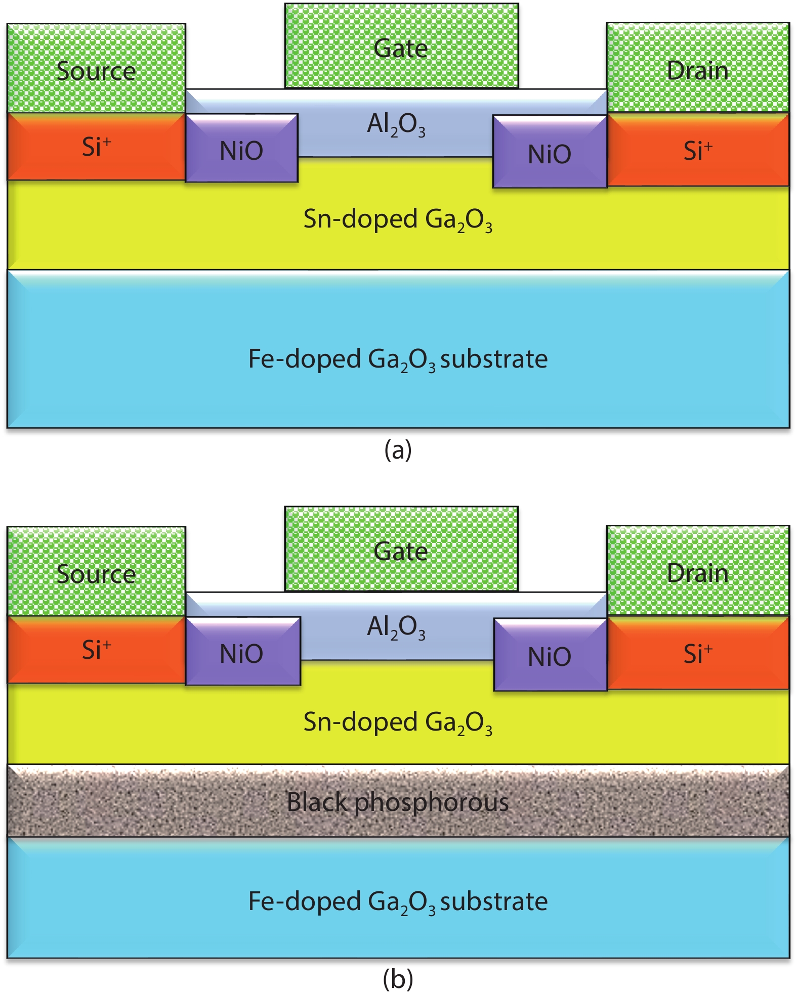
[22] N Yadava, R K Chauhan. RF performance enhancement of gallium oxide MOSFET using p-type NiO pocket near source and drain regions. J Telecomm, Electron Comput Eng, 11, 19(2019).
[23]
[24] K Zeng, J S Wallace, C Heimburger et al. Ga2O3 MOSFETs using spin-on-glass source/drain doping technology. IEEE Electron Device Lett, 38, 513(2017).
[25]
[26] K Sasaki, M Higashiwaki, A Kuramata et al. Si-ion implantation doping in