
Ja Hoon Koo, Huiwon Yun, Woongchan Lee, Sung-Hyuk Sunwoo, Hyung Joon Shim, Dae-Hyeong Kim. Recent advances in soft electronic materials for intrinsically stretchable optoelectronic systems[J]. Opto-Electronic Advances, 2022, 5(8): 210131
- Opto-Electronic Advances
- Vol. 5, Issue 8, 210131 (2022)
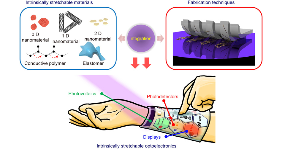
Fig. 1. Strategy for the development of intrinsically stretchable optoelectronics, based on intrinsically stretchable materials and novel fabrication techniques.
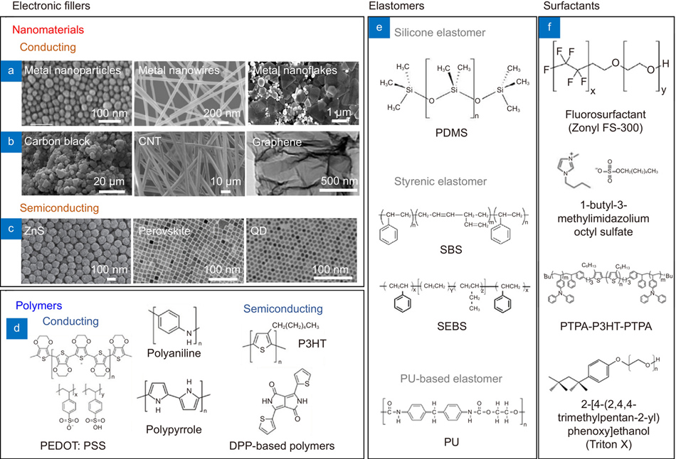
Fig. 2. Constituents of intrinsically stretchable conducting and semiconducting nanocomposites. Various (a –d ) electronic filler materials, (e ) elastomers, and (f ) surfactants are employed to develop intrinsically stretchable conducting/semiconducting nanocomposites. Figure reproduced with permission from: (a) ref.63, RSC Publishing, ref.64, IOP Publishing, ref.65, under a Creative Commons Attribution-Non Commercial 3.0 Unported License; (b ) ref.66, 67, under a Creative Commons Attribution 4.0 International License, ref.68, RSC Publishing; (c ) ref.80, 82, John Wiley and Sons, ref.81, under a Creative Commons Attribution 4.0 International License.
Fig. 3. Various conducting/semiconducting nanocomposites with intrinsic stretchability. Intrinsically stretchable conducting nanocomposites based on: (a ) CB and silica particles; (b ) SWCNTs and PU-PEDOT:PSS; (c , d ) Ag-Au NWs and SBS; and (e , f ) PEDOT:PSS incorporated with STEC enhancer. Intrinsically stretchable semiconducting nanocomposites based on: (g ) ZNS:Cu microparticles and PDMS; (h ) MAPbBr3 microparticles and PEO; (i –k ) P3HT nanofibers and SEBS; and (l ) DPPT-TT nanofibers and SEBS. Figure reproduced from: (a) ref.121, (b) ref.150, American Chemical Society; (c, d) ref.111, Springer Nature; (e, f) ref.125, under a Creative Commons Attribution-NonCommercial 4.0 International License; (g) ref.151, (i) ref.141, (j, k) ref.142, John Wiley and Sons; (l) ref.143, American Association for the Advancement of Science.
Fig. 4. Representative fabrication methods of intrinsically stretchable electronic materials. (a ) Schematic describing stencil printing method and (b ) optical image of the patterned Ag flake nanocomposite. Scale bar: 10 mm. (c ) Schematic of a soft lithography method for patterning intrinsically stretchable materials. (d ) Schematic showing inkjet printing of intrinsically stretchable materials. (e ) Schematic description of 3D printing process for intrinsically stretchable materials. (f ) Optical image of 3D-printed graphene/PDMS composite. (g ) Schematic for laser patterning of intrinsically stretchable materials. (h ) Optical image of the laser-patterned Ag NW/TPU nanocomposite, laminated on a textile with different line widths. Inset shows an SEM image of the Ag NW/TPU pattern. Scale bar: 5 mm. (i ) Digital image of a deformed textile patch. (j ) Schematics describing the photolithography process. (k ) Optical image of the Ag NW-based micropatterns on polyethylene glycol. Scale bar: 5 mm. (l ) An SEM image of the Ag NW micropatterns on a glass substrate. Figure reproduced with permission from: (b) ref.154, under a Creative Commons Attribution-NonCommercial-NoDerivs 4.0 International License; (f) ref.158, (h, i) ref.160, American Chemical Society; (k, l) ref.162, Creative Commons Attribution 4.0 International License.
Fig. 5. Optically active materials with intrinsic stretchability. (a ) PeNCs mixed in SEBS and its (b ) PL intensity and (c ) PL quantum yield with respect to various applied strains. (d ) Intrinsically stretchable emitting layer based on perovskite microcrystals in PEO. (e ) SEM images of the layer before and during stretching with different strains. (f ) PL intensity of the layer before and during stretching with 50% strain. (g ) Photo-absorbing blended film of PBDTTTPD:P(NDI2HD-T) with intrinsic stretchability. (h ) Stress-strain curve showing the elastic modulus and (i ) toughness measurement results of the blend film. (j ) Schematic of photo-absorbing layer fabrication based on mixture of PTB7-Th, IEICO-4F, and PDMS. (k ) Schematic showing the role of PDMS for intrinsic stretchability. (l ) The crack onset strain and elastic modulus of the film with respect to different PDMS concentrations. Figure reproduced with permission from: (a–c) ref.163, (d–f) ref.152, John Wiley and Sons; (g–i) ref.164, under a Creative Commons Attribution 4.0 International License; (j–l) ref.165, John Wiley and Sons.
Fig. 6. Charge transport materials with intrinsic stretchability. (a ) Intrinsically stretchable hole transport layer of Triton X-added PEDOT:PSS. (b ) Young’s modulus and crack onset strain (COS) of pristine and Triton X-added PEDOT:PSS layer. (c ) Raman spectroscopy analysis. (d ) SEM and (e ) AFM images of the film after applying strain of 160%. (f ) Intrinsically stretchable electron transport layer based on NBR and PFN. (g ) Optical microscope image showing clean film without any cracks developed after applying 60% strain. (h ) Current-voltage characteristics of the hybrid film. Figure reproduced with permission from: (a–e) ref.108, under a Creative Commons Attribution NonCommercial License 4.0. (f–h) ref.166, American Chemical Society.
Fig. 7. Intrinsically stretchable conductors in optoelectronic applications. (a ) AFM image of SWCNT-based elastomeric composite electrode. (b ) Optical transmittance of the electrode. Electrical performance of the electrode during (c ) different stretching strains and (d ) cyclic stretching test. (e ) Changes in surface morphology of intrinsically stretchable electrodes fabricated by mixing PEDOT:PSS, PEO, and Zonyl with different ratios. (f ) Change in resistance of the electrodes with respect to increasing the applied strain. (g ) Stability of the optimized electrode during cyclic stretching. Figure reproduced with permission from: (a–d) ref.168, (e–g) ref.170, John Wiley and Sons.
Fig. 8. LECs with intrinsic stretchability. (a ) Exploded view of hyperelastic LEC based on ZnS phosphor-doped stretchable EML and stretchable hydrogel electrodes. (b ) Stress-strain curves and (c ) relative illuminance measurements of the stretchable LEC. (d ) Photographs of the hyperelastic LEC during stretching. (e ) Multipixel display and (f ) bio-inspired skin display based on the hyperelasitc LEC. Figure reproduced with permission from: (a–f) ref.175, American Association for the Advancement of Science.
Fig. 9. LEDs with intrinsic stretchability. (a ) Structure of the intrinsically stretchable LED based on Go-soldered Ag NW/PUA composite electrodes and OXD-7 mixed white-light-emitting layer. (b ) Photographs of the stretchable LED before and during stretching. (c ) Stability of the stretchable LED after cyclic stretching tests. (d ) Chemical structure of a stretchable EML of PF-b-OU copolymer. (e ) Photograph of the stretchable LED during stretching with 150% strain. (f ) Change in luminance of the LED after stretching cycles. (g ) Structure of the stretchable LED based on small-molecule surfactant added stretchable layers. (h ) Luminescence and current density of the stretchable LED. Change in luminescence with respect to (j ) increasing strain and (j) stretching cycles. (k ) Photographs of the stretchable LED working after poking with a ballpoint pen. Figure reproduced from: (a–c) ref.176, American Chemical Society; (d–f) ref.177, John Wiley and Sons; (g–k) ref.109, under a Creative Commons Attribution NonCommercial License 4.0.
Fig. 10. PDs and PVs with intrinsic stretchability. (a ) Photograph of the intrinsically stretchable PD based on Zn2SnO4 NW/PDMS composite and Ag NW electrodes. (b ) Current-voltage characteristic of the PD. (c ) Photographs of the PD during stretching with different strains. (d ) Photoresponses of the PD with respect to applied strains with different amounts. (e ) Photograph of the intrinsically stretchable PD based on ZnO NW/PDMS composite and Ag NWs. (f ) Schematic showing the effect of stretching on the NW surface. Changes in (g ) on/off ratio and (h ) response time of the PD array at different stretching strains. (i ) Structure of intrinsically stretchable solar cell based on SWCNT/Ag NW-PUA composite electrodes and (PTB7)/PC71BM photo-absorbing layer. (j ) Photographs of the solar cell before and during stretching. Stability of the stretchable solar cell in terms of (k ) J-V characteristics and (l ) PCE during stretching. (m ) Structure of the intrinsically stretchable solar cell based on Ag NW/TPU composite electrodes and PTB7-Th:IEICO-4F heterojunction film. (n ) Schematic showing the adhesion of photo-absorbing layer and HTL. (o ) Optical image of the photo-absorbing layer under 20% strain. (p ) PCE of the solar cell during stretching. Figure reproduced with permission from: (a–d) ref.178, The Royal Society of Chemistry; (e–h) ref.179, John Wiley and Sons; (i–l) ref.180, American Chemical Society; (m–p) ref.165, John Wiley and Sons.
Fig. 11. Intrinsically stretchable optoelectronic systems. (a ) Photographs of an intrinsically stretchable alternating current EL display stably operating before and after stretching. (b ) Photographs of the intrinsically stretchable display mounted on hand skin. (c ) Photographs showing an intrinsically stretchable display being distorted by stretching. Figure reproduced with permission from: (a, b) ref.62, (c) ref.182, American Chemical Society.
| ||||||||||||||||||||||||||||||||||||||||||||||||||||||||||||||||||||||||||||||||||||||||||||||||||||||||||||||||||||||||||||||||||||||||||||||||||||||||||
Table 0. Electrical/mechanical performances of intrinsically stretchable conducting materials.
| |||||||||||||||||||||||||||||||||||||||||||||||||||||||||||||||||||||||||||||||||||||||||||||||||||||||||||||||||||||||||||||||||||
Table 0. Electrical/mechanical performances of intrinsically stretchable semiconducting materials.

Set citation alerts for the article
Please enter your email address
© Copyright 2018-2021 | Chinese Laser Press. All Rights Reserved 沪ICP备15018463号-20