Abstract
In recent years, significant progress has been achieved in the design and fabrication of stretchable optoelectronic devices. In general, stretchability has been achieved through geometrical modifications of device components, such as with serpentine interconnects or buckled substrates. However, the local stiffness of individual pixels and the limited pixel density of the array have impeded further advancements in stretchable optoelectronics. Therefore, intrinsically stretchable optoelectronics have been proposed as an alternative approach. Herein, we review the recent advances in soft electronic materials for application in intrinsically stretchable optoelectronic devices. First, we introduce various intrinsically stretchable electronic materials, comprised of electronic fillers, elastomers, and surfactants, and exemplify different intrinsically stretchable conducting and semiconducting composites. We also describe the processing methods used to fabricate the electrodes, interconnections, charge transport layers, and optically active layers used in intrinsically stretchable optoelectronic devices. Subsequently, we review representative examples of intrinsically stretchable optoelectronic devices, including light-emitting capacitors, light-emitting diodes, photodetectors, and photovoltaics. Finally, we briefly discuss intrinsically stretchable integrated optoelectronic systems.In recent years, significant progress has been achieved in the design and fabrication of stretchable optoelectronic devices. In general, stretchability has been achieved through geometrical modifications of device components, such as with serpentine interconnects or buckled substrates. However, the local stiffness of individual pixels and the limited pixel density of the array have impeded further advancements in stretchable optoelectronics. Therefore, intrinsically stretchable optoelectronics have been proposed as an alternative approach. Herein, we review the recent advances in soft electronic materials for application in intrinsically stretchable optoelectronic devices. First, we introduce various intrinsically stretchable electronic materials, comprised of electronic fillers, elastomers, and surfactants, and exemplify different intrinsically stretchable conducting and semiconducting composites. We also describe the processing methods used to fabricate the electrodes, interconnections, charge transport layers, and optically active layers used in intrinsically stretchable optoelectronic devices. Subsequently, we review representative examples of intrinsically stretchable optoelectronic devices, including light-emitting capacitors, light-emitting diodes, photodetectors, and photovoltaics. Finally, we briefly discuss intrinsically stretchable integrated optoelectronic systems.Introduction
Stretchable optoelectronic devices (e.g., light-emitting capacitors (LECs), light-emitting diodes (LEDs), photodetectors (PDs), and photovoltaics (PVs)) have been investigated significantly over the past decade and its utility has been demonstrated in several applications such as soft robotics1, 2, wearable optical sensors3-7, wearable smart displays8-10, and bio-integrated healthcare systems11-13. Intrinsically-stretchable features of the optoelectronic devices enable various novel device applications, especially human-friendly mobile and wearable electronics/optoelectronics applications. Therefore, both academia and industry have devoted substantial research efforts to develop and translate the futuristic device concepts into practical and user-friendly device applications. For instance, personal biometric information can be continuously monitored with high accuracy by using wearable and/or implantable optical sensing systems, such as an integrated device of LEDs and PDs, in a point-of-care manner. The measured physiological information can be used for real-time health monitoring and on-site diagnosis, which will be helpful for the early-diagnosis of many critical symptoms and the prevention of fatal health damages in the emergency situations. Such novel bio-integrated optoelectronic systems would provide new opportunities for remote and ubiquitous healthcare. However, there are several obstacles that prevent the large-scale fabrication of high-performance stretchable optoelectronic devices. Especially, further investigations are required on novel material components and their combinations for intrinsically stretchable device components to ensure that they have the desired optical, electrical, and mechanical properties (e.g., transparency, bandgap, and stretchability)14-18.
Ideally, stretchable optoelectronic devices should have a comparable performance to that of non-stretchable optoelectronic devices, especially in terms of key performance factors such as high areal coverage, high-quality light-emission, high-sensitivity photodetection, and high pixel resolution. In general, two different approaches have been pursued to achieve such stretchable optoelectronics – structure-based approaches and material-based approaches. Several studies have been conducted on stretchable optoelectronic devices that employ unconventional device designs (e.g., serpentine design19-21 and buckled structure22-24) and rigid semiconducting optoelectronic materials25-29. Notably, these devices have exhibited high optical and electrical performances, which are comparable to those of rigid devices, and high mechanical deformability. However, structural engineering-based device designs decrease the overall density of the device as additional space is required for structural interconnects, decreasing the array resolution. Moreover, rigid device components can cause a mechanical mismatch with the soft materials that interface with the device, such as with soft human tissues in the case of bio-integrated optoelectronics, leading to consequential side-effects such as skin irritations30-34.
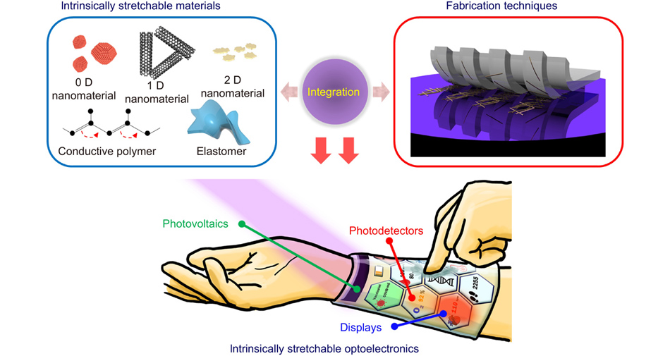
Owing to the limitations of structure-based approaches, material-based approaches have received significant attention in recent years. In general, existing research on material-based approaches have been focused on the synthesis of novel soft electronic materials and their application to device fabrication35-39. In particular, elastomeric composites, wherein various conducting/semiconducting electronic fillers (e.g., metal-based nanomaterials40-42, carbon-based nanomaterials43-45, and conjugated polymers46-48) are mixed inside elastomeric polymers, and their fabrication techniques have been studied extensively (Fig. 1 top). Intrinsically stretchable optoelectronic devices with soft electronic materials can endure mechanical deformations without the need for additional structural engineering. Consequently, soft-material-based optoelectronic devices are suitable for large-area fabrication with high pixel density, large areal coverage, and facile bio-integration with the human body (Fig. 1 bottom).

Figure 1.Strategy for the development of intrinsically stretchable optoelectronics, based on intrinsically stretchable materials and novel fabrication techniques.
This article reviews the recent advances in soft electronic materials for intrinsically stretchable optoelectronic devices. First, we introduce the constituents of intrinsically stretchable electronic materials, which can be classified into electronic fillers, elastomers, and surfactants. These materials are combined with each other to prepare intrinsically stretchable conducting and semiconducting composites. The processing methods of these soft electronic composites, which are used to fabricate various devices, are reviewed as well. Subsequently, we explore individual device components, such as stretchable electrodes, interconnections, charge transport layers, and optically active layers, and review representative examples of intrinsically stretchable optoelectronic devices, such as intrinsically stretchable LECs, LEDs, PDs, and PVs. Finally, we present examples of intrinsically stretchable integrated optoelectronic systems and conclude this review with a brief discussion on the remaining challenges of intrinsically stretchable optoelectronic devices.
Basic constituents of intrinsically stretchable electronic materials
Intrinsically stretchable electronic materials are required to fabricate intrinsically stretchable optoelectronic devices. All the device components, including the electrodes, interconnections, and charge transport layers/optically active layers, must be intrinsically stretchable, with controllable transparency and carrier dynamics. In terms of stretchable conductors, metallic nanomaterials such as nanowires and nanofibers have been widely investigated since their high aspect ratio grants substantial stretchability when assembled in network structures49, 50. Carbon-based nanostructures such as carbon nanotubes and graphene (flakes) have also been used as stretchable conductors, owing to their high aspect ratios and soft carbon-based material constructions51, 52. Other stretchable conductors include: metallic nanomesh53, wherein stretchability is achieved by morphological reconstruction of the photo-patterned thin metal film deposited on the elastomeric substrate, ionic conductors54, 55, which are composed of hydrogels with conductive ions or ionic liquids, and liquid metals56, 57 which consist of metal components with low toxicity such as Ga, Ga alloyed with In (EGain), and Ga alloyed with In and Sn (Galinstan).
In terms of stretchable optically-active layers, elastomeric composites consisting of optically-active polymers have been widely used. As such, functional elastomeric composites, wherein conducting or semiconducting electronic fillers and surfactants are incorporated in elastomeric matrices, have been extensively investigated for stretchable optoelectronic device applications58-62. The electrical, optical, and mechanical properties of these functional composites can be optimized for desired applications by controlling the mixing ratios of the individual material components. Since several excellent reviews on the stretchable conductors and fabrication of intrinsically stretchable elastomeric composites are already available40-48, we mainly focus on introducing various types of electronic filler materials, elastomers, and surfactants that can constitute electrically/optically functional elastomeric composites (Fig. 2).
Figure 2.Constituents of intrinsically stretchable conducting and semiconducting nanocomposites. Various (a–d) electronic filler materials, (e) elastomers, and (f) surfactants are employed to develop intrinsically stretchable conducting/semiconducting nanocomposites. Figure reproduced with permission from: (a) ref.63, RSC Publishing, ref.64, IOP Publishing, ref.65, under a Creative Commons Attribution-Non Commercial 3.0 Unported License; (b) ref.66, 67, under a Creative Commons Attribution 4.0 International License, ref.68, RSC Publishing; (c) ref.80, 82, John Wiley and Sons, ref.81, under a Creative Commons Attribution 4.0 International License.
Electronic filler materials
The optoelectronic properties of soft elastomeric composites such as their electrical conductivity, carrier mobility, and light emission/absorption ability, are primarily dependent on the incorporated electronic fillers. These electronic fillers, which are either conducting or semiconducting in nature, form percolation networks inside the elastomeric matrices that remain undamaged and interconnected under mechanical deformations, thereby maintaining their electronic and/or optoelectronic properties. In general, the optoelectronic performance of soft elastomeric composites can be improved by increasing the weight fraction of the electronic fillers in the composites. This increases the junction density in the percolation network and improves the electrical/optoelectrical performance of the composite. However, owing to the reduced elastomer fraction, the mechanical deformability of the composite decreases and its stiffness increases. Therefore, the type and concentration of the electronic fillers must be carefully considered to obtain the desired electronic/optoelectronic performance, while retaining the beneficial mechanical properties of the soft composites.
Nanomaterials and polymers are the most commonly used electronic fillers in soft conducting and/or semiconducting composites (Fig. 2(a))63-65. Metallic nanomaterials have been widely used as conducting electronic fillers in stretchable conductive composites owing to their high conductivity and flexibility in a networked structure. Gold, silver, and platinum nanostructures with zero-, one-, and two-dimensional (0D, 1D, and 2D, respectively) geometries are representative examples of metallic nanomaterials. Carbon-based nanomaterials have also been commonly used as conductive electronic fillers in soft composites (Fig. 2(b))66-68. Despite their relatively lower electrical conductivity compared to that of metallic nanomaterials, their low mass density enables the fabrication of highly durable and lightweight stretchable devices. Moreover, the electronic properties of 1D carbon nanostructures (i.e., single-walled carbon nanotubes, SWCNTs) can be controlled based on their chirality69, 70, thereby enabling the preparation of semiconducting electronic fillers and composites as well as stretchable conducting composites.
The geometrical dimensions of electronic fillers also have a significant effect on the electrical and mechanical performances of the resulting soft composites. For instance, 1D nanomaterials can form better percolation networks than multi-dimensional nanomaterials as a lesser amount of the nanomaterials is required to form an interconnected network owing to their high aspect ratio. This either increases the deformability of the resulting soft composites or increases the conductivity while providing the same mechanical performance as a comparable composite made of multi-dimensional nanomaterials. Owing to the lower weight fraction of the nanomaterial, the weight fraction of the elastomer in the composite increases, thereby enhancing the mechanical properties, such as stretchability and softness, of the composite.
Various semiconducting nanomaterials have been also employed as electronics fillers in soft composites, including ZnS nanoparticles (NPs)71-73, perovskite nanocrystals (PeNCs)74-76, and quantum dots (QDs)77-79, owing to their distinctive optoelectronic properties such as emission and/or absorption of light (Fig. 2(c))80-82. ZnS NPs can be used in applications that require light emissive electronic fillers in the soft composite, as their electroluminescence can be easily modulated by incorporating different types of dopants that form sulfide compounds. Metal halide PeNCs exhibit several desirable optoelectronic properties such as high exciton binding energies, photoluminescent quantum yields, and tunable bandgaps. In addition, their absorption/emission spectra can be easily tuned from the blue light range to the near-infrared light range by altering the chemical composition of the PeNCs. Therefore, they have a significant potential for application as optoelectronic semiconducting filler materials. Finally, core-shell type QDs are also considered to be good filler materials owing to their easily controllable and wide absorption/emission spectrum and high quantum yield83, 84.
In addition to the aforementioned nanomaterials, conjugated polymers85-87 can serve as conducting or semiconducting filler materials for fabricating intrinsically stretchable composites (Fig. 2(d)). Conjugated polymers not only exhibit facile miscibility with elastomers, but also have tunable charge transport properties, good transparency, and light weight. Furthermore, the band gap energies of conductive conjugated polymers can suitably align with the energy level of optically active layers (i.e., photo-absorption layers or light-emitting layers). Some representative examples of conductive conjugated polymer fillers include poly(3,4-ethylenedioxythiophene): polystyrene sulfonate (PEDOT:PSS)88, 89, polyaniline (PANI)90, 91, and polypyrrole92, 93. Semiconducting conjugated polymer fillers, such as poly(3-hexylthiophene) (P3HT)94, 95 and diketopyrrolopyrrole-based (DPP-based) polymers96, 97, have also been studied extensively.
Elastomers
The mechanical properties, such as the tensile strength, Young’s modulus, and stretchability, of the intrinsically stretchable materials are primarily dependent on the mechanical properties and weight fraction of the elastomeric matrices that envelop the percolation networks of the electronic fillers98-100. The mechanical characteristics of elastomers are determined by the degree of crosslinking of the polymer chains. Dense and strong crosslinking of the polymeric chains, which is made possible by the formation of side chains that connect long polymer chains, can result in relatively stiff but mechanically/chemically robust elastomers. In contrast, soft but fragile mechanical/chemical properties are induced when the crosslinking density is low.
In general, elastomers can be classified into chemically or physically crosslinked elastomers (Fig. 2(e)). In chemically crosslinked elastomers (e.g., silicone elastomers), the polymer chains are interconnected by covalent bonds, whereas in physically crosslinked elastomers (e.g., styrenic elastomers) the polymer chains are interconnected through relatively weaker ionic or hydrophobic interactions. Therefore, the mechanical freedom of physically crosslinked elastomers is generally higher than that of chemically crosslinked elastomers. Consequently, the processing and fabrication of physically crosslinked elastomers are much easier and more convenient in terms of solidification and reprocessing by heat, pressure, and solvents. Moreover, the maximum fraction of the electronic filler materials in chemically crosslinked elastomers is limited, as the crosslinking density can be decreased by an excessive amount of electronic fillers, resulting in poor controllability of the optoelectronic/mechanical properties. In contrast, physically crosslinked elastomers are relatively less affected by an excessive amount of additives. As a higher fraction of electronic fillers can be added to physically crosslinked elastomers, they have better electronic/optoelectronic performance, without any change in their mechanical performances.
Polyurethane (PU)-based elastomers are synthesized by reactions between di-/poly-isocyanates and macro-sized polyols, and exhibit both physical and chemical crosslinking. They have long soft blocks composed of polyol chains and hard blocks composed of urethane groups which involve the formation of hydrogen bonds. Furthermore, chemical crosslinking also occurs through allophanate bonding with other isocyanate groups. Therefore, PU-based elastomers exhibit the advantages of both types of crosslinking, i.e. facile processing, relatively high maximum loading of filler materials, and relatively high mechanical/chemical stability. They are frequently used in intrinsically stretchable optoelectronics owing to their excellent mechanical/chemical stability, facile processability, and high transparency101-103.
Besides being used as an elastic polymer matrix that envelops the electronic filler networks, elastomers are often used as an elastic substrate, electrical insulator, and/or encapsulation layer in intrinsically stretchable optoelectronic devices. Typical elastomers used for such purposes include chemically-crosslinked elastomers (e.g., silicone: polydimethylsiloxane (PDMS) and Ecoflex), physically-crosslinked elastomers (e.g., block-co-polymer: poly(styrene-butadiene-styrene) (SBS) and styrene-ethylene butylene-styrene (SEBS)), and elastomers that have both chemical covalent bonds and physical hydrogen bonds (e.g., polyurethane (PU)). These elastomers with the thickness of a micrometer range exhibit high optical transparency and reliable mechanical elasticity, both of which are critical factors for the use as substrates in intrinsically stretchable optoelectronic devices. Their low surface energies ensure smooth and uniform surfaces such that additional layers can be deposited on top using various deposition tools after proper surface treatments. Furthermore, these elastomers can potentially be used as a stretchable insulating layer in the phototransistor applications by reducing their thickness down to a few hundreds of nanometers. More detailed chemical and mechanical properties and their structural features can be found in other review articles97, 102.
Surfactants
The use of suitable surfactants (Fig. 2(f)) in the fabrication of intrinsically stretchable electronic materials can significantly improve the mechanical performance of the resulting composite materials104. Furthermore, compared to composites fabricated without any surfactant, the addition of a suitable surfactant can improve the electrical/optical performance of the composite by increasing the maximum loading amount of the functional fillers. Notably, the mechanical properties of the elastomeric composite are maintained by the surfactant, despite the higher fraction of the electronic fillers. Surfactants can also be used to modulate the surface energy of the material. For instance, a fluorosurfactant – Zonly FS – 300 was added to a PEDOT:PSS solution to improve its wetting, enabling the facile and uniform deposition of PEDOT:PSS films on various stretchable substrates105.
Surfactants can also be used to cause interchain reactions between the polymeric chains to modulate their electrical and mechanical performances. For example, the conductivity and stretchability of PEDOT:PSS films can be significantly enhanced by adding 1-butyl-3-methylimidazolium octyl sulfate – an ionic additives–assisted stretchability and electrical conductivity (STEC) enhancer106. The STEC enhancer induces an effective phase separation between the conductive PEDOT regions and the soft PSS regions and aggregates the PEDOT domain, thereby increasing the conductivity of the PEDOT:PSS film. The STEC enhancer also increases the stretchability of the PEDOT:PSS film owing to the softening of the PSS domains.
Meanwhile, a poly-(4-vinyltriphenylamine)-b-poly(3-hexylthiophene)-b-poly(4-vinyltriphenylamine) (PTPA-P3HT-PTPA) surfactant was used to suppress the aggregation of phenyl-C61-butyric acid methyl ester (PCBM) in a P3HT/PCBM composite mixture107. Specifically, the PTPA and PCBM domain mix inside the P3HT/PCBM composite, preventing the aggregation of PCBM. Solar cells based on these P3HT/PCBM films exhibited a higher power conversion efficiency than a control device.
A small-molecule surfactant such as 2-[4-(2,4,4-trimethylpentan-2-yl)phenoxy]ethanol (Triton X) can be also used to control the phase separation of polymeric chains. For instance, the addition of Triton X to a poly(phenylenevinylene) (PPV)-based intrinsically stretchable emissive material decreased interchain interactions, which increased the mechanical stretchability of the material108. Triton X has also been used to enhance the conductivity of PEDOT:PSS by inducing phase separation of the PEDOT and PSS domains109.
In Section Basic constituents of intrinsically stretchable electronic materials, various component materials (i.e., electronic fillers, elastomers, and surfactants) used for the development of functional elastomeric composites have been introduced. For the electronic fillers, either conducting or semiconducting fillers, their geometrical dimensions/shapes and the amounts/compositions to be added to the composite must be carefully considered for the optimized electrical, mechanical, and optical properties. Elastomers are used as either polymer matrices that carry the percolated networks of the electronic fillers to provide stretchability to the composite, or as substrates and insulation/encapsulation layers of the intrinsically stretchable devices. Surfactants are often adopted in the composites to enhance their electrical and mechanical properties, which can improve mechanical/electrical properties by inducing microscale phase separation and/or modulating the surface energy of the component materials.
Intrinsically stretchable electronic materials
In this section, we review actual examples of intrinsically stretchable conducting/semiconducting composites as well as their processing techniques, such as deposition and patterning methods. Representative examples of intrinsically stretchable conducting and semiconducting composites are listed in Tables 110, 110-132 and 287, 96, 133-149, respectively; they are categorized based on the type of filler or elastomer used in the composite, in addition to their electrical performance, mechanical properties, and applications. In the following, we focus on reviewing intrinsically stretchable conducting and semiconducting composites which were used in optoelectronic applications, such as stretchable transparent electrodes and stretchable photo-active layers.
Table Infomation Is Not EnableTable Infomation Is Not Enable
Intrinsically stretchable conducting and semiconducting composites
Figure 3(a–d) depict a few representatives of intrinsically stretchable conducting materials with 0D, 1D, and 2D nanomaterial-based electronic fillers. For example, Bhagavatheswaran et al. fabricated an intrinsically stretchable conducting composite using carbon black (CB) particles, spherical silica particles, and styrene butadiene rubber (SSBR) (Fig. 3(a))121. The CB and silica particles served as fillers, wherein the silica particles enhanced the percolation of the CB particles. Specifically, the silica particles applied high shear forces on the CB particles during the melt mixing process of the fillers in the SSBR, resulting in the dissociation and reduction in the size of the CB particles, which reinforced their percolation networks. The resulting intrinsically stretchable conducting composite had an electrical conductivity of 40 S/m, with a mechanical performance comparable to that of highly reinforced elastomer vulcanizate.
Figure 3.Various conducting/semiconducting nanocomposites with intrinsic stretchability.Intrinsically stretchable conducting nanocomposites based on: (a) CB and silica particles; (b) SWCNTs and PU-PEDOT:PSS; (c, d) Ag-Au NWs and SBS; and (e, f) PEDOT:PSS incorporated with STEC enhancer. Intrinsically stretchable semiconducting nanocomposites based on: (g) ZNS:Cu microparticles and PDMS; (h) MAPbBr3 microparticles and PEO; (i–k) P3HT nanofibers and SEBS; and (l) DPPT-TT nanofibers and SEBS. Figure reproduced from: (a) ref.121, (b) ref.150, American Chemical Society; (c, d) ref.111, Springer Nature; (e, f) ref.125, under a Creative Commons Attribution-NonCommercial 4.0 International License; (g) ref.151, (i) ref.141, (j, k) ref.142, John Wiley and Sons; (l) ref.143, American Association for the Advancement of Science.
Roh et. al. fabricated an optically transparent and stretchable conducting composite using SWCNTs and PU-PEDOT:PSS (Fig. 3(b))150. The intrinsic stretchability and optical transparency could be simultaneously achieved by the incorporation of SWCNTs with a low concentration. Despite the low concentration, the 1D nature of the SWCNTs facilitated effective percolation. Furthermore, the spin-coated SWCNTs on the PU-PEDOT:PSS layer maintained percolation with the PEDOT phases at the interfaces between the layers during stretching, thereby preserving the conductivity of the composite. The conductivity of the composite was further enhanced by stacking another PU-PEDOT:PSS layer on top, resulting in a sandwich-like stacked structure with higher mechanical stability.
Figure 3(c) and 3(d) illustrates the formation of an intrinsically stretchable conducting composite composed of 1D Au-coated Ag nanowires (Ag-Au NWs) in SBS111. The stretchability of the composite was further enhanced by inducing a phase separation to form separate conductive and stretchable regions. The phase separation forms a toluene-rich phase and a hexylamine-phase, which, after solvent evaporation, becomes a stretchable SBS-rich region and a conductive Ag-Au NW-rich region, respectively. The resulting optimized composite had a high conductivity of 41850 S/cm with a maximum stretchability of 840%.
An intrinsically stretchable conducting composite was also fabricated using 2D Ag flakes, fluorine rubbers, and fluorine surfactants117. Generally, pre-synthesized conducting nanomaterials are mixed with the elastomers while fabricating elastomeric conducting composites. However, in this case, Ag NPs were synthesized in situ during the mixing process, as Ag+ ions were diffused from the oxidized surfaces of the Ag flakes. The Ag NPs increased the electrical conductivity of the resulting elastomeric composite by condensing the percolated networks between the Ag flakes.
Figure 3(e) and 3(f) show examples of intrinsically stretchable conducting composites composed of conducting polymers126. Wang et al. fabricated a highly stretchable PEDOT:PSS film by adding STEC enhancers to PEDOT:PSS. The STEC enhancers modified the internal morphology of the film to promote stretchability and served as conductivity-enhancing dopants. Furthermore, owing to the addition of STEC enhancers, the rheological characteristics of the PEDOT:PSS film became similar to those of viscoelastic solids. In particular, the electrostatic interaction between the PEDOT and PSS domains was weakened by the introduction of the STEC enhancers, and PEDOT aggregate networks were formed inside the PSS matrices, resulting in a highly-conductive soft composite structure. Thus, an intrinsically stretchable film could be achieved, without mixing PEDOT:PSS with elastomeric materials.
Sustainable homogeneity of the elastomeric composite in an intrinsically stretchable semiconducting composite is essential for maintaining a uniform electrical performance, which is vital for optoelectronic device applications. Wang et al. fabricated an intrinsically stretchable semiconducting composite using ZnS:Cu microparticles and PDMS (Fig. 3(g))151. Owing to the chemically-stable nature of the PDMS, the homogeneously mixed ZnS:Cu microparticles could be well protected against solvent attack during the remaining device fabrication processes, resulting in robust emissive performances. Thus, simple fabrication of an electroluminescent (EL) device could be realized by directly embedding the electrodes into the polymer matrix. The ZnS:Cu/PDMS composite also exhibited excellent stretchability, as no significant degradation in its optoelectronic properties could be observed after being stretched up to 100%.
Bade et al. fabricated an intrinsically stretchable emissive composite by incorporating methylammonium lead tribromide (MAPbBr3) microparticles in a poly(ethylene oxide) (PEO) matrix (Fig. 3(h))152. Microscale MAPbBr3 particles were formed and embedded inside the PEO matrix through homogeneous mixing of the MAPbBr3 and PEO precursors in a weight ratio of 1:0.5. The composite solution was spin-coated and dried on a hot plate to obtain a pin-hole free film, wherein the gaps between the MAPbBr3 perovskite microcrystals were filled by the PEO polymer. Therefore, despite the mechanical fragility of the original perovskite material, the spin-coated film had excellent stretchable and optoelectronic properties, with the PEO matrix serving as an elastic connector.
In addition to 0D particles, 1D-structured nanofibers such as P3HT have also been widely used as semiconducting fillers in intrinsically stretchable composites. Shin et al. fabricated an intrinsically stretchable elastomeric composite by blending P3HT nanofibers with an SEBS elastomeric matrix, and then spin-coating the resulting mixture on a PDMS substrate (Fig. 3(i))141. The phase separation between the P3HT nanofibers and the SEBS matrix induced the formation of nanofiber bundles inside the blended mixture, providing good electrical performance. However, the stretchability of this composite was limited as the nanofiber bundles experienced severe cracking when an external strain was applied parallel to the aligned bundles. Song et al. solved this problem by directly embedding the P3HT nanofiber composites in the PDMS matrix (Fig. 3(j) and 3(k))142. The percolation networks of the P3HT nanofibers could rotate more freely under an applied strain as the PDMS matrix inhibited the formation of junctions between the nanofibers; however, tightly-bonded P3HT nanofibers without the PDMS matrix were broken under the applied strain.
The two studies discussed above developed intrinsically stretchable semiconducting composites using pre-grown nanofibers. Xu et al. devised a different method, wherein semiconducting polymer nanofibers of poly(2,5-bis(2-octyldodecyl)-3,6-di(thiophen-2-yl)diketopyrrolo[3,4-c]pyrrole-1,4-dione-altthieno[3,2-]thiophene) (DPPT-TT) developed percolation networks through the nanoconfinement effect during phase separation in SEBS (Fig. 3(l))143. The modulus of the conjugated polymer was reduced significantly owing to the increased polymer chain dynamics, thereby enhancing the stretchability of the composite without affecting its charge transport properties.
Fabrication methods for intrinsically stretchable composites
Functional elastomeric materials require proper processing before they can be fabricated into electronic components. They must be capable of being deposited as a uniform film and patterned into the desired design and/or structure. Conventional film deposition and photolithography-based patterning techniques involve vacuum-based deposition processes, photoresist development processes, and chemical/physical etching processes, which are rarely compatible with elastic materials. Therefore, several unconventional fabrication techniques have been introduced for depositing and patterning intrinsically stretchable electronic materials. This section will review some of the most widely used and state-of-the-art fabrication techniques that allow the processing of the intrinsically stretchable composites, such as printing and light-supported patterning techniques.
Various printing techniques that deposit an “ink” (i.e., intrinsically stretchable composites) onto a target substrate can be applied to the deposition and patterning of intrinsically stretchable materials. Stencil printing is one of the simplest printing processes, and only requires a patterning mask, a blade, and a solution-state material (Fig. 4(a))153. The mask is aligned on the substrate, and a uniform coating of the solution-phase target material is applied on the mask using the blade. The solidified material retains the desired pattern on the substrate after solvent evaporation (Fig. 4(b))154. However, although stencil printing is simple and cost-effective, the pattern edge may have a poor resolution owing to the surface tension of the solvent.
Figure 4.Representative fabrication methods of intrinsically stretchable electronic materials.(a) Schematic describing stencil printing method and (b) optical image of the patterned Ag flake nanocomposite. Scale bar: 10 mm. (c) Schematic of a soft lithography method for patterning intrinsically stretchable materials. (d) Schematic showing inkjet printing of intrinsically stretchable materials. (e) Schematic description of 3D printing process for intrinsically stretchable materials. (f) Optical image of 3D-printed graphene/PDMS composite. (g) Schematic for laser patterning of intrinsically stretchable materials. (h) Optical image of the laser-patterned Ag NW/TPU nanocomposite, laminated on a textile with different line widths. Inset shows an SEM image of the Ag NW/TPU pattern. Scale bar: 5 mm. (i) Digital image of a deformed textile patch. (j) Schematics describing the photolithography process. (k) Optical image of the Ag NW-based micropatterns on polyethylene glycol. Scale bar: 5 mm. (l) An SEM image of the Ag NW micropatterns on a glass substrate. Figure reproduced with permission from: (b) ref.154, under a Creative Commons Attribution-NonCommercial-NoDerivs 4.0 International License; (f) ref.158, (h, i) ref.160, American Chemical Society; (k, l) ref.162, Creative Commons Attribution 4.0 International License.
The stamping method has also been used to deposit intrinsically stretchable materials in a patterned manner (Fig. 4(c))155. In this method, the target materials are first spin-coated on a temporary substrate. Subsequently, a structured elastomeric stamp is applied on the target material with pressure and/or heat to pick up the material. Finally, the retrieved material is transfer-printed on the desired substrate. This technique can be employed for large-area patterning by repeating the aforementioned stamping process. The adhesion strength between the target material and the stamp or the receiving substrate must be carefully controlled to maximize the print yield and quality.
Solution-state functional elastomeric materials can also be deposited and patterned using inkjet printing. The “ink” is dropped on to the target substrate through a nozzle in the desired pattern (Fig. 4(d))156. The width and spacing of the pattern can be controlled by modulating the nozzle size, ink outlet power, nozzle speed, and ink viscosity. Compared to other methods such as screen printing or transfer printing, the inkjet printing method minimizes material wastage.
Owing to the recent advances in 3D printing processes, they can also be applied to the deposition and patterning of intrinsically stretchable materials (Fig. 4(e))157. In 3D printing, the first layer of a solution-state material is printed on a substrate. After the first layer solidifies, a second layer can be printed on top of the first layer. This process can be repeated to fabricate a 3D structure (Fig. 4(f))158. The target material must solidify quickly, and the orthogonality of the solvent between the adjacent layers must be considered. Firm and facile interlayer bonding is also vital to build a reliable 3D structure.
Light-supported patterning methods can also be used to pattern and fabricate intrinsically stretchable materials. The laser-cutting technique can pattern the target material using a high-energy laser ablation process (Fig. 4(g))159. The target material can be rapidly sliced, engraved, or marked with a high resolution (Fig. 4(h) and 4(i))160. However, flammable or heat-resistant materials cannot be used with this patterning method. In addition, some materials exhibit swelling under the high temperature.
Photolithography is a representative patterning process that transfers an original pattern of a photomask on to a target material. Notably, photolithography provides a remarkably high resolution. However, a photoresist should be coated on the target surface before ultraviolet exposure, which is then followed by chemical and/or physical etching processes (Fig. 4(j))161. These procedures often cannot be applied to intrinsically stretchable materials that contain elastic matrices. Therefore, methods have been developed wherein the filler materials are first patterned using photolithography and then embedded in the elastomeric matrix (Fig. 4(k) and 4(l))162. Therefore, elastomeric composites with various desired patterns of the functional fillers can be fabricated using this method.
In Section Intrinsically stretchable electronic materials, various examples of the intrinsically stretchable functional composites have been reviewed, with a focus on the materials. These composites incorporate the conducting and semiconducting fillers with diverse geometrical dimensions/shapes and employ various strategies for enhancing the dispersion/distribution of the filler materials in the elastomer matrix, which lead to the improvement of the mechanical, electrical, and optical properties of the composites. In addition, the recently developed techniques for the facile processing of the intrinsically stretchable functional composites have been briefly discussed. The application of these intrinsically stretchable functional composites as key material components of the intrinsically stretchable optoelectronic devices will be reviewed in the following section.
Components of intrinsically stretchable optoelectronic devices
The fabrication of intrinsically stretchable optoelectronic devices is typically involved with bottom-up material preparation processes, wherein intrinsically stretchable materials are prepared and used as components of the optoelectronic devices. Although various components are employed for different types of optoelectronic devices, they can be classified into three main categories based on their purposes: 1) active layers, either photo-emissive or photo-absorptive, which are used to achieve the desired optoelectronic properties; 2) charge-transport layers, which provide efficient charge transfer between the electrodes and the active layers; and 3) electrically conductive layers, which are used as electrodes and interconnects. In this section, we review various intrinsically stretchable device components for intrinsically stretchable optoelectronic devices based on this classification.
Intrinsically stretchable active layers
Intrinsically stretchable active layers either emit light through electroluminescence or absorb photon energy to detect external light despite severe mechanical deformation. They are usually composed of an elastic matrix and emissive/photo-absorbing nanomaterials. The elastic matrix prevents crack generation and propagation due to mechanical deformation. The materials and internal structure of the elastic matrix have a significant effect on the mechanical stability of the composite. The emissive/photo-absorbing nanomaterials primarily determine the emissive/photo-absorption spectrum and band-gap energy of the composite. Therefore, the mechanical and optoelectrical properties of the intrinsically stretchable active layers depend significantly on the types and internal/intramolecular structures of the elastic matrix and emissive/photo-absorbing nanomaterials.
In an intrinsically stretchable light-emissive layer, the injected electrons and holes are recombined to emit light through electroluminescence, even under mechanical deformations. Zhou et al. developed an intrinsically stretchable light emitting layer by mixing PeNCs encapsulated by ionic ligands with SEBS (Fig. 5(a))163. A freestanding stretchable light-emitting composite was prepared by spin-coating this on an octadecyltrimethoxysiliane (OTMS)-treated Si substrate, followed by evaporation of the solvent and peeling off of the film. The resulting PeNC/SEBS film exhibited good tolerance to mechanical deformations and external humidity. The photoluminescence (PL) intensity of the PeNC/SEBS film decreased slightly as the film stretched from zero to 100% (Fig. 5(b)). Nevertheless, when the mechanical strain on the PeNC/SEBS film was released, the PL intensity of the film almost recovered to its initial level. Furthermore, the PeNC/SEBS film maintained its high PL quantum yield (> 60%) and emissive spectrum even at a relative humidity of > 70% (Fig. 5(c)).
Figure 5.Optically active materials with intrinsic stretchability.(a) PeNCs mixed in SEBS and its (b) PL intensity and (c) PL quantum yield with respect to various applied strains. (d) Intrinsically stretchable emitting layer based on perovskite microcrystals in PEO. (e) SEM images of the layer before and during stretching with different strains. (f) PL intensity of the layer before and during stretching with 50% strain. (g) Photo-absorbing blended film of PBDTTTPD:P(NDI2HD-T) with intrinsic stretchability. (h) Stress-strain curve showing the elastic modulus and (i) toughness measurement results of the blend film. (j) Schematic of photo-absorbing layer fabrication based on mixture of PTB7-Th, IEICO-4F, and PDMS. (k) Schematic showing the role of PDMS for intrinsic stretchability. (l) The crack onset strain and elastic modulus of the film with respect to different PDMS concentrations. Figure reproduced with permission from: (a–c) ref.163, (d–f) ref.152, John Wiley and Sons; (g–i) ref.164, under a Creative Commons Attribution 4.0 International License; (j–l) ref.165, John Wiley and Sons.
Bade et al. fabricated an intrinsically stretchable emitting layer using a perovskite-polymer composite (Fig. 5(d))152. A perovskite precursor solution was mixed with PEO and spin-coated on a substrate. As the spin-coated film was heated, the perovskite precursor solution crystallized, forming micro-sized perovskite crystals inside the PEO matrix (left frame of Fig. 5(e)). The PEO matrix in the composite dissipates external mechanical strain, and the perovskite-polymer composite film can withstand an external strain of up to 30%, without any crack initiation (middle frame of Fig. 5(e)). The PEO matrix begins to crack under an external strain of 50% (right frame of Fig. 5(e)), resulting in a slight decrease in the PL intensity of the perovskite-polymer composite (Fig. 5(f)).
Photo-absorbing layers can absorb photon energy and form electron-hole pairs to generate electrical energy. Intrinsically stretchable photo-absorbing layers are generally fabricated using a non-fullerene acceptor and a plasticizer, which increases the mechanical stability of the composite. Kim et al. developed a highly-durable photo-absorbing layer by using a non-fullerene acceptor164. Specifically, a mixture of poly[4,8-bis(5-(2-ethylhexyl)thiophen-2-yl)benzo[1,2-b:4,5-b0]dithiophene-alt-1,3-bis(thiophen-2-yl)-5-(2-hexyldecyl)-4H-thieno[3,4-c]pyrrole-4,6(5H)-dione] (PBDTTTPD) and poly[[N,N0-bis(2-hexyldecyl)-naphthalene-1,4,5,8-bis(dicarboximide)-2,6-diyl]-alt-5,50-thiophene] (P(NDI2HD-T)), which acted as the electron donor and electron acceptor, respectively, were used in the photo-absorbing layer. Unlike fullerene-based acceptors, a non-fullerene acceptor like naphthalene diimide-based copolymer P(NDI2HD-T) exhibits an extended π-conjugated internal structure and intramolecular π-π stacking interactions, providing strong mechanical stability to the photo-absorbing layers. Owing to the internal/intramolecular structures of P(NDI2HD-T), no cracks were formed in the PBDTTTPD:P(NDI2HD-T) blended film even under a mechanical elongation of 6.3% (Fig. 5(g)). Compared to PBDTTTPD films with a fullerene-based acceptor, the PBDTTTPD:P(NDI2HD-T) blended film had a relatively low elastic modulus of 0.43 GPa and a high elongation of up to 7.16% (Fig. 5(h)). Furthermore, the toughness of the PBDTTTPD:P(NDI2HD-T) blended film was also significantly higher than that of PBDTTTPD films with fullerene-based acceptors (Fig. 5(i)).
Wang et al. fabricated a photo-absorbing layer by incorporating a trimethylsiloxy terminated PDMS additive into a mixture of a polymer donor and a non-fullerene acceptor165. The polymer donor was poly{4,8-bis[5-(2-ethylhexyl)thiophen-2-yl]benzo[1,2-b:4,5-b′]-dithiophene-2,6-diyl-alt-3-fluoro-2-[(2-ethylhexyl) carbonyl]-thieno[3,4-b]thiophene-4,6-diyl} (PTB7-Th), the non-fullerene acceptor was 2,2′-((2Z,2′Z)-(((4,4,9,9-tetrakis(4-hexylphenyl)-4,9-dihydro-sindaceno[1,2-b:5,6-b′]dithiophene-2,7-diyl)bis(4-((2-ethylhexyl)oxy)thiophene-5,2-diyl))bis (methanylylidene)) bis (5,6-difluoro-3-oxo-2,3-dihydro-1H-indene-2,1-diylidene))dimalononitrile (IEICO-4F), and the PDMS additive acted as the plasticizer. The three compounds were mixed together and spin-coated on top of an OTMS-treated glass substrate, and the film was peeled off (Fig. 5(j)). Without the PDMS, the PTB7-Th in the blended film exhibits strong interchain interaction between each polymer chain, resulting in a small free volume in the blended film (Fig. 5(k)). The incorporation of PDMS increases the free volume between the polymer chains owing to the plasticization of the film. The blended film with a small amount of PDMS had an elastic modulus of 0.99 GPa, and crack generation was hindered under a mechanical strain of up to 20% (Fig. 5(l)).
Intrinsically stretchable charge-transport layers
Charge transport layers are placed between the electrodes and the active layer of an optoelectronic device. They enable charge transport by aligning the band structures. Generally, intrinsically stretchable charge transport layers are fabricated by incorporating additives to alter the molecular interactions of the polymeric charge transport layers. Kim et al. fabricated intrinsically stretchable hole transport layers by incorporating a non-ionic surfactant into PEDOT:PSS and inducing strong phase separation (Fig. 6(a))109. Pristine PEDOT:PSS exhibits strong electrostatic interaction between the PEDOT chains, which form coil-like structures, resulting in a relatively high Young’s modulus (approximately 100 MPa) and a low crack onset strain (< 10%) (Fig. 6(b)). The addition of Triton X – a non-ionic surfactant – screens the electrostatic interaction of PEDOT:PSS and induces a strong phase separation. Consequently, the structure of the PEDOT chains in PEDOT:PSS changes from a coil-like structure to a linear structure, as confirmed by Raman spectroscopy (Fig. 6(c)). Owing to this linear structure, the Triton X containing PEDOT:PSS has a Young’s modulus of 2.5 MPa and a crack onset strain of over 160% (Fig. 6(b), 6(d), and 6(e)). Thus, it can withstand severe mechanical deformation and serve as an intrinsically stretchable charge transport layer.
Figure 6.Charge transport materials with intrinsic stretchability. (a) Intrinsically stretchable hole transport layer of Triton X-added PEDOT:PSS. (b) Young’s modulus and crack onset strain (COS) of pristine and Triton X-added PEDOT:PSS layer. (c) Raman spectroscopy analysis. (d) SEM and (e) AFM images of the film after applying strain of 160%. (f) Intrinsically stretchable electron transport layer based on NBR and PFN. (g) Optical microscope image showing clean film without any cracks developed after applying 60% strain. (h) Current-voltage characteristics of the hybrid film. Figure reproduced with permission from: (a–e) ref.108, under a Creative Commons Attribution NonCommercial License 4.0. (f–h) ref.166, American Chemical Society.
Hsieh et al. developed an intrinsically stretchable electron transport layer by mixing nitrile butadiene rubber (NBR) with poly[(9,9-bis(3′-(N,N-dimethylamino)propyl)-2,7-fluorene)-alt-2,7-(9,9-dioctylfluorene)] (PFN)166. When NBR is mixed with PFN, the carboxyl group in NBR protonates and chemically interacts with the amine groups in PFN (Fig. 6(f)). The interactions between NBR and PFN significantly increase the ductility of the hybrid NBR/PFN film. Consequently, it can withstand mechanical deformation under an external strain of up to 60% (Fig. 6(g)). Furthermore, the protonation of PFN increases its solubility in a polar solvent and modifies its work function, thereby improving the charge transport properties of the hybrid NBR/PFN film (Fig. 6(h)).
In a recent report by Matsuhisa et al, detailed strategies for developing the stretchable anode, cathode, and current collecting layer have been reported, of which the mechanical property, work function, and processability of the stretchable films could be deliberately controlled for the fabrication of the intrinsically stretchable device with desired electrical and mechanical properties167. For the stretchable anode, a blend film of PEDOT:PSS, fluorosurfactant (FS30), and a zwitterion 4-(3-ethyl-1-imidazolio)−1-butanesulfonate (ION E) was developed. FS30 was incorporated to facilitate surface wetting of the solution, and ION E served as both a stretchability enhancer and a work function changer. The blend film exhibited the crack-on-set strain at 93% and a work function of 5.23 eV, which was controlled to form ohmic contact with the semiconductor, 3,6-di(thiophen-2-yl)diketopyrrolo[3,4-c]pyrrole-1,4-dione-alt-1,2-dithienylethene (DPP4T-oSi10). For the stretchable cathode, a blend film of PEDOT:PSS, ION E, and a high-molecular-weight PSSNa (molar weight = 1 MDa) was developed. The PSSNa was incorporated to tune the viscosity of the blended solution for stencil printing. The surface of the deposited stretchable film was modified using polyethylenimine ethoxylated (PEIE), which lowered the work function to 4.73 eV to form Schottky contact with DPP4T-oSi10. Finally, a stretchable composite using Ag NWs and tough thermoplastic PU (TPU) was developed for the stretchable current collector. The importance of the mechanical property of the elastomeric matrix was verified by embedding Ag NWs in various elastomers such as soft SEBS, tough SEBS, soft TPU, and tough TPU. The stretching test results revealed that only the tough TPU-based composite exhibited no crack formation at 50% strain, which was critical to the device performance.
Intrinsically stretchable electrodes and interconnects
The intrinsically stretchable optoelectronic devices emit light under an applied electrical bias (e.g., light emitting diode), transform light energy into electrical energy (e.g., photovoltaic device), or respond to light sources of various wavelengths with photocurrent generation (e.g., photodetector). It is important that light can be effectively emitted or garnered from the photoactive layers that are interfaced with the electrodes, and thus such electrodes need to simultaneously exhibit key properties including high optical transparency, high mechanical stability, and high conductivity. In general, these properties can be manipulated by controlling the amount of the electronic fillers added to the elastomeric matrices. The general material guideline and consequent electrode properties are as follows. Higher amounts of the fillers result in the improved electrical performance, however, in sacrifice of the optical transmittance and stretchability. Lower amounts of the fillers result in the improved transparency of the composite, but the electrical performance as well as the mechanical performance might be sacrificed owing to the easy disconnection of the percolation networks of the low-density fillers. Therefore, in the following, several strategies for optimizing the intrinsically stretchable electrodes and interconnects will be reviewed, in terms of materials used and fabrication methods.
Yu et al. developed transparent SWCNT-based elastomeric composite electrodes, which were applied to poly(tert-butyl acrylate) (PtBA)-based LECs168. The SWCNT-polymer composite electrodes were prepared through photopolymerization of a liquid-state monomer during its penetration into a porous SWCNT film on a glass substrate, and were then peeled off from the substrate. As shown in the atomic force microscopy image in Fig. 7(a), the SWCNT networks were well-percolated in the elastomeric matrix of PtBA, with exceptional surface smoothness (average surface roughness below 10 nm). Owing to their high optical transmittance (Fig. 7(b)) and stable electrical conductance (Fig. 7(c) and 7(d)) up to a strain of 50%, these electrodes were applied as both the anode and the cathode in a stretchable polymer-based LEC, which comprised of a polymeric emissive layer sandwiched between the stretchable electrodes. The EL properties of the fabricated device remained unchanged up to a strain of 45%.
Figure 7.Intrinsically stretchable conductors in optoelectronic applications. (a) AFM image of SWCNT-based elastomeric composite electrode. (b) Optical transmittance of the electrode. Electrical performance of the electrode during (c) different stretching strains and (d) cyclic stretching test. (e) Changes in surface morphology of intrinsically stretchable electrodes fabricated by mixing PEDOT:PSS, PEO, and Zonyl with different ratios. (f) Change in resistance of the electrodes with respect to increasing the applied strain. (g) Stability of the optimized electrode during cyclic stretching. Figure reproduced with permission from: (a–d) ref.168, (e–g) ref.170, John Wiley and Sons.
Wang et al. fabricated stretchable and transparent electrodes using welded networks of Cu NWs embedded on the surface of pre-strained Ecoflex169. The electrodes were used in stretchable organic solar cells and commercial LEDs. The fabrication process was as follows. First, thin films of Cu NW networks were prepared through vacuum filtration. The resulting films were treated with hydrogen plasma for 20 min to remove the organic residues and surface oxides, while simultaneously welding the Cu NWs. This welding method can help achieve high stretchability and conductivity, by preventing the sliding of the NWs during repetitive deformations. As such, no debonding or breakage of the Cu NWs occurred during stretching. These durable Cu NW-based electrodes can replace indium tin oxide (ITO) as the transparent electrode in solar cells, and can be used as interconnects in commercial LEDs under various deformation modes.
Dauzon et al. systematically investigated the electrical and mechanical performances of the intrinsically stretchable electrodes that were fabricated by mixing PEDOT:PSS, PEO, and Zonyl170. The 3D matrix of PEO provides high mechanical recoverability and elasticity, and the incorporation of Zonyl improves the ductility of PEDOT:PSS. They revealed that the inclusion of 5 wt% of PEO and 1 wt% of Zonyl optimized the electrode performance: no crack formation occurred till an applied strain of 80% (Fig. 7(e)), minimized resistance changes occurred at an applied strain of 80% (Fig. 7(f)), and the electrodes exhibited high stability under a cyclic stretching up to a strain of 80% (Fig. 7(g)). The fabricated stretchable electrodes also exhibited a high optical transmittance of approximately 95% at 550 nm. The practical feasibility of these stretchable electrodes was verified by fabricating solar cells, which had a power conversion efficiency of 12.5%.
Ionic conductors (or so called electrolytes), which use ions as current carriers, have also been mixed with elastomers to simultaneously achieve high transparency, conductivity, and elasticity. Shi et al reported on the facile fabrication of an ionic conducting elastomer (ICE) by using an instant photocuring process. Specifically, lithium bis(trifluoromethane sulfonimide) (LiTFSI), butyl acrylate (BA), polyethyleneglycol diacrylate (PEGDA), 1-hydroxycyclohexyl phenyl ketone (photo-initiator 184) were used as the electrolyte salt, monomer, crosslinker, and photo-initiator, respectively. Due to its solvent-free nature, the ICE, which was produced by curing the mixture solution injected onto a glass mold coated with a release film with ultraviolet light for 10 minutes, exhibited excellent air stability. The ICE was also not corrosive to common metal electrodes since it does not contain any water nor absorb any moisture from the air. A 1-mm thick sample displayed a transmittance of 92.4% at 550 nm, a conductivity of 1.27 × 10⁻⁷ S/cm, and stretchability with an elongation at break of approximately 1100%. Moreover, the decomposition voltage of the developed ICE was several times higher than that of the hydrogel electrolytes, making the ICE an appealing material candidate for the stretchable and transparent electrode.
The intrinsically stretchable functional composites have been applied as stretchable active layers, charge transport layers, and electrodes to construct the intrinsically stretchable optoelectronic devices. Whereas each device component of the intrinsically stretchable optoelectronic devices has been reviewed in Section 4 in terms of the performance metrics and fabrication methods, the details of the various intrinsically stretchable optoelectronic devices (Section Intrinsically stretchable optoelectronic devices) and optoelectronic systems (Section Intrinsically stretchable optoelectronic systems) will be reviewed in the following sections.
Intrinsically stretchable optoelectronic devices
As discussed in Section Components of intrinsically stretchable optoelectronic devices, the bottom-up approach is generally adopted to fabricate intrinsically stretchable optoelectronic devices, wherein the constituent materials are first prepared separately and then assembled together to construct the target devices. Consequently, compatibility between the constituent materials is important, especially in terms of their processing and materials properties. The detailed working mechanisms of various optoelectronic devices can be readily found elsewhere171-173. In this section, we review various intrinsically stretchable optoelectronic devices, such as LECs, LEDs, PDs, and PVs, with a focus on their constituent materials and processing methods.
Intrinsically stretchable LECs
Intrinsically stretchable light-emitting devices have several next-generation applications such as foldable/expandable displays, epidermal biomedical devices, and deformable mobile electronic devices. As the constituent elements of the devices must be intrinsically stretchable, LECs, which have simpler structures compared to LEDs, have been investigated for application to stretchable light-emitting devices. The key challenge has been to sustain the light-emitting performances such as emission intensity under large strains and maintain their functionalities after large strain cycles. Thus, research efforts have been focused on developing stretchable conductors and EL layers with high mechanical stability, and their integration strategies for enhanced durability.
Liang et al. fabricated elastomeric polymer light-emitting devices using transparent and stretchable Ag NW-poly(urethane acrylate) (PUA) composite electrodes and a polymer light-emitting electrochemical cell174. The polymer light-emitting electrochemical cell comprises of a blend of a yellow light-emitting polymer, PEO, ethoxylated trimethylolpropanetriacrylate, and lithium trifuoromethane sulphonate. The device had a simple structure with the polymer light-emitting electrochemical cell layer sandwiched between the composite electrodes to form an in situ light-emitting PIN junction, thereby enabling efficient hole and electron injection from the Ag NWs. By optimizing the ratio of siliconized urethane acrylate oligomer (UA) and ethoxylated bisphenol A dimethacrylate (EBA), they obtained stretchable composite electrodes with excellent optical transmittance and stretchability, providing stable performance under a strain of up to 120%. The scalability of the materials and the fabrication technique were demonstrated by developing a passive matrix display with a 5 × 5 pixel array, which exhibited stable operation under stretching.
Larson et al. fabricated LEC with an unprecedented stretchability of approximately 500%175. This hyperelastic LEC consisted of a ZnS phosphor-doped Ecoflex-based stretchable EL dielectric layer that was sandwiched between stretchable hydrogel electrodes (Fig. 8(a)). The electrodes were fabricated by dissolving N,N’’-methylenebisacrylamide crosslinker, polyacrylamide (PAM), and acrylamide monomer in aqueous LiCl, followed by sequential casting on an Ecoflex substrate and curing using ultraviolet irradiation. The electrodes exhibited high stretchability and transparency. Consequently, the LEC exhibited intrinsic stretchability, as confirmed by the stress-stretch curves (Fig. 8(b)) and relative illuminance measurements under uniaxial stretching (Fig. 8(c)). After encapsulating the device in Ecoflex, the fabricated LEC was stretched by nearly 500% without device failures (Fig. 8(d)). The practical feasibility of the stretchable LEC display was successfully demonstrated by developing multipixel displays (Fig. 8(e)) and a bio-inspired skin display (Fig. 8(f)).
Figure 8.LECs with intrinsic stretchability. (a) Exploded view of hyperelastic LEC based on ZnS phosphor-doped stretchable EML and stretchable hydrogel electrodes. (b) Stress-strain curves and (c) relative illuminance measurements of the stretchable LEC. (d) Photographs of the hyperelastic LEC during stretching. (e) Multipixel display and (f) bio-inspired skin display based on the hyperelasitc LEC. Figure reproduced with permission from: (a–f) ref.175, American Association for the Advancement of Science.
Intrinsically stretchable LEDs
Whereas LECs have a rather simple structure of a light-emitting dielectric layer sandwiched between two electrodes, LEDs require additional charge transport layers such as hole and electron injection layers. Consequently, the fabrication of intrinsically stretchable LEDs is more complex, requiring the development of intrinsically stretchable charge transport layers and their integration with the remaining layers. As discussed in Section Intrinsically stretchable charge-transport layers, few research efforts have been devoted toward the development of stretchable charge transport layers, and research on intrinsically stretchable charge transport layers and their integration in stretchable devices is still in its infancy. Nevertheless, several attempts have been made to develop intrinsically stretchable LEDs due to the advantages of LEDs such as low operation voltages, high luminance, and compatibility with the existing display industry. These approaches are reviewed in this section, with a focus on the materials used and their mechanical/optoelectronic performances.
Liang et al. fabricated fully stretchable polymer light-emitting diodes (PLEDs)176. They comprised of stretchable transparent conductive electrodes (TCEs) with graphene oxide (GO)-soldered Ag NW networks in PUA as both the cathode and the anode, polyethylenimine (PEI) as the electron transporting layer (ETL), PEDOT:PSS as the hole transporting layer (HTL), and 1,3-bis[(4-tert-butylphenyl)-1,3,4-oxidiazolyl]phenylene (OXD-7) mixed with a white-light-emitting polymer as the emission layer (EML) (Fig. 9(a)). The thicknesses of the HTL, ETL, and EML were optimized for the best mechanical and optoelectronic performances, resulting in a stretchability of 130% (Fig. 9(b)) and an endurance of up to 100 stretching cycles under a linear strain of 40% (Fig. 9(c)). Recently, Jao et al. fabricated stretchable blue LEDs using a poly[2,7-(9,9-dioctylfluorene)]-block-poly(isoprene) (PF-b-PI) copolymer as the stretchable EML. The effect of the PF/PI mixing ratios on the photoluminescent and mechanical properties of the stretchable LEDs was systematically investigated (Fig. 9(d))177. Using solution-based processes, stretchable LEDs were fabricated on a PU substrate (PEDOT:PSS/PEO and Ein-Ga were used as the anode and cathode, respectively), exhibiting a stretchability of 150% (Fig. 9(e)). The results of cyclic stretching tests revealed that the LEDs could stably maintain their optoelectronic performance under a linear strain of 20% (Fig. 9(f)).
Figure 9.LEDs with intrinsic stretchability.(a) Structure of the intrinsically stretchable LED based on Go-soldered Ag NW/PUA composite electrodes and OXD-7 mixed white-light-emitting layer. (b) Photographs of the stretchable LED before and during stretching. (c) Stability of the stretchable LED after cyclic stretching tests. (d) Chemical structure of a stretchable EML of PF-b-OU copolymer. (e) Photograph of the stretchable LED during stretching with 150% strain. (f) Change in luminance of the LED after stretching cycles. (g) Structure of the stretchable LED based on small-molecule surfactant added stretchable layers. (h) Luminescence and current density of the stretchable LED. Change in luminescence with respect to (j) increasing strain and (j) stretching cycles. (k) Photographs of the stretchable LED working after poking with a ballpoint pen. Figure reproduced from: (a–c) ref.176, American Chemical Society; (d–f) ref.177, John Wiley and Sons; (g–k) ref.109, under a Creative Commons Attribution NonCommercial License 4.0.
Kim et al. fabricated intrinsically stretchable organic light-emitting diodes (OLEDs), wherein all the constituent materials were modified with small-molecule surfactants to impart stretchability (Fig. 9(g))109. For the EML, a commercial emissive material Super Yellow (SY) was mixed with Triton X, which increased the stretchability of SY by reducing the number of interchain interactions. For the HTL, PEDOT:PSS was mixed with Triton X, and the resulting phase separation into PEDOT-rich and PSS-rich domains improved stretchability. For the ETL, doped polyethyleneimine ethoxylated (d-PEIE) and ZnO NPs were used; d-PEIE significantly lowered the work function and imparted stretchability to the composite. Finally, Ag NW networks were used as the anodes and cathodes; Ag NWs embedded in the PDMS matrix served as the anode, and Ag NWs that were directly coated on the stretchable ETL served as the cathode. The resulting stretchable OLED had a turn-on voltage of 8.3 V with a maximum luminescence of 2500 cd/m, which remains the highest reported value for an intrinsically stretchable light-emitting devices (Fig. 9(h)). Furthermore, the OLED maintained its excellent optoelectronic properties up to an applied strain of 40% (Fig. 9(i)), enduring 200 stretching cycles without any degradation in its luminescent properties (Fig. 9(j)). Notably, its stability remained unaffected even after it was poked with a ballpoint pen with a tip radius of 0.7 mm (Fig. 9(k)). Therefore, this stretchable OLED could be used in deformable displays.
Intrinsically stretchable PDs and PVs
Intrinsically stretchable PDs, such as photoresistors, photodiodes, and phototransistors, convert light signals into electrical signals, whereby the absorbed photons are converted into photocurrent or photovoltage. Conventional stretchable PDs utilize inorganic photo-active materials for high optoelectronic performances and wavy/stretchable interconnects to effectively protect the active device area against external strains. However, the device density and resolution are sacrificed, even more so upon the exertion of strain as the active devices are separated further apart. On the contrary, intrinsically stretchable PDs can be built with substantially higher device density and resolution. This is critical for practical applications such as artificial eye cameras. The key challenge has been achieving both high photoresponse sensitivity and mechanical durability at the same time.
Wang et al. fabricated a stretchable transparent photodetector using stretchable composites with percolating networks of conducting and photosensitive NWs178. The photodetector comprised of Ag NW electrodes, a Zn2SnO4 NW photo-absorbing layer, and a PDMS matrix. It was fabricated by sequentially spray-coating Ag NWs and Zn2SnO4 NWs on a glass substrate, using shadow masks to pattern the electrodes and photo-absorbing layer, respectively. Subsequently, Zonyl-modified PDMS was poured onto the glass substrate and cured. Zonyl aids in the formation of strong chemical bonds between the PDMS matrix and the NWs, forming a percolation network of NWs inside the PDMS. Finally, the photodetector was delaminated from the glass substrate (Fig. 10(a)). The resulting photodetector exhibited good detectivity and responsivity to ultraviolet light (Fig. 10(b)), with a fast response and reset times of 0.8 s and ~3 s, respectively. Furthermore, it withstood an external stain of up to 50% (Fig. 10(c)) and had stable photoresponses under various applied strain modes (Fig. 10(d)).
Figure 10.PDs and PVs with intrinsic stretchability.(a) Photograph of the intrinsically stretchable PD based on Zn2SnO4 NW/PDMS composite and Ag NW electrodes. (b) Current-voltage characteristic of the PD. (c) Photographs of the PD during stretching with different strains. (d) Photoresponses of the PD with respect to applied strains with different amounts. (e) Photograph of the intrinsically stretchable PD based on ZnO NW/PDMS composite and Ag NWs. (f) Schematic showing the effect of stretching on the NW surface. Changes in (g) on/off ratio and (h) response time of the PD array at different stretching strains. (i) Structure of intrinsically stretchable solar cell based on SWCNT/Ag NW-PUA composite electrodes and (PTB7)/PC71BM photo-absorbing layer. (j) Photographs of the solar cell before and during stretching. Stability of the stretchable solar cell in terms of (k) J-V characteristics and (l) PCE during stretching. (m) Structure of the intrinsically stretchable solar cell based on Ag NW/TPU composite electrodes and PTB7-Th:IEICO-4F heterojunction film. (n) Schematic showing the adhesion of photo-absorbing layer and HTL. (o) Optical image of the photo-absorbing layer under 20% strain. (p) PCE of the solar cell during stretching. Figure reproduced with permission from: (a–d) ref.178, The Royal Society of Chemistry; (e–h) ref.179, John Wiley and Sons; (i–l) ref.180, American Chemical Society; (m–p) ref.165, John Wiley and Sons.
Yan et al. developed an intrinsically stretchable NW-based photodetector by embedding NW-based electrodes and a photo-absorbing layer in PDMS179. The electrodes were Ag NWs and the photo-absorbing layer was composed of ZnO NWs. The photodetector was fabricated by sequentially pouring Ag and ZnO NW solutions onto a polycarbonate filter membrane through PDMS filtration masks, followed by pouring and curing PDMS on top of the patterned NW films. Finally, the cured PDMS was peeled away from the membrane to obtain an intrinsically stretchable NW-based photodetector array (Fig. 10(e)). The contact barrier and switching speed of the photodetector are dependent on the oxygen concentration of the ZnO NWs, as the oxygen molecules adsorbed on the surface of the NWs contribute to higher performances. When the photodetector is stretched, these oxygen molecules detach from the NW surface owing to the packing of PDMS polymer chains (Fig. 10(f)). Thus, when the photodetector array was stretched from zero to 100%, the on/off ratio of the photodetector array decreased from 188 (strain at zero) to 116 (strain = 100%) (Fig. 10(g)), and its response time increased from 30.3 s to 46.5 s (Fig. 10(h)).
More recently, intrinsically stretchable PDs employing highly crystalline perovskite quantum dot (PQD) films with unique morphology have been reported180. The generation of the unique morphology in the PQD film was the key to achieving the intrinsic stretchability, although the film was originally mechanically-susceptible. Namely, a PQD film with a worm-like morphology could be made by depositing the film on a PDMS substrate whose surface energy was modified to 15.5 mJ/m2 via the surface hydroxylation treatment. Despite the different morphology, the worm-like PQD film exhibited almost identical crystallinity as compared to the traditional fly-like PQD film obtained on a Si wafer by spin coating process. The worm-like PQD film also exhibited a significantly smooth surface with a film roughness of 6.55 nm, owing to the formation of the homogeneous and compact nucleation sites on the surface-energy-controlled PDMS surface. This enabled even coverage and excellent interfacial contact onto an organic semiconductor layer after its transfer from the PDMS substrate for the fabrication of the intrinsically stretchable phototransistor. The fabricated phototransistor showed high detection performance to X-ray (detection limit of 79 nGy/s) and ultraviolet (photosensitivity of 5 × 10⁶ and detectable light intensity of 50 nW/cm2). The intrinsically stretchable phototransistor, which consists of a SEBS substrate, carbon-nanotube-network S/D/G electrodes, a SEBS gate dielectric layer, a photosensitive heterojunction of the worm-like PQD film and polymeric semiconductor blend of poly(3,6-di(2-thien-5-yl)-2,5-di(2-octyldodecyl)-pyrrolo[3,4-c]pyrrole-1,4-dione)thieno[3,2-b]thiophene)/SEBS, exhibited high mechanical tolerance (insignificant changes in the device performance by applying external strains up to 100%) in the parallel and perpendicular direction to the charge transport.
The intrinsically stretchable solar cells as power supply devices with unconventional form factors have been investigated by numerous scholars. Similar to the intrinsically stretchable LEDs, the complex multi-layered structure of the solar cells has been a huge hurdle for the development of high-performance intrinsically stretchable devices. Here, the key challenge has been achieving high power conversion efficiency (PCE) while imparting intrinsic stretchability to the different device constituent layers including charge transport layers, electrodes, and photo-active materials. Li et al. designed a solid-state intrinsically stretchable polymer solar cell composed of SWCNT/Ag NW bi-layered electrodes and a blend film of poly(thieno[3,4-b]-thiophene/benzodithiophene) (PTB7)/PC71BM as a photo-absorbing layer (Fig. 10(i))181. The mechanical stability of the photo-absorbing layer was enhanced by incorporating a small amount of diiodooctane (DIO) into the blend film. Without the addition of DIO, the PC71BM in the blend film aggregated once its solubility limit was exceeded, and the blend film exhibited relatively poor mechanical performance. The addition of DIO increased the miscibility between PTB7 and PC71BM, which increased the free volume between the small PTB7 grains, allowing them to withstand external strain. The stretchable polymer solar cell can withstand an external strain of 100% without tearing, delamination, or crack formation (Fig. 10(j)). Furthermore, the solar cell maintained its J-V characteristics and PCE even after 100 stretching cycles (Fig. 10(k) and 10(l)).
Wang et al. fabricated an intrinsically stretchable organic solar cell using the transfer printing technique165. A composite film of Ag NWs and thermoplastic urethane (TPU) was used as the stretchable electrodes. The photo-absorbing active layer was a heterojunction film of PTB7-Th:IEICO-4F, whose mechanical properties were modified by incorporating a small amount of trimethylsiloxy-terminated PDMS additive. The resulting blend film exhibited enhanced intrinsic stretchability (5%–20% strain) without any loss in photovoltaic performance. Solar cells were fabricated by transferring the active layer onto a hole-transport layer (HTL) of PEDOT:PSS modified with D-sorbitol, which was deposited on the Ag NW/TPU electrode layer (Fig. 10(m)). As the carboxyl group in PTB7-Th and the fluorine atom in IEICO-4F formed hydrogen bonds with the hydroxyl group of D-sorbitol, the active layer firmly attached to the HTL, preventing any delamination under mechanical deformations (Fig. 10(n)). Furthermore, the trimethylsiloxy-terminated PDMS additive acted as a plasticizer and increased the free volume between the polymer chains. Consequently, the active layer did not exhibit any crack generation under an external strain of up to 20% (Fig. 10(o)). The solar cells with 5% PDMS additive maintained their original PCE up to a strain of 20% (Fig. 10(p)).
Intrinsically stretchable optoelectronic systems
The fabrication of the intrinsically stretchable optoelectronic system is a challenging task. It requires the integration of various intrinsically stretchable device components with different functionalities such as circuits, displays, data transmission/receiving/storage devices, and power supplies, as one stretchable system platform. Such integration needs to consider different material properties (e.g., solvent orthogonality) and fabrication/processing conditions (e.g., temperature and pressure conditions). Furthermore, the performance of intrinsically stretchable optoelectronic device components should be carefully considered and matched with each other for the optimized performance of the complete integrated system. Despite these difficulties, a few attempts have been reported to construct such integrated systems.
An intrinsically stretchable system equipped with a display can provide intuitive information or feedback to users, significantly improving the usability of the system. An intrinsically stretchable display can be made using an array of intrinsically stretchable LEDs or LECs. Zhou et al. developed a stretchable four-digit, seven-segment display that can be integrated with human skin62. It comprised of an LEC array with an EL layer sandwiched between shared top electrodes and patterned, individually addressable seven-segment bottom electrodes made of an Ag NW and elastomer composite (Fig. 11(a)). The display array adheres conformally with human skin, can be stretched as the skin deforms, and can deliver meaningful information to the user in real time (Fig. 11(b)). LECs have advantages over LEDs in terms of the development of intrinsically stretchable systems as LECs have simpler structures than LEDs, which facilitate the easier system integration. Meanwhile, stretchable active matrix displays require the development and integration of intrinsically stretchable transistors; therefore, only simple passive matrix displays with a limited resolution have been developed thus far. One remaining challenge is the distortion of the displayed image when the display is stretched (Fig. 11(c))182.
Figure 11.Intrinsically stretchable optoelectronic systems. (a) Photographs of an intrinsically stretchable alternating current EL display stably operating before and after stretching. (b) Photographs of the intrinsically stretchable display mounted on hand skin. (c) Photographs showing an intrinsically stretchable display being distorted by stretching. Figure reproduced with permission from: (a, b) ref.62, (c) ref.182, American Chemical Society.
Son et al. demonstrated an intrinsically stretchable biomedical system that comprises of stretchable strain sensors for electrocardiogram monitoring, and a stretchable LEC display for displaying the measured information to the user in real time183. A stretchable self-healing polymer (SHP) composed of a PDMS-MPU0.4-IU0.6 (MPU stands for 4,4′-methylenebis(phenylurea) unit, and IU stands for isophorone bisurea unit) was used as the elastomeric matrices for the electrodes and LECs, which used either carbon nanotubes or Ag NWs and Cu-doped ZnS microparticles, respectively. Owing to the self-healing property of the elastomeric matrix, the percolation networks could be reconstructed a few hours after severe mechanical damage. An integrated biomedical platform was devised wherein the developed electrodes were used to perform an electrocardiogram to detect the heartbeat of the user, and the LECs were used to visually inform the user of the recorded data.
Conclusion and remaining challenges
Recent advances in intrinsically soft materials and their device fabrication techniques have opened up several possibilities for the development of optoelectronic devices with unusual form factors. However, despite substantial progresses, the fabrication of intrinsically stretchable optoelectronic devices for practical applications has significant remaining challenges. For instance, for intrinsically stretchable light-emitting devices, a majority of the works reported utilizing NW network-based stretchable electrodes, which have known issues on their reliability. When these NW-based stretchable electrodes are exposed to large strain cycles, the percolation of NW networks could be destroyed due to disjointing of the NWs, which would result in decreased conductivity. In addition, the reported intrinsically stretchable emission layers exhibited inferior EL performances as compared to the well-established rigid materials, and further advances are required for commercialization.
In terms of intrinsically stretchable PD and PV devices, significant innovations are still required to enhance the optoelectronic performances. A high-level noise is a known issue for devices with decreased dimensions, which hinders the achievement of high pixel density and resolution. Novel processing techniques that can ensure a robust contact between the intrinsically stretchable photo-active materials and electrodes is required to facilitate efficient collection and transport of photogenerated carriers, as high-temperature processing is not applicable to most elastomeric materials. Proper circuit designs are also required to minimize the adverse effects of adopting intrinsically stretchable electronic/optoelectronic materials.
The biocompatibility of the intrinsically stretchable optoelectronic devices has to be critically considered, especially for wearable applications. Although most of the elastomeric hosts and substrates such as PDMS, SEBS, Ecoflex, and tough hydrogels are biocompatible, the intrinsically stretchable devices must be properly encapsulated/passivated as toxic elements may be leaked from the electronic fillers after repetitive mechanical deformation and fatigue accumulation. Such encapsulation/passivation is also essential to enhance the moisture stability of the intrinsically stretchable optoelectronic devices, which would result in increased lifetime of the devices. In this regard, additional research is required on the development of stretchable encapsulation layers, which remain an unexplored area at this current stage. Finally, thermal management is also an important issue in wearable applications, as considerable heat can be generated from electrical energy at high-level injection of the light-emitting devices.
In conclusion, further improvements of the material performances, either electrical or optical performances, are required. Reliability, long-term stability, and biocompatibility are also important issues in consideration of human-friendly applications. Also, the processing methods of various constituent materials for specific device applications may not be compatible with one another. Unlike vacuum-based thin film deposition techniques and photolithography patterning methods, the sequential deposition of different layers is often relying on printing methods such as transfer printing or solution-based printing. However, these techniques generally result in low throughputs and resolutions, which hinders highly complicated and integrated device fabrication. In addition, the integration of various intrinsically stretchable devices such as circuits, energy devices, and wireless platforms requires further investigations. The current research on intrinsically stretchable electronics and optoelectronics, regardless of the type of device, is still in its infancy. Consequently, it may be too early to consider the system integration considering the required specifications of the device performance, material designs, and fabrication strategies. Nevertheless, these initial efforts are vital to hasten the development of intrinsically stretchable optoelectronic systems, which could enable novel mobile and human-friendly deformable optoelectronics applications. Continuous research efforts in materials, fabrication methods, device designs, and integration techniques for the intrinsically stretchable optoelectronics would eventually lead to technical translation from academia to industry.