• Photonics Research
  • Vol. 10, Issue 7, 1787 (2022)
Guowu Zhang1、*, Dan-Xia Xu2, Yuri Grinberg2, and Odile Liboiron-Ladouceur1
Author Affiliations
  • 1Department of Electrical and Computer Engineering, McGill University, Montréal, Quebec H3A 0E9, Canada
  • 2National Research Council Canada, Ottawa, Ontario K1A 0R6, Canada
  • show less
    DOI: 10.1364/PRJ.457066 Cite this Article Set citation alerts
    Guowu Zhang, Dan-Xia Xu, Yuri Grinberg, Odile Liboiron-Ladouceur. Experimental demonstration of robust nanophotonic devices optimized by topological inverse design with energy constraint[J]. Photonics Research, 2022, 10(7): 1787 Copy Citation Text show less
    Illustration of the dimensions of the input and output waveguides (in red) and the design region (in yellow) for the TE0 to TE1 mode converter.
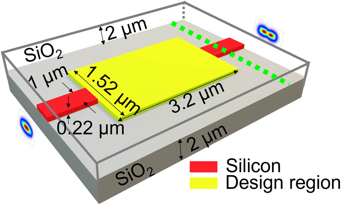
    Fig. 1. Illustration of the dimensions of the input and output waveguides (in red) and the design region (in yellow) for the TE0 to TE1 mode converter.
    (a) Initial and optimized mode converters for gray scale optimization strategies (note that wc=0 corresponds to a gray scale optimization), baseline, and with energy constraint coefficients wc of 0.1, 0.3, 0.5, 0.7, and 0.9; (b) insertion loss and binarization level as a function of the energy constraint coefficient parameter wc (horizontal purple dashed line, IL performance of the baseline design; horizontal light blue dashed line, binarization level of the baseline design); energy intensity distribution for the optimized designs (c) without and (d) with energy constraint.
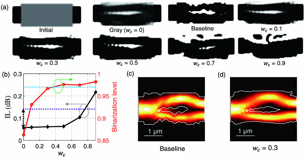
    Fig. 2. (a) Initial and optimized mode converters for gray scale optimization strategies (note that wc=0 corresponds to a gray scale optimization), baseline, and with energy constraint coefficients wc of 0.1, 0.3, 0.5, 0.7, and 0.9; (b) insertion loss and binarization level as a function of the energy constraint coefficient parameter wc (horizontal purple dashed line, IL performance of the baseline design; horizontal light blue dashed line, binarization level of the baseline design); energy intensity distribution for the optimized designs (c) without and (d) with energy constraint.
    Optical image of the test structures for characterizing the mode converter in terms of (a) IL performance and (b) cross talk performance; (c) SEM images for the fabricated design of the baseline (left) and energy constraint strategies (right); (d) measured IL and XT for the mode converter designed by the baseline (solid line) and energy constraint strategies (dashed line); right part shows the zoom in version of the measured IL performance.
    Fig. 3. Optical image of the test structures for characterizing the mode converter in terms of (a) IL performance and (b) cross talk performance; (c) SEM images for the fabricated design of the baseline (left) and energy constraint strategies (right); (d) measured IL and XT for the mode converter designed by the baseline (solid line) and energy constraint strategies (dashed line); right part shows the zoom in version of the measured IL performance.
    (a) Illustration of the dimensions of the input and output waveguides (in red) and the design region (in yellow) for the 1310 nm/1550 nm wavelength duplexer; (b) illustration of the wavelength points at which the optimization is conducted for the 1310 nm and 1550 nm channels, respectively.
    Fig. 4. (a) Illustration of the dimensions of the input and output waveguides (in red) and the design region (in yellow) for the 1310 nm/1550 nm wavelength duplexer; (b) illustration of the wavelength points at which the optimization is conducted for the 1310 nm and 1550 nm channels, respectively.
    (a) Initial and optimized 1310 nm/1550 nm wavelength duplexer layouts for different strategies (note that wc=0 corresponds to the gray scale optimization); (b) energy intensity distribution inside the optimized designs for baseline (left) and the case with energy constraint coefficient wc=0.3 (right) (red, 1550 nm; cyan, 1310 nm); simulated transmission spectrum results from (c) baseline optimization and (d) the case with energy constraint coefficient wc=0.3.
    Fig. 5. (a) Initial and optimized 1310 nm/1550 nm wavelength duplexer layouts for different strategies (note that wc=0 corresponds to the gray scale optimization); (b) energy intensity distribution inside the optimized designs for baseline (left) and the case with energy constraint coefficient wc=0.3 (right) (red, 1550 nm; cyan, 1310 nm); simulated transmission spectrum results from (c) baseline optimization and (d) the case with energy constraint coefficient wc=0.3.
    Simulated transmission spectrum for (a) baseline optimization and (b) the case with energy constraint coefficient wc=0.3 under ±10 nm fabrication error. For clarity of the figure, the data for the nominal designs are not shown here.
    Fig. 6. Simulated transmission spectrum for (a) baseline optimization and (b) the case with energy constraint coefficient wc=0.3 under ±10  nm fabrication error. For clarity of the figure, the data for the nominal designs are not shown here.
    Histogram of minimum feature size ranges for (a) 15 baseline optimization runs and (b) 15 runs with an energy constraint coefficient of wc=0.3; overlap of all 15 simulated transmission spectra for (c) baseline optimization and (d) with energy constraint coefficient wc=0.3 under ±10 nm fabrication imperfection.
    Fig. 7. Histogram of minimum feature size ranges for (a) 15 baseline optimization runs and (b) 15 runs with an energy constraint coefficient of wc=0.3; overlap of all 15 simulated transmission spectra for (c) baseline optimization and (d) with energy constraint coefficient wc=0.3 under ±10  nm fabrication imperfection.
    SEM images of eight fabricated 1310 nm/1550 nm wavelength duplexers optimized from different random start parameters. Top row, devices from baseline optimization strategy; bottom row, corresponding devices from energy constraint optimization strategy.
    Fig. 8. SEM images of eight fabricated 1310 nm/1550 nm wavelength duplexers optimized from different random start parameters. Top row, devices from baseline optimization strategy; bottom row, corresponding devices from energy constraint optimization strategy.
    Measured and normalized transmission spectrum of the fabricated 1310 nm/1550 nm wavelength duplexer under ±10 nm and 0 nm boundary bias for (a) baseline, (b) energy constraint optimization; filtered transmission spectrum of the results presented in (a) and (b) for (c) baseline, (d) energy constraint optimization.
    Fig. 9. Measured and normalized transmission spectrum of the fabricated 1310 nm/1550 nm wavelength duplexer under ±10  nm and 0 nm boundary bias for (a) baseline, (b) energy constraint optimization; filtered transmission spectrum of the results presented in (a) and (b) for (c) baseline, (d) energy constraint optimization.
    Measured, normalized, and smoothed transmission spectra of the fabricated 1310 nm/1550 nm wavelength duplexers under different ±10 nm boundary bias for the 15 designs optimized from different random initial parameters for (a) baseline and (b) energy constraint optimization.
    Fig. 10. Measured, normalized, and smoothed transmission spectra of the fabricated 1310 nm/1550 nm wavelength duplexers under different ±10  nm boundary bias for the 15 designs optimized from different random initial parameters for (a) baseline and (b) energy constraint optimization.
    (a) Illustration of the dimensions of the input and output waveguides (in red) and the design region (in yellow) for the CWDM demultiplexer. (b) Illustration of the wavelength points at which the optimization is conducted for the CH1, CH2, and CH3, respectively.
    Fig. 11. (a) Illustration of the dimensions of the input and output waveguides (in red) and the design region (in yellow) for the CWDM demultiplexer. (b) Illustration of the wavelength points at which the optimization is conducted for the CH1, CH2, and CH3, respectively.
    (a) Optimized CWDM demultiplexer layouts for different strategies (note that wc=0 corresponds to the gray scale only optimization); (b) corresponding energy distribution inside the optimized designs with different energy constraint coefficients; (c) corresponding simulated transmission spectrum for the optimized designs with different parameters wc.
    Fig. 12. (a) Optimized CWDM demultiplexer layouts for different strategies (note that wc=0 corresponds to the gray scale only optimization); (b) corresponding energy distribution inside the optimized designs with different energy constraint coefficients; (c) corresponding simulated transmission spectrum for the optimized designs with different parameters wc.
    Simulated transmission spectrum of the optimized CWDM demultiplexers under different ±10 nm and 0 nm boundary biases optimized with different energy constraint coefficients for CH1 (left), CH2 (middle) and CH3 (right), (a) wc=0.5, (b) wc=0.7, and (c) wc=0.9, respectively.
    Fig. 13. Simulated transmission spectrum of the optimized CWDM demultiplexers under different ±10  nm and 0 nm boundary biases optimized with different energy constraint coefficients for CH1 (left), CH2 (middle) and CH3 (right), (a) wc=0.5, (b) wc=0.7, and (c) wc=0.9, respectively.
    (a) SEM images of the fabricated CWDM demultiplexer for wc=0.5,0.7,0.9; (b) zoom-in SEM images with the overlap of the desired boundary; (c)–(e) measured transmission spectrum of the nominal demultiplexers optimized with energy constraint coefficients wc=0.5,0.7,0.9.
    Fig. 14. (a) SEM images of the fabricated CWDM demultiplexer for wc=0.5,0.7,0.9; (b) zoom-in SEM images with the overlap of the desired boundary; (c)–(e) measured transmission spectrum of the nominal demultiplexers optimized with energy constraint coefficients wc=0.5,0.7,0.9.
    Measured transmission spectrum of the fabricated CWDM demultiplexers under different ±10 nm and 0 nm boundary biases optimized with different energy constraint coefficients for CH1 (left), CH2 (middle), and CH3 (right), respectively, (a) wc=0.5, (b) wc=0.7, and (c) wc=0.9.
    Fig. 15. Measured transmission spectrum of the fabricated CWDM demultiplexers under different ±10  nm and 0 nm boundary biases optimized with different energy constraint coefficients for CH1 (left), CH2 (middle), and CH3 (right), respectively, (a) wc=0.5, (b) wc=0.7, and (c) wc=0.9.
    Measured spectrum shifts due to ±10 nm etching changes as a function of the energy constraint coefficient wc for CH1 (blue), CH2 (green), and CH3 (red).
    Fig. 16. Measured spectrum shifts due to ±10  nm etching changes as a function of the energy constraint coefficient wc for CH1 (blue), CH2 (green), and CH3 (red).
    Top view illustration of filtering and projection on a predefined design region (dash blue line): (a) design variable of material distribution ρ ranging between 0 and 1, (b) the variable of material distribution ρ˜ after filtering using a hat-shaped filter h(x,y) shown in the insert, (c) the variable of material distribution ρ¯, which is the projection of the filtered material distribution ρ˜. The inset for projection shows how changing β will help binarize the structure.
    Fig. 17. Top view illustration of filtering and projection on a predefined design region (dash blue line): (a) design variable of material distribution ρ ranging between 0 and 1, (b) the variable of material distribution ρ˜ after filtering using a hat-shaped filter h(x,y) shown in the insert, (c) the variable of material distribution ρ¯, which is the projection of the filtered material distribution ρ˜. The inset for projection shows how changing β will help binarize the structure.
    (a) Illustration of continuous distribution from optimization; (b) illustration of the GDS transferring process using Eq. (A15); (c) illustration of boundary bias erosion (−10 nm), normal (0 nm), and dilation (+10 nm) at the cross section position; (d) and (e) zoom-in illustration for part of the design boundary.
    Fig. 18. (a) Illustration of continuous distribution from optimization; (b) illustration of the GDS transferring process using Eq. (A15); (c) illustration of boundary bias erosion (10  nm), normal (0 nm), and dilation (+10  nm) at the cross section position; (d) and (e) zoom-in illustration for part of the design boundary.
    Ref.Footprint (μm2)BW (nm)XT (dB)IL (dB)Time (h)Hardware
    [41]4×4100–22.00.3436Intel Core i7-8700 CPU
    [42]4×1.640–9.11.3450Intel Xeon E5 2697 v3 CPU
    This work (baseline)3.2×1.52100–23.00.344NVidia V100 GPU
    This work (wc=0.3)3.2×1.52100–26.70.184NVidia V100 GPU
    Table 1. Comparison of the Performance of Mode Converters with the Previous Reported Inversely Designed Mode Converters/Exchangers
    Ref.Footprint (μm2)3-dB BW O/C Band (nm)XT (dB)IL O/C Band (dB)Time (h)Hardware
    [2]2.8×2.8100/170–111.8/2.436NVidia GTX Titan GPU
    This work (baseline)3.2×3150/170–151/1.512NVidia V100 GPU
    This work (wc=0.3)3.2×3120/150–150.75/1.512NVidia V100 GPU
    Table 2. Comparison of the Performance of the 1310 nm/1550 nm Wavelength Duplexer with Previous Reported Inversely Designed 1310 nm/1550 nm Wavelength Duplexers
    ChannelsSpectrum Shifts (nm)
    SimulatedMeasured
    wc=0.5wc=0.7wc=0.9wc=0.5wc=0.7wc=0.9
    CH1422819402720
    CH2503421603221
    CH3353023363021
    Table 3. Simulated and Measured Spectrum Shifts for CH1, CH2, and CH3 under Different Energy Constraint Coefficients for ±10 nm Boundary Biases
    Ref.Footprint (μm2)1-dB/3-dB BW (nm)XT (dB)IL (dB)Channel Spacing (nm)Time (h)Hardware
    [32]5.5×4.5Not reported–11.02.824060NVidia GTX Titan GPU
    This work (wc=0.5)6.2×5.419/32–19.11.95048NVidia V100 GPU
    This work (wc=0.7)6.2×5.430/43–16.31.25048NVidia V100 GPU
    This work (wc=0.9)6.2×5.430/47–11.51.85048NVidia V100 GPU
    Table 4. Comparison of the Performance of the CWDM Demultiplexers with Previous Reported Inversely Designed CWDM Demultiplexers
    Guowu Zhang, Dan-Xia Xu, Yuri Grinberg, Odile Liboiron-Ladouceur. Experimental demonstration of robust nanophotonic devices optimized by topological inverse design with energy constraint[J]. Photonics Research, 2022, 10(7): 1787
    Download Citation