
Yaqian Qian, Shushan Qiao, Rongqiang Yang. Variation tolerance for high-speed negative capacitance FinFET SRAM bit cell[J]. Journal of Semiconductors, 2020, 41(6): 062403
- Journal of Semiconductors
- Vol. 41, Issue 6, 062403 (2020)
Abstract
1. Introduction
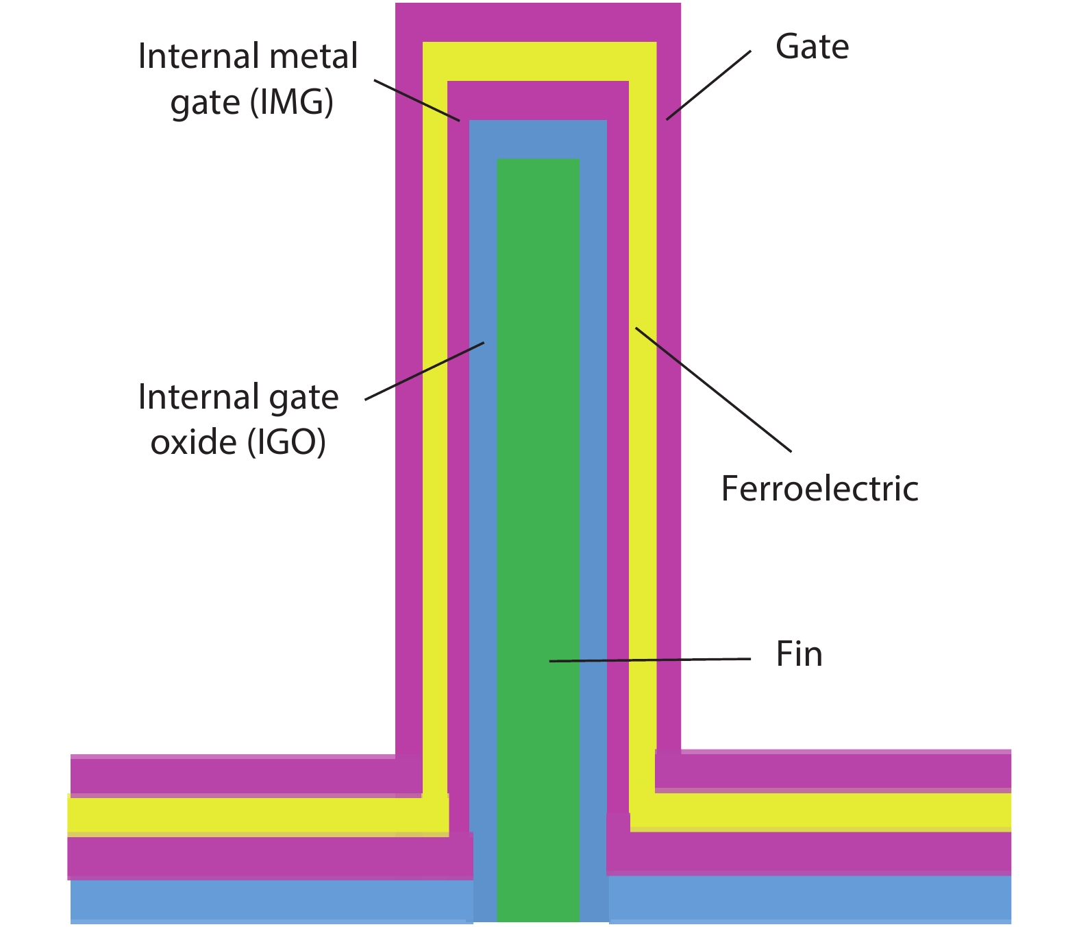
The structure of NC-FinFETs is almost the same as FinFETs, but the NC layer is positioned between the gate and internal gate, whose structure is MFMIS (metal–ferroelectric–metal–insulator–semiconductor) as shown in Fig. 1[
![]()
Figure 1.(Color online) the structure of NC-FinFET.
![]()
Figure 2.(Color online) The subthreshold swing improved by NC compared to the baseline.
In this paper, we study the effects of the variation of ferroelectric material (thickness, polarization), FinFET critical physical parameters (fin number, channel length) and some ambient factors (working temperature, supply voltage) on the performance of NC-FinFET SRAM with high read speed.
2. Device structure and simulation scheme
Fig. 3 is a schematic of a traditional 6T bit-cell consisting of NC-FinFETs. This paper will study the performance of SRAM based on the above structure, how to analyze the internal factors and find a better balance will be carried out through the simulation process of Fig. 4. Firstly, the ferroelectric materials commonly used in NCFETs are perovskite ferroelectrics. These materials have good stability. The local temperature is about 500 °C. Therefore, even at high temperatures of 125 °C, The negative capacitance characteristics remain the same, and the performance will not abruptly change due to this temperature. Static noise margin (SNM) is the term used to determine the stability of the SRAM cells. The SNM is the tolerance of the maximum noise voltage for the cross inverters output nodes and the minimum amount of noise to ensure the state is maintained[
![]()
Figure 3.The schematic of traditional 6T SRAM-cell.
![]()
Figure 4.The simulation flow chart for analysis the performance variation for the 6T SRAM, and the compact model is the BSIM-CMG cooperating L-K equations.
Even under the same process, n-type and p-type transistors present different performances, especially the threshold voltage (VT). Fig. 5 confirms the above conclusions. It can be seen that as the thickness of the ferroelectric increases, the VT mismatch between the two transistors becomes more serious. The threshold voltage of the ferroelectric material is negative, so the VT of a NC-FinFET will be lower compared to the baseline FinFET. The threshold voltage of the device is the minimum voltage required to turn on the transistor, which is closely related to the gate control capability of the device itself. The study of this work is based on the actual taped-out FinFET data, the mismatch between n-type and p-type transistors is small, but as Tfe increases, the VT variation degree of the two is not consistent due to the difference of the carrier transport mechanism between them. The grid-control capability of n-type NC-FinFETs will become weaker with the increase of ferroelectric thickness, while the p-type will be relatively slow. So, as the Tfe increases, the VT mismatch will increase. In order to observe the tolerance variation on cell level, the same change will be applied for the whole SRAM cell. To evaluate the stability of NC-FinFET SRAM cells, first of all, under a fixed FinFET baseline and working environment, by changing the ferroelectric material the single transistor showed that as the thickness of the ferroelectric decreased, the negative DIBL phenomenon will be more apparent. A suitable choice of polarization is difficult to a certain extent, so in this work we refer to the parameters in paper[
![]()
Figure 5.(Color online) The
3. Results and discussion
Followed by all the above simulation flows, some phenomena can be observed from the graphs. Firstly, we will study the integration of ferroelectric material and basic FinFET even though the polarization is difficult to extract from the figure, while the recently proposed SPICE model of ferroelectric material in Ref. [11] utilizes a very complex circuit to express the nonlinear dependence of VFE upon polarization (P). P is self-consistently equal to gate charge (Qg) of the FinFET. Hence, the model is independent of FinFET parameters[
![]()
Figure 6.(Color online) (a) Read speed, (b) leakage, (c) SNM, and (d) WM of NC-FinFET SRAM influenced by the thickness of ferroelectric material.
Refs. [14, 15] explain that the CFE should be a little larger than Cbaseline, and the large discrepancy will lead to a mismatch between negative capacitance and FinFET capacitance, while the coefficient is fixed, so the thicker the ferroelectric material becomes, more serious the mismatch problem will be. The work function is associated with the gate structure, so the relationship between ferroelectric and baseline needs further research. Furthermore, the reliability is still unclear.
Secondly, having fixed the parameters of ferroelectric material, in this part, we have analyzed the critical metrics of the baseline. As with the above operation, all the changes are the same for the whole SRAM cell. Increasing the fin number (Nfin) of the NC-SRAM cell, the influences basically conforms to the baseline. In detail, read speed is remarkably improved since the increase of Nfin contributes to the current, as shown in Fig. 7(a). Meanwhile, in Fig. 7(b), the leakage problem gets worse because increasing the fin number is equivalent to making the width longer, resulting in the leakage path being broadened. Some other metrics are shown in Figs. 7(c) and 7(d), the change of SNM and WM is not evident, but we can still see that when the fin number is only 1, both of them are better. The tendency is not parallel to the baseline, so the fin number of NC-FinFET should harmonize with the baseline SRAM cell. Another parameter: channel length (Lg) is also vital to the NC-FinFET SRAM cell. In principle, the read speed will slow down while the Lg increases for the reason that the voltage and current controlled by gate is enhanced in a short-channel device. The NC-SRAM cell optimizes the read speed well obeying the above rules. In the cell level, the leakage problem is presented in Fig. 8(b), the leakage problem is gradually improved because the short channel will lead to larger junction leakage. The more detail causes can be deduced from the formula[
![]()
Figure 7.(Color online) (a) Read speed, (b) leakage, (c) SNM, and (d) WM of NC-FinFET SRAM influenced by the fin number of baseline with fixed FE thickness 3 nm.
![]()
Figure 8.(Color online) (a) Read speed, (b) leakage, (c) SNM, and (d) WM of NC-FinFET SRAM influenced by the channel length of baseline with one fin.
In the formula, the factor most severely influenced by length is Ijunction. So, to some extent, the correspondence between the ferroelectric material and baseline mainly account for the leakage, which means the channel length determines the static power of the cell. From Fig. 8(c), the SNM is almost maintained under the same voltage, but a little abnormal phenomenon occurs when the supply voltage is 0.8 V. To account for this, the SNM can be expressed[
In this paper, the size of the PD, PU and PG are all the same, so r and q are equal to 1. To analyze the influence of the channel length for SNM, the VDD will be fixed to 0.8 V, then we get following formula:
The conclusion can be drawn that in this case, SNM has the same change tendency with the VT, while VT is almost determined by channel length. So the VT reflects the SNM. Conversely, the WM drops mildly. From all of above, the channel length is not only important to the baseline SRAM but also sensitive to the NC-FinFET SRAM. An appropriate channel length maybe the key factor for the whole NC-FinFET SRAM. Apart from that, in all figures the supply voltage also affects the performance. Most of the metrics conform to normal rules except SNM and WM under special cases. The range of supply voltages ensuring the NC-FinFET SRAM works correctly will be discussed after fixing all the above parameters with best choice. From all the graphics, the best voltage for the cell can be chosen between 0.5 to 0.7 V, making low power significant. Fig. 9 presents the temperature infection. It has been mentioned the structure chosen in this article is MFMIS. The interconnection between the metallic and ferroelectric layers is based on the principle of self-continuity of charge, because the ferroelectric layer and the metal layer share only charge, but the material itself is not compatible. When the temperature is 125 °C, the ferroelectric remains stable and the metal layer will not migrate. Therefore, under reasonably high temperature, the device itself is in a stable state. Read speed is almost flat while static leakage abruptly rises under higher temperature. The SNM declines slightly while WM increases gently.
![]()
Figure 9.(Color online) (a) Read speed, (b) leakage, (c) SNM, and (d) WM of NC-FinFET SRAM influenced by temperature with one fin and supply voltage ranges from 0.5 to 0.7 V.
4. Conclusion
Based on an ordinary and reasonably proper SPICE model of ferroelectrics, the performance of a NC-FinFET SRAM cell is presented. We discussed the variation tolerance for the NC-FinFET SRAM cell. A small Tfe ranging from 1 to 3 nm exhibits a better performance while sacrificing little speed. Small Nfin is the better choice in this paper due to the fact that SNM and WM barely change when the fin number increases but the leakage problem becomes serious. Channel length is limited to within 6 nm, due to the fact that trade-off among leakage, SNM and WM cannot be eliminated, except under small channel length, and the read speed and WM is perfect while the leakage problem can be cleaned up by making NC-FinFET SRAM work under a low supply voltage. Therefore, a reasonable supply voltage range is 0.5 to 0.7 V. This work utilizes its low power advantage meanwhile ensuring performance. Considering the application in industry, both low and high temperatures can be tolerated, ranging from –40 to 125 °C which is the detection range commonly used in process.
Acknowledgements
This work was supported in part by the University of Chinese Academy of Science and SMIC
References
[1] K Li, P Chen, T Lai et al. Sub-60mV-swing negative-capacitance FinFET without hysteresis. IEEE International Electron Devices Meeting (IEDM), 22(2015).
[2] C Lin, A I Khan, S Salahuddin et al. Effects of the variation of ferroelectric properties on negative capacitance FET characteristics. IEEE Trans Electron Devices, 63, 21972199(2016).
[3] S Khandelwal, A I Khan, J P Duarte et al. Circuit performance analysis of negative capacitance FinFETs. IEEE Symposium on VLSI Technology, 1(2016).
[4] E Ko, H Lee, Y Goh et al. Sub-60-mV/decade negative capacitance FinFET with sub-10-nm hafnium-based ferroelectric capacitor. IEEE J Electron Devices Soc, 5, 306309(2017).
[5] H Ota, K Fukuda, T Ikegami et al. Perspective of negative capacitance FinFETs investigated by transient TCAD simulation. IEEE International Electron Devices Meeting (IEDM), 15(2017).
[6] S Khandelwal, J P Duarte, A I Khan et al. Impact of parasitic capacitance and ferroelectric parameters on negative capacitance FinFET characteristics. IEEE Electron Device Lett, 38, 142144(2017).
[7] H Banga, D Agarwal. Single bit-line 10T SRAM cell for low power and high SNM. International Conference on Recent Innovations in Signal processing and Embedded Systems (RISE), 433(2017).
[8] G Zhang, Y Li, S F Yu. Techniques to improve read noise margin and write margin for bit-cell of 14 nm FINFET node. China Semiconductor Technology International Conference, 1(2015).
[9] K T Chen, S S Gu, M H Lee. Ferroelectric HfZrO
[10] A Aziz, S Ghos, S Datta et al. Physics-based circuit compatible SPICE model for ferroelectric transistors. IEEE Electron Device Lett, 37, 805808(2016).
[11] V Kumar, R K Shrivatava, M M Padaliya. A temperature compensated read assist for low
[12] Y Li, K Yao, G S Samudra. Delay and power evaluation of negative capacitance ferroelectric MOSFET based on SPICE model. IEEE Trans Electron Devices, 64, 24032408(2017).
[13] T Dutta, G Pahwa, A R Trivedi et al. performance evaluation of 7-nm node negative capacitance FinFET-based SRAM. IEEE Electron Device Lett, 38, 1161(2017).
[14] G Pahwa, T Dutta, A Agarwal et al. Analysis and compact modeling of negative capacitance transistor with high on-current and negative output differential resistance —Part I: model description. IEEE Trans Electron Devices, 63, 4981(2016).
[15] G Pahwa, T Dutta, A Agarwal et al. Analysis and compact modeling of negative capacitance transistor with high on-current and negative output differential resistance—Part II: model validation. IEEE Trans Electron Devices, 63, 4986(2016).
[16] Q Dong, Y N Ma, H Chen et al. A novel method for accurate measurement and decoupling of SRAM standby leakage. IEEE 11th International Conference on Solid-State and Integrated Circuit Technology, 1(2012).
[17] G Prasad, R Kusuma. Statistical (M-C) and static noise margin analysis of the SRAM cells. Students Conference on Engineering and Systems (SCES), 1(2013).

Set citation alerts for the article
Please enter your email address
© Copyright 2018-2021 | Chinese Laser Press. All Rights Reserved 沪ICP备15018463号-20