
Yuwei Cai, Zhaohao Zhang, Qingzhu Zhang, Jinjuan Xiang, Gaobo Xu, Zhenhua Wu, Jie Gu, Huaxiang Yin. Investigation of time domain characteristics of negative capacitance FinFET by pulse-train approaches[J]. Journal of Semiconductors, 2021, 42(11): 114101
- Journal of Semiconductors
- Vol. 42, Issue 11, 114101 (2021)
Abstract
1. Introduction
Negative capacitance field-effect transistors (NC FETs) have been widely investigated in recent years as a powerful alternative for low-power and high-performance circuits due to their ultra-steep subthreshold characteristics and compatibility with traditional complementary metal–oxide–semiconductor (CMOS) processes[
In this paper, based on our fabricated high-performance HZO NC FinFET, two measurement platforms based on an oscilloscope and arbitrary wave function generator were built in order to characterize the transient characteristics of the NC FinFET. The conventional resistive load inverter test scheme can characterize the transient characteristics of the device, however, there are significant high-frequency limitations, and the frequency domain can be characterized within 100 kHz. Furthermore, the transient response in the higher frequency domain can be measured by using an oscilloscope connected directly to the source of the device as a ground. The scheme eliminates the effect of load resistance and can measure the transient current response at pulse widths as low as 5 ns.
2. Experiment and method
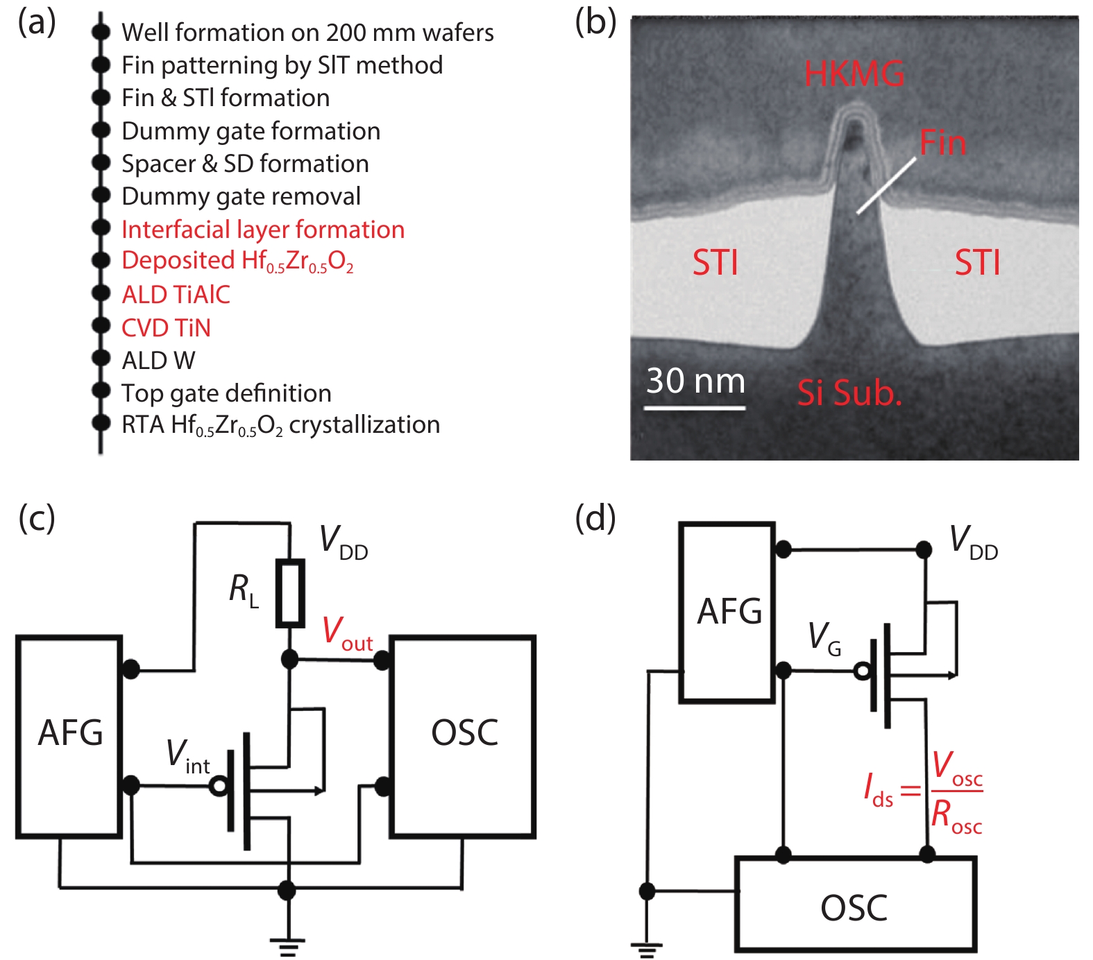
Fig. 1(a) shows the fabrication flow of the HZO NC FinFET, which is similar to our previous work[
![]()
Figure 1.(Color online) (a) The fabrication flow of the fabrication of NC FinFET. (b) Cross-sectional TEM image of the NC FinFET device. (c) Schematic diagram of the resistive load inverter characterization single-transistor frequency characteristics test circuit. (d) Schematic diagram of the optimization measurement scheme.
Here the internal resistance of the oscilloscope selects 1 MΩ, which is much larger than the on resistance of the transistor, so the shunt effect of the oscilloscope could be ignored. The frequency characteristics of the transistor can be studied by monitoring the change in Vout, when keeping the drain voltage VDD constant, and only changing the pulse width of the applied gate signals. Theoretically, if high-frequency characteristics of the device deteriorate as the pulse width decreases, the on-current of the device will decrease under the same gate and drain voltages. Meanwhile, the corresponding Vout will increase and the high-frequency characteristics can be characterized in this way. Furthermore, the optimization of the measurement scheme is shown in Fig. 1(d) and will be explained later in detail.
3. Results and discussion
3.1. Frequency response of NC FinFETs based on load resistance inverter measurements
In the experiment, the applied gate pulse amplitude is set to 0.8 V, the pulse width was adjusted according to the actual experimental needs (the drain voltage VDD = 0.8 V, RL = 100 kΩ). Fig. 2 shows the measured Vout in our experiment with different frequencies. As shown in Fig. 2(a), the output signal is a rectangular wave with an amplitude of 0.26 V under an applied VGS of 1 ms pulse width (corresponding to frequency 0.5 kHz), and there is large discrimination between the high and low levels of the output voltage. However, the output signal is no longer a complete rectangular pulse signal when the gate pulse frequency increases to 5 kHz (Fig. 2(b)). Therefore, the frequency characteristics of the device may be studied by changing the gate pulse frequency in a not high frequency domain.
![]()
Figure 2.(Color online) Real-time output data of the load-resistance based inverter measurement, with the gate pulse width (a) 1 ms, and (b) 10
Fig. 3 shows the measured output voltage as a function of gate pulse frequencies and the device used is a conventional NMOS FinFET. When the gate pulse frequency is higher than 100 kHz, the output voltage (Vout) began to gradually increase, indicating that the on-state current of the device gradually reduced with pulse width below 10 μs. The results indicating the performance of the device may degrade at high-frequency conditions. After analyzing the specific data, we suspect that the variation of output voltage in this test scheme may be mainly the effect of the capacitive resistance of the load resistor rather than the degradation of device performance, because our manufacture conventional devices with high frequency performance at least in the MHz frequency domain theoretically. Therefore, to test our suspicionsa, a 5 V pulse signal was sent on the load resistance directly connected to the oscilloscope in varies frequencies. The test results show that the signal on the oscilloscope exhibits serious distortion when the applied pulse width is shorter than 10 μs, as shown in Figs. 4(a) and 4(b), respectively. So the measured results shown using the above resistor-loaded inverter do not truly reflect the high-frequency performance of the transistor. In addition, the load resistor resistance in this scheme requires the load resistor to have good high-frequency characteristics and comparable to the device on-resistance or much larger than the on-resistance (generally several tens of kΩ level). Then the oscilloscope shows the voltage of the device in the on state and the voltage in the off state will be obviously different.
![]()
Figure 3.(Color online) Experimentally measured output voltage as a function of the applied gate signal frequencies.
![]()
Figure 4.Waveforms of different frequencies displayed directly on the oscilloscope after resistive loading, (a)10 kHz and (b) 100 kHz.
A large resistance value and good high-frequency performance of the resistor could not be achieved (a high-frequency test in general load resistance value of 50 Ω) because the larger the impedance value, the greater the capacitive resistance. Therefore, the test scheme needs to be optimized in order to further study the high-frequency performance based on a single transistor.
3.2. Frequency response with optimization measurement for single-NC Fin-FETs
In order to eliminate the influence of load resistance effect, an optimized measurement scheme based on a single transistor was proposed and carried out, as shown in Fig. 1(d). In this scheme, both the signal generator and oscilloscope internal resistance were set to 50 Ω impedance, and the oscilloscope was directly connected to the source of the device, i.e., connecting the source of the device directly to the 50 Ω impedance channel of the oscilloscope, and the drain current can be calculated directly by the following equation:
R0 = 50 Ω represents the impedance of the oscilloscope. This scheme excludes the influence of load resistance and sets the waveform of the pulse string loaded on the gate to take a point every 0.05 V from 0.05 to 1 V, with a total of 20 pulses in one pulse string cycle. The width of each pulse can be controlled by setting the individual pulse string time, and then the Id–Vg curves of different amplitudes and pulse widths are measured out. The sub-threshold slope (SS), hysteresis, threshold voltage (Vt) and drain-induced barrier lowering (DIBL) can then be extracted for the corresponding pulse width to fully analyze the frequency characteristics of the device. The measured single-transistor real-time results were directly carried out, shown in Fig. 5. Under the 1 μs pulse width, when the gate voltage is greater than 0.3 V (a PMOS device used here, the on-state voltage is negative voltage region) we can accurately extract the on-state current. However, when the gate voltage is lower than 0.3 V, the on-state current is too small (at this time, the nA level current is about 0.5 μV magnitude on the oscilloscope), and the oscilloscope vertical axis resolution is not enough (resolution has been adjusted to the highest). Therefore, the program can be studied by measuring the on-state IDS to its frequency characteristics. The test conditions are set to VGS = VDD = 1 V for NMOS (–1 V for PMOS), and the gate pulse widths are 10 ms, 1 ms, 100 μs, 10 μs, 1 μs, and only the variation of the IDS in the on-state with frequency is studied.
![]()
Figure 5.(Color online) The measured real-time pulse train on-current of single-transistor.
Figs. 6(a) and 6(b) show the experimentally measured transient pulse current at pulse widths of 10 ms and 1 μs, when VGS = VDD = –1 V. The frequency characteristics of the device by characterizing the variation of the pulse current with the gate pulse width were characterized. The results show that the pulse width is as short as the order of μs, and the measured current signal is still very clear, which is more credible than those of the resistive load test scheme.
![]()
Figure 6.(Color online) Measured transient currents of the single transistor, (a) with 10 ms pulse width, (b) with 1
Fig. 6(c) shows the variation of the transient on-state current with pulse width measured in the experiment. It can be seen that with the gradual decrease of the gate pulse width, the on-state current of the device does not change significantly in the frequency range of 1 MHz, for all three gate voltage conditions. The results show that the device in the 1 MHz frequency range and the on-state current does not affect the frequency, which indicated that the NC FinFET can work at 1 MHz frequency and the on-state current does not significantly degrade. Nonetheless, the scheme is indeed also not a complete characterization of the IDS–VGS curve at high frequencies, but it can also characterize the device's high-frequency characteristics to some extent, because the on-current does not vary with the gate frequency. Therefore, we continued to reduce the pulse width on the basis of 1 MHz and studied in depth the variation of the on-state current of a single NC FinFET with a minimum pulse width measured to 5 ns.
Fig. 7 shows the experimentally measured on-current with a pulse width of 100 ns. The discrimination between high and low levels is obvious under this test scheme, and the off-state noise is small, so the transient on-current of the device can be clearly measured.
![]()
Figure 7.(Color online) Real-time test results of on-state
Fig. 8 summarizes the frequency test results for NMOS and PMOS devices, the red and blue curves represent NC FinFETs and conventional HfO2 FinFETs, respectively. The results show that the on-current of both devices does not vary with the gate signal pulse width. However, the on-current of both devices shows a trend to become larger with the gate voltage pulse width gradually below 100 ns, which seems to contradict the theory of conventional MOSFETs. In fact, the FinFET gate interface layer is not an ideal interface, including some defects and traps, and the phenomenon can be explained by the fast trap effect[
![]()
Figure 8.(Color online) Experimentally measured variation of the on-state current with pulse width for NC FinFET and conventional FinFET. (a) NMOS. (b) PMOS.
More importantly, under the same conditions, the measured on-state current of the NC FinFET is consistently greater than those of the conventional FinFET (about 80% @ NMOS and almost equal @ PMOS), and a gate voltage pulse width of 5 ns is demonstrated using this approach, indicating that the NC FinFET also has an advantage over the conventional device in terms of drive current for high frequency applications, which is may be attributed to the inherent charge gain effect of the ferroelectric material[
4. Conclusion
In summary, the frequency characteristics based on single-NC FinFET are systematically investigated by two self-built test schemes. The conventional resistive load invertor test solution can only characterize the frequency characteristics in the low-frequency domain. However, the optimized solution test scheme of single transistor shows that the on-state current does not significantly change in the 1 MHz frequency domain. Further high-frequency test results show that NC FinFETs and conventional FinFETs start to show a trend of larger on-currents when the gate voltage pulse width is less than 100 ns, which is attributed to the defect effect of the device interface layer. Furthermore, NC FinFETs exhibit a larger on-current than that of the conventional FinFETs, which is related to the charge gain of ferroelectric materials. The overall experimental results show that NC FinFETs have a high-frequency performance in terms of on-state current that is not weaker than that of conventional FinFETs, and the current driving capability is better than that of conventional devices, which is an important impetus for future research on the high-frequency characteristics of NC FinFETs.
Acknowledgements
This project was supported in part by the Science and Technology program of Beijing Municipal Science and Technology Commission under grant Z201100006820084, in part by the National Natural Science Foundation of China (NSFC) under grants 92064003, 61904194, 91964202 and 61874135, in part by the Youth Innovation Promotion Association, Chinese Academy of Sciences under grants Y9YQ01R004 and Y2020037, in part by the Opening Project of Key Laboratory of Microelectronic Devices and Integrated Technology, Institute of Microelectronics, Chinese Academy of Sciences under grants E0YS01X001 and E0290X03.
References
[1] S Salahuddin, S Datta. Use of negative capacitance to provide voltage amplification for low power nanoscale devices. Nano Lett, 8, 405(2008).
[2] A Rusu, G A Salvatore, D Jiménez et al. Metal-ferroelectric-meta-oxide-semiconductor field effect transistor with sub-60mV/decade subthreshold swing and internal voltage amplification. 2010 Int Electron Devices Meet, 16.3.1(2010).
[3] J R Zhou, G Q Han, N Xu et al. Experimental validation of depolarization field produced voltage gains in negative capacitance field-effect transistors. IEEE Trans Electron Devices, 66, 4419(2019).
[4] Q Q Huang, H M Wang, Y Zhao et al. New understanding of negative capacitance devices for low-power logic applications. 2019 China Semiconductor Technology International Conference (CSTIC), 1(2019).
[5] Y J Zhang, H Y Wang, L Zhang et al. Field-effect transistor memories based on ferroelectric polymers. J Semicond, 38, 111001(2017).
[6] H F Xu. Two dimensional analytical model for a negative capacitance double gate tunnel field effect transistor with ferroelectric gate dielectric. J Semicond, 39, 104004(2018).
[7] Z H Zhang, G B Xu, Q Z Zhang et al. FinFET with improved subthreshold swing and drain current using 3-nm ferroelectric Hf0.5Zr0.5O2. IEEE Electron Device Lett, 40, 367(2019).
[8] J R Zhou, G Q Han, Q L Li et al. Ferroelectric HfZrO
[9] Y W Cai, Q Z Zhang, Z H Zhang et al. Endurance characteristics of negative capacitance FinFETs with negligible hysteresis. IEEE Electron Device Lett, 42, 260(2021).
[10] Y X Li, R R Liang, J B Wang et al. Negative capacitance oxide thin-film transistor with sub-60 mV/decade subthreshold swing. IEEE Electron Device Lett, 40, 826(2019).
[11] J L Wang, D Wang, Q Li et al. Excellent ferroelectric properties of Hf0.5Zr0.5O2 thin films induced by Al2O3 dielectric layer. IEEE Electron Device Lett, 40, 1937(2019).
[12] J J Liao, B J Zeng, Q Sun et al. Grain size engineering of ferroelectric Zr-doped HfO2 for the highly scaled devices applications. IEEE Electron Device Lett, 40, 1868(2019).
[13] M J Tsai, P J Chen, P Y Peng et al. Atomic-level Analysis by synchrotron radiation and characterization of 2 nm, 3 nm, and 5 nm-thick Hf0.5Zr0.5O2 negative capacitance FinFET. 2019 Silicon Nanoelectronics Workshop (SNW), 1(2019).
[14] E J Nowak, I Aller, T Ludwig et al. Turning silicon on its edge [double gate CMOS/FinFET technology]. IEEE Circuits Devices Mag, 20, 20(2004).
[15] D Suh, J G Fossum. A physical charge-based model for non-fully depleted SOI MOSFET's and its use in assessing floating-body effects in SOI CMOS circuits. IEEE Trans Electron Devices, 42, 728(1995).
[16]
[17] K Chatterjee, A J Rosner, S Salahuddin. Intrinsic speed limit of negative capacitance transistors. IEEE Electron Device Lett, 38, 1328(2017).
[18] D Kwon, Y H Liao, Y K Lin et al. Response speed of negative capacitance FinFETs. 2018 IEEE Symposium on VLSI Technology, 49(2018).
[19] Z Krivokapic, U Rana, R Galatage et al. 14 nm Ferroelectric FinFET technology with steep subthreshold slope for ultra low power applications. 2017 IEEE Int Electron Devices Meet IEDM, 15.1.1(2017).
[20] K S Li, Y J Wei, Y J Chen et al. Negative-capacitance FinFET inverter, ring oscillator, SRAM cell, and
[21] M Kobayashi, N Ueyama, K Jang et al. Experimental study on polarization-limited operation speed of negative capacitance FET with ferroelectric HfO2. 2016 IEEE Int Electron Devices Meet IEDM, 12.3.1(2016).
[22] Z Yuan, S Rizwan, M Wong et al. Switching-speed limitations of ferroelectric negative-capacitance FETs. IEEE Trans Electron Devices, 63, 4046(2016).
[23] J R Zhou, J B Wu, G Q Han et al. Frequency dependence of performance in Ge negative capacitance PFETs achieving sub-30 mV/decade swing and 110 mV hysteresis at MHz. 2017 IEEE Int Electron Devices Meet IEDM, 15.5.1(2017).
[24]
[25]
[26]
[27] X Yu, B Chen, R Cheng et al. Fast-trap characterization in Ge CMOS using sub-1 ns ultra-fast measurement system. 2016 IEEE International Electron Devices Meeting (IEDM), 31.3.1(2016).
[28] J C Wong, S Salahuddin. Negative capacitance transistors. Proc IEEE, 107, 49(2019).


Set citation alerts for the article
Please enter your email address

© Copyright 2018-2021 | Chinese Laser Press. All Rights Reserved 沪ICP备15018463号-20