Abstract
Transition metal dichalcogenides are nowadays appealing to researchers for their excellent electronic properties. Vertical stacked nanosheet FET (NSFET) based on MoS2 are proposed and studied by Poisson equation solver coupled with semi-classical quantum correction model implemented in Sentaurus workbench. It is found that, the 2D stacked NSFET can largely suppress short channel effects with improved subthreshold swing and drain induced barrier lowering, due to the excellent electrostatics of 2D MoS2. In addition, small-signal capacitance is extracted and analyzed. The MoS2 based NSFET shows great potential to enable next generation electronics.Transition metal dichalcogenides are nowadays appealing to researchers for their excellent electronic properties. Vertical stacked nanosheet FET (NSFET) based on MoS2 are proposed and studied by Poisson equation solver coupled with semi-classical quantum correction model implemented in Sentaurus workbench. It is found that, the 2D stacked NSFET can largely suppress short channel effects with improved subthreshold swing and drain induced barrier lowering, due to the excellent electrostatics of 2D MoS2. In addition, small-signal capacitance is extracted and analyzed. The MoS2 based NSFET shows great potential to enable next generation electronics.1. Introduction
According to the 2021 International Roadmap for Devices and Systems (IRDS), gate-all-around (GAA) transistor will replace FinFET from 3 nm technology node, and it will apply to 1 nm technology node. In the next step, the goal of scaling down will be not only the decreased leakage but also the decreased power. And the 3D vertical architectures including 3D heterogeneous integration will become the mainstream technology to reduce power consumption. To continue Moore’s law, not only increasing circuit integration degree through device scaling down, but also power scaling and switching speed improvement, are necessary. Stacked NSFET is a promising candidate for future sub-3nm technology node because of better electrostatic integrity, short channel immunity and therefore better power scaling performance[1-3].
However, it is projected that, physical channel length, i.e., gate length (LG), would saturate around 12 nm due to worsening electrostatics. It can be inferred that planar size scaling by GAA structure is not able to sustain available performance. Accordingly, 2D semiconductors such as MoS2 has nowadays been regarded as promising alternative option for next generation semiconductor, for their excellent electronic properties[4-7] and regarded she promising candidate.
There are abundant researches on 2D MoS2 in recent years, due to its low dielectric constant, large band gap, valuable effective mass and dangling bond free surface[8]. These benefits can help achieve small leakage current and great switching characteristics. MoS2 transistors with ultra-scaled physical gate lengths and channel lengths realized by various cleverly designed experiments have been demonstrated and studied, exhibiting short channel effects (SCEs) more or less respectively. The inevitable degraded performances also emerge in MoS2 FET when device sizes scale down to nanometers[9, 10]. Contacts with 2D semiconductors fabricated by normal metal deposition process normally suffer from large contact resistance due to Fermi-level pinning effect, and experimental contaminations could also induce reduced 2D material quality in transfer process at the same time[11-14]. To investigate the potential advantages of MoS2 over bulk silicon (Si), keeping intrinsic material properties and assuming ideal contact are needed.
In the following, to capture the ideal ultimate performance of MoS2 FET, we will proceed as follows: First, we will begin with first-principle calculation for monolayer MoS2; then, the obtained physical parameters will be delivered to Sentaurus to replace original values in parameter file; finally, the comparison between the bulk and 2D materials is fully conducted and results are concluded.
2. Method
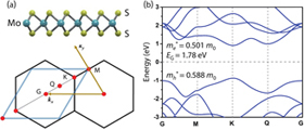
It has been reported that exporting physical parameters calculated by density functional theory (DFT) into Sentaurus tool is an effective method to match quantum approach while computational cost can be largely reduced[15]. Thus, DFT calculations based on Perdew-Burke-Ernzerhof (PBE) and generalized gradient approximation (GGA) functionals are conducted in the Quantum ATK 2020 code, to obtain reliable physical results. The real-space mesh cutoff is set at 55 Hartree, while the k-points sampling is set as 20 × 20 × 1. As in Fig. 1, the K and Q conduction band valleys with an energy difference can be observed. Then band gap (EG) of 1.78 eV, electron effective mass (me*) of 0.501 eV and hole effective mass (mh*) of 0.588 eV are extracted from the conduction band minimum (CBM) and valence band maximum (VBM).
Table Infomation Is Not Enable

Figure 1.(Color online) Energy band structures of MoS2 unit cell simulated with DFT showing the high symmetry points and a band gap EG = 1.78 eV.
Fig. 2(a) shows the schematic structure of NSFET. Corresponding device structure is built in Sentaurus Structure Editor (Fig. 2(b)). The width of nanosheet is set as 10 nm in all conditions, and channel thickness is 5 nm for Si and 0.65 nm for MoS2. To focus on the material itself, heavily doped source and drain in MoS2 are defined, and then the devices work in inversion mode. The underlap region and spacer retain the same for both scenarios.
Figure 2.(Color online) (a) Schematic diagram of a 3-stacked NSFET. (b) Bird eye view and cross-sectional view along the channel of simulated structure in Sentaurus. (c) Simulation framework of this work. (d) Calibration of transfer curves to experimental data in log and linear form. Experimental data are from a 3-stacked NSFET (LG = 10 nm).
The considered material properties contain the value of bandgap (EG), affinity (χ), mobility (μ), dielectric constant (ε), and the effective mass of hole (mh*) and electron (me*). These material physical parameters are delivered to the parameter file to simulate the transport characteristics (Fig. 2(c)).
Calibration to experimental Si-based 3-stacked NSFET with 12 nm LG was conducted at first by including Density Gradient model, Shockley Read Hall model and Oldslotboom model, as well as mobility models of High Field Saturation and Enormal[2, 16]. The transfer curves are then fitted with experimental data (Fig. 2(d)). Leveraging the calibrated physical model parameters, we studied the 2D MoS2 stacked NSFET and try to figure out the improvement brought by using the material parameters of MoS2. Table 1 summarizes the parameters used in this work.
3. Results and discussion
With the imported physical parameters of MoS2 modified, the transfer characteristics are compared in the same structure with channel of Si of 5 nm thickness and monolayer MoS2 of 0.6 nm thickness. The materials and geometrical parameters remain the same only with the material and geometries of channel changed. The MoS2 NSFET exhibits two-orders reduced on current, which can be ascribed to the low mobility of MoS2 and reduced gate capacitance. Large threshold (Vth) roll-off can be observed for Si-based NSFET (Fig. 3(b)). Moreover, it is found that subthreshold swing (SS) and drain induced barrier lowering (DIBL) of Si-based 3-stacked NSFETs all rise rapidly at LG = 8 nm, which make the device not suitable for application (Figs. 3(c) and 3(d)). The SS and DIBL are increased by ~37.3% and ~429% compared to original value when the LG scales from 16 to 8 nm. Similar phenomena can be found in Refs. [17–19]. However, MoS2 NSFET shows great short channel immunity, promising for extending the gate length to 8 nm without severe short channel effects.
Figure 3.(Color online) Electrostatic performance comparison of Si and MoS2 based 3-stacked NSFET. (a) Transfer characteristics. (b) Roll-off. (c) DIBL. (d) SS.
In a transistor, the intrinsic and parasitic capacitance limit the drive capability and switching speed of the device[19]. Increasing the gate oxide thickness leads to poor electrostatics. Alternatively, the ultra-thin thickness and low dielectric of monolayer MoS2 are supposed to induce channel capacitance (Cs) reduction[20]. Using similar structure with the same oxide capacitance Cox, the small-signal gate capacitances (CG) were extracted. As shown in Fig. 4(a), the utilization of monolayer MoS2 brings about ~20% Cs reduction, which can be mostly attributed to the Cs part. Similarly, CG increases with NS widths (Fig. 4(b)) and number of stacks (Nstack) (Fig. 4(c)). The extracted total CG at VDS = 0 V is greater than at CG at VDS > 0 V ( Fig. 4(d)). Gate-to-drain capacitance CGD has the similar trend. The results demonstrate the advantages of MoS2 in high-speed circuits.
Figure 4.(Color online) (a) Comparison of Si and MoS2 based 3-stacked NSFET in terms of CG–VG characteristic. (b) CG vs VG with different sheet widths. (c) CG vs VG with different number of stacks. (d) CG, CGS, CGD vs VD, separately.
4. Conclusion
In this work, we investigated the stacking NS transistors with a MoS2 channel via a semi-classical simulation. We gave a quantified comparison for MoS2 and Si in terms of electrostatic integrities and scalability at ultra-scaled gate length. Due to the excellent electronic properties and ultra-thin thickness, 2D semiconducting MoS2 has high scalability and is promising in high-speed application.
Acknowledgements
This work was supported in part by National Natural Science Foundation of China under Grant 62022047, Grant 61874065, Grant U20A20168 and Grant 51861145202, in part by the National Key R&D Program under Grant 2021YFC3002200 and Grant 2020YFA0709800, in part by Fok Ying-Tong Education Foundation under Grant 171051, in part by Beijing Natural Science Foundation (M22020), in part by Beijing National Research Center for Information Science and Technology Youth Innovation Fund (BNR2021RC01007) and in part by State Key Laboratory of New Ceramic and Fine Processing Tsinghua University (No. KF202109), in part by Tsinghua-Foshan Innovation Special Fund (TFISF) (2021THFS0217), in part by the Research Fund from Beijing Innovation Center for Future Chip and the Independent Research Program of Tsinghua University under Grant 20193080047. This work is also supported by the Opening Project of Key Laboratory of Microelectronic Devices & Integrated Technology, Institute of Microelectronics, Chinese Academy of Sciences.
References
[1] J Cui, L Chen, C L Kang et al. A high-linearity InGaP/GaAs HBT power amplifier for IEEE 802.11a/N. J Semicond, 34, 065001(2013).
[2] N Loubet, T Hook, P Montanini et al. Stacked nanosheet gate-all-around transistor to enable scaling beyond FinFET. 2017 Symposium on VLSI Technology, T230(2017).
[3] A K Bansal, I Jain, T B Hook et al. Series resistance reduction in stacked nanowire FETs for 7-nm CMOS technology. IEEE J Electron Devices Soc, 4, 266(2016).
[4] B Radisavljevic, A Radenovic, J Brivio et al. Single-layer MoS2 transistors. Nat Nanotechnol, 6, 147(2011).
[5] A Sebastian, R Pendurthi, T H Choudhury et al. Benchmarking monolayer MoS2 and WS2 field-effect transistors. Nat Commun, 12, 693(2021).
[6] S Das, A Sebastian, E Pop et al. Transistors based on two-dimensional materials for future integrated circuits. Nat Electron, 4, 786(2021).
[7] F Wu, H Tian, Y Shen et al. Vertical MoS2 transistors with sub-1-nm gate lengths. Nature, 603, 259(2022).
[8] S Wang, X Liu, P Zhou. The road for 2D semiconductors in the silicon age. Adv Mater, 2021, e2106886(2021).
[9] F Wu, J Ren, Y Yang et al. A 10 nm short channel MoS2 transistor without the resolution requirement of photolithography. Adv Electron Mater, 7, 2170057(2021).
[10] L Xie, M Liao, S Wang et al. Graphene-contacted ultrashort channel monolayer MoS2 transistors. Adv Mater, 29, 1702522(2017).
[11] A Allain, J H Kang, K Banerjee et al. Electrical contacts to two-dimensional semiconductors. Nat Mater, 14, 1195(2015).
[12] P C Shen, C Su, Y X Lin et al. Ultralow contact resistance between semimetal and monolayer semiconductors. Nature, 593, 211(2021).
[13] D Jariwala, V K Sangwan, D J Late et al. Band-like transport in high mobility unencapsulated single-layer MoS2 transistors. Appl Phys Lett, 102, 173107(2013).
[14] H W Chen, J Y Li, X Z Chen et al. Dramatic switching behavior in suspended MoS2 field-effect transistors. Semicond Sci Technol, 33, 024001(2018).
[15] A Pon, S Carmel, A Bhattacharyya et al. Simulation of 2D layered material ballistic FETs using a hybrid methodology. 2019 IEEE International Conference on Electron Devices and Solid-State Circuits, 1(2019).
[16] A Sudarsanan, S Venkateswarlu, K Nayak. Superior work function variability performance of horizontally stacked nanosheet FETs for sub-7-nm technology and beyond. 2020 4th IEEE Electron Devices Technology & Manufacturing Conference, 1(2020).
[17] S Valasa, S Tayal, L R Thoutam. Optimization of design space for vertically stacked junctionless nanosheet FET for analog/RF applications. Silicon, 1(2022).
[18] E Mohapatra, T P Dash, J Jena et al. Design study of gate-all-around vertically stacked nanosheet FETs for sub-7nm nodes. SN Appl Sci, 3, 540(2021).
[19] G I Zebrev, A A Tselykovskiy, D K Batmanova et al. Small-signal capacitance and current parameter modeling in large-scale high-frequency graphene field-effect transistors. IEEE Trans Electron Devices, 60, 1799(2013).
[20] N Fang, K Nagashio. Quantum-mechanical effect in atomically thin MoS2 FET. 2D Mater, 7, 014001(2019).