
Yijiang Shen, Fei Peng, Xiaoyan Huang, Zhenrong Zhang. Adaptive gradient-based source and mask co-optimization with process awareness[J]. Chinese Optics Letters, 2019, 17(12): 121102
- Chinese Optics Letters
- Vol. 17, Issue 12, 121102 (2019)
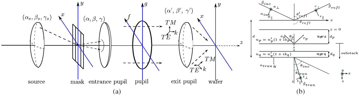
Fig. 1. (a) Schematic of forward lithography. (b) Reflection from and transmission through a stratified medium.
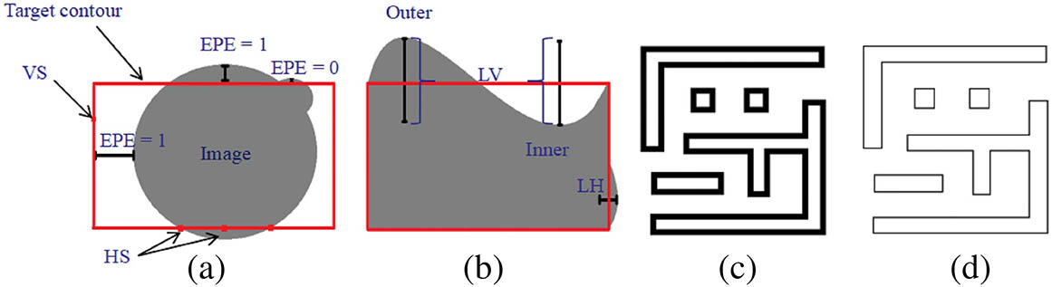
Fig. 2. (a) EPE measurement illustration. (b) Numerical superposition region. (c) Pattern edge set (PES). (d) Edges of target pattern 4(c) .
Fig. 3. PV Band demonstration. (a)–(c) Printed images under different process conditions. (d) Computed PV Band. (e) PV Band of the printed images with 4(c) illuminated by the annular source in Fig. 4(a) .
Fig. 4. (a) Annular source
Fig. 5. Printed wafer images with (a) PE 4494 and (d) PE 5193, EPE images with (b) EPE 1158 and (e) EPE 1512, PV Band images with (c) PV Band 2347 and (f) PV Band 3965 with respect to target patterns 4(a) .
Fig. 6. Simulation results with
Fig. 7. Randomly initialized masks within the range
Fig. 8. Simulation results with
Fig. 9. Convergence of (a) 8 , (c) 8(a) and 8(b) , and (d) 8(c) and 8(d) .
|
Table 1. Wafer Stack Parameters
| |||||||||||||||||||||||||||||
Table 2. Spe, Sepe, and Spv of the Simulations in Figs. 5 and 6
| ||||||||||||||||||||||||||||||||||
Table 3. Spe, Sepe, and Spv of the Simulations in Figs. 5 and 8

Set citation alerts for the article
Please enter your email address
© Copyright 2018-2021 | Chinese Laser Press. All Rights Reserved 沪ICP备15018463号-20