1School of Automation, Guangdong University of Technology, Mega Education Center South, Guangzhou 510006, China
2Guangxi Key Laboratory of Multimedia Communications and Network Technology, School of Computer, Electronics and Information, Guangxi University, Nanning 530004, China
We develop a source and mask co-optimization framework incorporating the minimization of edge placement error (EPE) and process variability band (PV Band) into the cost function to compensate simultaneously for the image distortion and the increasingly pronounced lithographic process conditions. Explicit differentiable functions of the EPE and the PV Band are presented, and adaptive gradient methods are applied to break symmetry to escape suboptimal local minima. Dependence on the initial mask conditions is also investigated. Simulation results demonstrate the efficacy of the proposed source and mask optimization approach in pattern fidelity improvement, process robustness enhancement, and almost unaffected performance with random initial masks.
Optical microlithography is increasingly challenging with the ever growing integration intensity of semiconductor devices in the sub-22-nm technology node and low regime. To this end, resolution enhancement techniques (RETs)[1,2] become essential for printing a good quality wafer image including modified illumination schemes, rule-based and model-based optical proximity correction (OPC)[3]. Moving beyond model-based OPC, the inverse lithography technique (ILT)[4,5] inverts the imaging model and attempts to directly synthesize the optimized mask pattern. With the development of pixelated sources[6], source and mask optimization (SMO) becomes an integral part of ILT to improve the imaging performance by expanding the solution space of the source and mask with the joint optimization of the illumination and mask shapes[7,8].
Various computational strategies including pixelated patterns[7–10], pupil and mask topology compensation[11], Zernike source representations[12], wave front modulation[13–15], and compressive sensing[16,17] are incorporated into the SMO framework, which is readily solved by gradient-based methods[18–21]. Special attentions have been paid to dose sensitivity[18], defocus[19], and dose-focus matrix[22]. However, process variability band (PV Band), one important criterion for measuring process manufacturability indicating the physical representation of the layout sensitivity to process variations, is too complicated to be explicitly incorporated into the cost functions. Similarly, edge placement error (EPE) which evaluates the printed image contour under nominal conditions, is often excluded because of lack of differentiable formulations.
Gao et al.[23] developed objective formulations of EPE and PV Band with a scalar lithographic imaging model. Practically, selections of the step size in gradient-based methods generally face the dilemma where too small step-size subjects slow convergence and too large step-size fluctuation is around the minimal or even divergence. Besides, for sparse source and mask patterns with very different feature frequencies, updating them to the same extent is not appropriate where large updates should be performed for rarely occurring features. Accordingly, adaptive gradient method such as AdaGrad performs smaller updates for frequently occurring features and large updates for infrequent ones, and adaptive moment estimation (Adam) computes adaptive learning rates by keeping exponentially decaying averages of past square gradients and momentum. Therefore stability and the ability to escape suboptimal minimals are duly detected in the updating process.
Sign up for Chinese Optics Letters TOC. Get the latest issue of Chinese Optics Letters delivered right to you!Sign up now
This Letter focuses on the application of adaptive gradient methods including Adam and AdaGrad to lithographic SMO, which simultaneously considers pattern design in terms of pattern error (PE), EPE, and process window. We present explicit formulations of differentiable functions for EPE and PV Band, whose closed-form gradients are subsequently developed with vector imaging formation. Source patterns, where usually more sparsity is observed, and mask patterns are updated with AdaGrad and Adam methods, respectively. We also investigate the stability of the optimization process and the ability to escape suboptimal local minima when random initial masks are applied. Simulations show that the proposed SMO approach improves pattern fidelity and the process window with enhanced stability and unaffected initial condition performance.
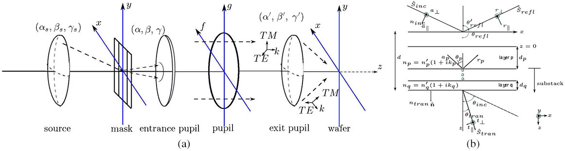
The wafer imaging process can be divided into two function blocks, namely the projection optics effects (coupling image formation) in Fig. 1 and resist effects. For a point source emanating a polarized electric field, the coupling image can be described as[3,20]where is an scalar matrix representing the source pattern distribution, is the sum of nonzero source intensities, are referred to as the equivalent filters, is the diffraction matrix to approximate the mask near-field, and means taking a pixel-wise square of amplitude. The resist effect can be approximated using a logarithmic sigmoid function with being the steepness of the sigmoid function and being the threshold. Therefore, the wafer imaging formation is described as .
Figure 1.(a) Schematic of forward lithography. (b) Reflection from and transmission through a stratified medium.
Given a target pattern , the goal of the SMO is to find the optimal source and mask pattern , which minimize the measured dissimilarity or “score ” between and , namely, in which the formula of in this work is defined as where , , and ensure pattern fidelity, minimize the EPE and the PV Band, respectively, and are weighted by predefined weight parameter . Parametric transformations and , with and , are applied to reduce the binary-constrained optimization problems to unconstrained ones in the updating procedure.
measures the sum of mismatches between and the desired one over all locations. For mathematical convenience, the square of the norm is frequently practiced in SMO, leading to the minimization of
The gradients of with respect to and are where is entry-by-entry multiplication, is the conjugate operation, rotates the matrix in the argument by in both the horizontal and vertical directions, is the convolution operation, is the all-ones matrix, and .
measures the geometrical distance of the image contour between and . However, lack of analytic formulation of a differentiable often complicates the explicit incorporation of EPE minimization. To this end, we formulate EPE as illustrated in Fig. 2(a) to include image difference in the horizontal and vertical inner image and outer image edges from sampled points on horizontal edges (HS) and vertical edges (VS). EPE violation is detected to be one when , with being a predefined threshold and zero otherwise. is computed for samples on vertical and horizontal edges within and , horizontal and vertical tolerable EPE segments depicted in Fig. 2(b). and are calculated according to the pattern edge set (PES) in Fig. 2(c) enwrapping the target pattern edge (TPE) in Fig. 2(d), under possible exposure latitude[1] describing tolerable target pattern linewidth. Subsequently, is calculated as where is the image difference between sampled points on HS with horizontal coordinate and points in with horizontal coordinate and vertical coordinate . With defined in Eq. (4), is similarly defined. is defined to be the summation of EPE violations (EPEVs) for all samples on HS and VS as
Figure 2.(a) EPE measurement illustration. (b) Numerical superposition region. (c) Pattern edge set (PES). (d) Edges of target pattern in Fig. 4(c).
For ’s differentiability, another sigmoid function is applied to , removing the binary-value constraints on EPE with being the steepness and being the threshold of . Consequently, the gradients of with respect to and are calculated as with or and in which is defined in Eqs. (5) and (6).
PV Band is a set of edges between the fix-printability areas (FPAs) and non-printability areas (NPAs) under possible process conditions, representing the robustness of process manufacturing. As illustrated in Fig. 3, the formulation of the PV Band in Fig. 3(d) requires a series of Boolean operations to extract the edge placement through all possible printed images from Figs. 3(a) to 3(c), which are extremely cumbersome and difficult to calculate. The red boxes present extracted edges of the target contact pattern, and the gray areas are the printed patterns with the extracted pattern edges in blue. in Eq. (3) is defined as where are printed images under process conditions, and are union and intersection operations, and the operation denotes the complement set of in . Noting ,
Figure 3.PV Band demonstration. (a)–(c) Printed images under different process conditions. (d) Computed PV Band. (e) PV Band of the printed images with in Fig. 4(c) illuminated by the annular source in Fig. 4(a).
Assuming the edge of the printed pattern is close enough to the desired printed pattern edge when is incorporated in the cost function and replacing with the target pattern , is reduced to the average of the summation of the norm of image differences to give with being the image difference under the process condition with defined in Eq. (3). Figure 3(e) shows the PV Band calculated using and . Therefore, the gradients of with respect to and can be routinely calculated according to Eqs. (4) and (5) as
Gradient-based searching such as steepest gradient descent (SGD) has been a preferred algorithm for the minimization of in Eq. (3). However, suffering from the sensitivity to step-size , SGD is often subject to running into unwanted local minimal with small and divergence if is too big. Moreover, the sparsity of or aggregates the dilemma of selection. Adam method combines the merits of AdaGrad and RMSPro methods, which works well with sparse gradients and naturally performs adaptive adjustments of . Therefore, in this Letter, AdaGrad and Adam methods are applied to updating the source and mask patterns or . In the Adam method, or at time-step is updated as where is the smoothing term to avoid division by zero, and and are the bias-corrected moment estimate of first moment and second moment , respectively, with , and , being the decay rates.
Assuming after initial optimization (IO) of which accumulates and , reaches a local minimum point at , where SGD cannot break symmetry, with and , at can be calculated as in which , and are regarded as the attenuation factors of , . It is therefore concluded that after the IO procedure of accumulating and , the attenuation factors gradually decrease and small enough to be close to zero, namely as the first-phase optimization (FPO).
Subsequently, we investigate the absolute value of at the end of (FPO) as where and are amplification factors with respect to and . With , , and close to 0, , taking the smoothing term into account: at , if is close to 0, and , the iteration will act similarly to the iteration at and similarly for the following iterations until deviates significantly from zero. We name the above procedure the second-phase optimization (SPO), at the end of which is big enough to drive the updating of out of the SPO entering IO to escape the local minimum point.
Numerical simulations are performed on a lithography imaging system with wavelength , , spatial resolution , , and being the steepness and the threshold of the sigmoid function. The system is initially illuminated by an annular source with and in Fig. 4(a), with target patterns , in Figs. 4(b) and 4(c). The ranges of process conditions including dose, defocus, and linewidth tolerance are , , and , respectively. is calculated according to the parameters of the wafer stack given in Table 1. The corresponding , EPE, and PV Band images when printing and on the wafer illuminated by are given in Figs. 5(a)–5(c) and Figs. 5(d)–5(f), respectively. Severe distortions are observed exhibiting and and 1512 with respect to and , respectively. Violations of linewidth tolerance are also detected with and 3965 in Figs. 5(c) and 5(f), which has to be compensated for by radical computational techniques. When updating or at time-step using the SGD method with where , the step-size is set as 0.3, which is repeatedly tested for convergence, and when the proposed approach is applied, in Eq. (15) and decay rates , are suggested to be 0.1 and 0.9, 0.999.
Figure 5.Printed wafer images with (a) PE 4494 and (d) PE 5193, EPE images with (b) EPE 1158 and (e) EPE 1512, PV Band images with (c) PV Band 2347 and (f) PV Band 3965 with respect to target patterns and illuminated by the annular source in Fig. 4(a).
In Fig. 6 where the proposed method and the SGD method are applied to the simulation, the columns represent the optimized source pattern , the optimized mask pattern , the EPE images, and the PV Band images simulated with the optimized illuminated by the optimized . Two weight parameters, and , are used that emphasize EPE and PV Band minimization, respectively. Figures 6(a)–6(d) show the simulation results with as the target pattern, using the proposed algorithm and the SGD method weighted by and , respectively. The values of , , and of the simulations in row of Fig. 5 and Figs. 6(a)–6(d) are recorded in Table 2. Significant improvements of PE, EPE, and PV Band are duly observed to reduce from 4494, from 1158, and from 2347 in Fig. 5(a)–5(c) to , , and in Figs. 6(a)–6(d) with target pattern .
Fig. 5
Fig. 6
row I01
(a)
(b)
(c)
(d)
Spe
4494
614
540
586
490
Sepe
1158
172
175
174
143
Spv
2347
2246
1834
2211
1885
Table 2. Spe, Sepe, and Spv of the Simulations in Figs. 5 and 6
Figure 6.Simulation results with as the target pattern. Columns from left to right: the synthesized source pattern , the synthesized mask pattern , the EPE images, and the PV Band images illuminating by . Rows: proposed approach (a) with and (b) with , SGD (c) with and (d) with .
The initial mask in the simulations in Fig. 6 is defined as an matrix with each element equaling , which proves feasible for both the proposed approach and the SGD method. However, the initialization value and step-size are time-consumingly decided through many experiments, which greatly increase the workload of the simulations. Alternatively, with random initial masks in Fig. 7, another set of simulations is performed in Fig. 8 with target pattern and weight parameter to show the impact of initial masks on the optimization process. The columns present , , the EPE images, and the PV Band images simulated with illuminated by . Two random initial masks and in Figs. 7(c) and 7(d) are, respectively, applied to Figs. 8(a) and 8(b), using the proposed approach, Figs. 8(c) and 8(d) using the SGD method with weight and target pattern . The values of , , and of the simulations in row of Fig. 5 and Figs. 8(a)–8(d) are recorded in Table 3, where stands for not available. It is observed that for initial random masks and , the proposed approach still reaches satisfactory local minimum, however, the SGD method starting with and finds it difficult to break symmetry to escape an unwanted local minimum resulting in poor OPC performance, showing great initial condition dependence of the SGD method.
Fig. 5
Fig. 8
Fig. 5
Fig. 8
row I01
(a)
(b)
row I02
(c)
(d)
Spe
4494
567
n.a.
5193
468
n.a.
Sepe
1158
178
n.a.
1512
96
n.a.
Spv
2347
1867
n.a.
3965
2472
n.a.
Table 3. Spe, Sepe, and Spv of the Simulations in Figs. 5 and 8
Figure 8.Simulation results with and as the target pattern and weight . Rows: (a) and (c) proposed approach with and , (b) and (d) SGD with and as initial masks.
The convergence of and in the simulations in Fig. 8 is drawn in Figs. 9(a) and 9(b). In Figs. 9(c) and 9(d), special inspections are taken to investigate the convergence of when initial masks and in Figs. 7(a) and 7(b) are, respectively, applied to Figs. 8(a) and 8(b), Figs. 8(c) and 8(d) with the proposed approach and the SGD method. In Figs. 9(c) and 9(d), with the SGD method, a small renders very small values of with random initial masks and and inhibits the update of to break symmetry when the optimization of hits the local minimum, presenting very poor convergence, while a bigger will lead to divergence in later iterations. On the contrary, the proposed algorithm uses bias-corrected first moment and second moment estimates , to constrain the gradients of the objective functions, and therefore, at a certain step when the updating process reaches a local minimum, IO accumulates the moments , and enters the FPO to attenuate , as small enough to be close to 0 to subsequently break symmetry by entering the SPO. Such supersedure of IO, FPO, and SPO in the updating of can be observed in the Figs. 9(c) and 9(d), showing the ability of the proposed approach to escape unwanted local minima when random initial masks are applied. It should also be mentioned that the simulations in Fig. 8 present similar results for and with weight , showing the generality of the proposed approach.
Figure 9.Convergence of (a) , (b) of the simulations in Fig. 8, (c) of the simulations in Figs. 8(a) and 8(b), and (d) of the simulations in Figs. 8(c) and 8(d).