Abstract
The impact of operation current on the degradation behavior of 310 nm UV LEDs is investigated over 1000 h of stress. It ranges from 50 to 300 mA and corresponds to current densities from 34 to . To separate the impact of current from that of temperature, the junction temperature is kept constant by adjusting the heat sink temperature. Higher current was found to strongly accelerate the optical power reduction during operation. A mathematical model for lifetime prediction is introduced. It indicates that lifetime is inversely proportional to the cube of the current density, suggesting the involvement of Auger recombination.1. INTRODUCTION
Al(In)GaN-based ultraviolet light-emitting diodes (UV LEDs) with emission wavelengths between 280 and 320 nm are promising candidates for a variety of applications such as UV curing [1], phototherapy [2], and plant growth lighting [3]. Currently, the lifetime of UVB LEDs is still far inferior to that of LEDs emitting in the UVA and blue spectral regions. To overcome this lifetime issue, understanding the various degradation processes taking place in the LED during operation is essential. These processes may be affected differently by stress parameters such as temperature and current, which potentially allows for their distinction.
In this work, the focus will be on the impact of current on degradation of 310 nm UV LEDs at fixed temperature. Besides gaining a deeper insight into the physics behind the current-induced degradation processes, the aim is to derive a mathematical model that enables lifetime prediction and accelerated device testing. To the best of our knowledge, such a model predicting the long-term current-dependent degradation of UVB LEDs is still missing in the literature.
For UVB LEDs, it was already shown that constant current operation reduces the optical power and that higher current densities lead to faster optical power degradation [4–6]. Also, for nitride-based visible LEDs, a current-driven degradation was found [7], but there are works indicating only a weak impact of the current compared to the temperature [8,9]. For example, the lifetime of white LEDs was found to be inversely proportional to the current with an exponent of 0.17 [9].
Sign up for Photonics Research TOC. Get the latest issue of Photonics Research delivered right to you!Sign up now
2. EXPERIMENTAL SETUP
The 310 nm UV LED heterostructures were grown on (0001) sapphire substrates using metalorganic vapor phase epitaxy (MOVPE). The structure consists of a 1700 nm thick AlN buffer layer followed by a 200 nm AlN/GaN short-period superlattice and a 500 nm undoped and a 4.5 μm silicon-doped contact layer. The active region comprises a threefold Al(In)GaN/Al(In)GaN quantum well (QW) for a 310 nm emission. The p side consists of a 15 nm thick graded (decreasing Al content in the growth direction) AlGaN:Mg electron blocking layer, a 150 nm AlGaN:Mg/AlGaN:Mg short-period superlattice, and a 20 nm GaN:Mg contact layer.
After epitaxial growth, the LEDs were fabricated using standard chip processing technologies. The p electrodes are based on platinum, while the n electrodes are based on vanadium and aluminum [10,11]. For better heat extraction, the LED chips were flip-chip mounted on AlN ceramic packages using AuSn solder. The package was left open, i.e., no encapsulation was applied. Subsequently, the packaged LEDs were soldered on printed circuit boards (PCBs) with an aluminum core, which were affixed to the heat sink with screws. A thermal resistance of about 24 K/W between the pn junction and the heat sink was determined experimentally and by simulations. At 100 mA, the typical optical power and operation voltage are about 6 mW and 9 V, respectively.
After mounting, four batches of 15 nominally identical LEDs were subjected to constant current operation for at least 1000 h. For each batch, the investigated samples were selected from various areas of the wafer. Thus, nonuniformities in epitaxial growth or the chip process across the wafer were taken into consideration for the evaluation. Each batch was operated at a different current (50, 100, 200, and 300 mA). The nominal stress current density is defined as the measured operation current divided by the p-contact area (). Hence, the stress current densities used hereafter are as shown in Table 1. However, possible local deviations of the effective current density in the active area from the nominal value are not taken into consideration. By means of additional pulsed measurements, a linear behavior of the optical power with respect to the current density was observed. Therefore, the investigated current densities are in a range where no current-density-induced efficiency droop is visible [12,13].
| Experiment | Current | Nom. Current Density | Heat Sink Temp. | Operation Time |
| No. | (mA) | (A/cm2) | (°C) | (h) |
| 1 | 50 | 33.5 | 75±1 | 4300 |
| 2 | 100 | 67.0 | 71±1 | 1000 |
| 3 | 200 | 134 | 41±1 | 1000 |
| 4 | 300 | 201 | 14±1 | 1000 |
Table 1. Experimental Conditions Applied to the Investigated 310 nm UV LEDs
Depending on the operation current, the junction temperature increases due to Joule heating, which usually accelerates degradation [4,5,14]. To investigate the impact of current independently from temperature, the junction temperature has to be kept constant for the various currents. Taking into account the thermal resistance between the junction and the heat sink, a constant junction temperature of was realized by adjusting the heatsink temperature for each current as listed in Table 1.
The voltage and the relative power of the emission were measured during operation. Optical power measurements were performed using SiC photodiodes with a cutoff wavelength of 375 nm. Thus, contributions of parasitic luminescence at longer wavelengths are not considered. In addition, the emission spectra of aged and unaged samples were measured at 100 mA and 25°C using an uncalibrated compact spectrometer. Stable temperatures throughout the operation were proved by tracking the temperatures of the PCBs.
3. RESULTS
The normalized emission spectra of an aged LED and an unaged LED are exemplarily shown in Fig. 1. The LEDs show single peak emission at a wavelength of about 310 nm. Both before and after aging, the intensity of the QW emission peak is about 2 orders of magnitude larger than the parasitic emission at longer wavelengths. Thus, the relative optical power measured during operation can be assigned to the QW emission. The intensity of the parasitic emission differs slightly from sample to sample and shows no clear trend that could be correlated to the operation conditions. Possible changes of the wavelength or of the half-width of the emission peak due to current stress are either nonexistent or too small to be detected.
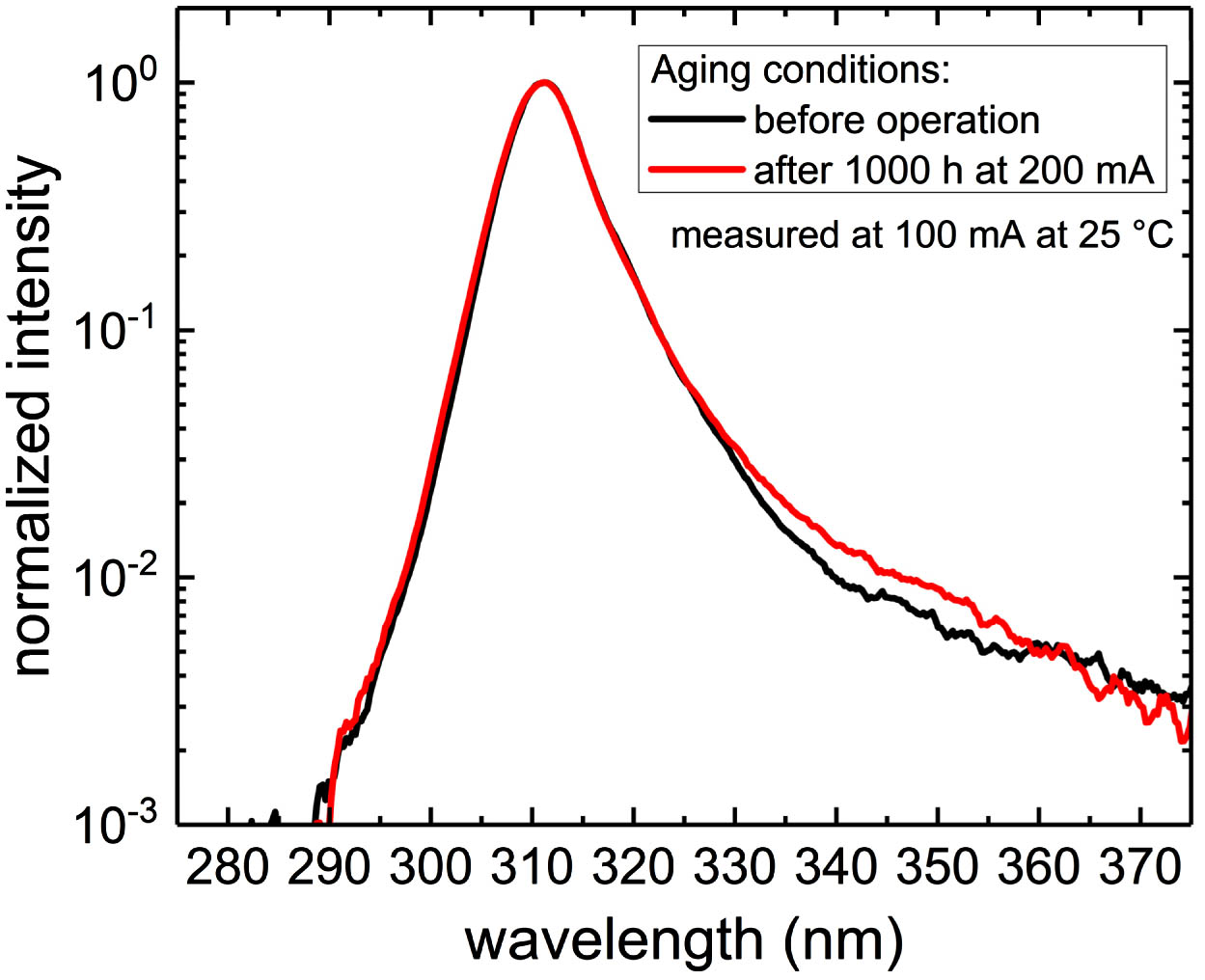
Figure 1.Representative emission spectra of the investigated 310 nm UV LEDs normalized to the emission peak. The spectra were measured at 100 mA at a heat sink temperature of 25°C before aging and after aging experiment 3 (Table 1).
The relative reduction of the optical power is shown in Fig. 2 for different operation current densities. The data points correspond to mean values obtained from 15 LEDs of each batch. The error bars correspond to the standard error of the mean. The experiment reveals that higher current densities result in a faster degradation. As already observed in other works [4,14,15], the optical power reduces faster at the beginning of operation, i.e., during operation the degradation slows down. This is the case for all current density levels in this investigation. Interestingly, at long operation times the degradation rate is almost independent of the current density.

Figure 2.Optical power over time of LEDs run at different current densities. The values are normalized to the initial value and averaged over 15 LEDs. For all currents, the junction temperature was kept at .
The lifetime , when the optical power has reduced to 70% of the initial value, was determined and plotted versus the current density (Fig. 3) to describe the dependency of the degradation on the current density analytically. The points and error bars result from averaging the values of 15 LEDs per current density. The lifetime of the investigated 310 nm UV LEDs is about 370 h at an elevated current density of about , which is comparable to values of 500–1000 h reported by others [16] for UVB LEDs operated at similar conditions. In the double logarithmic plot in Fig. 3, all data points follow a straight line, which can be described by Eq. (1) as follows: Here, is the current density and is a constant. The exponent is extracted from the slope of the curve in the double logarithmic plot. Therefore, the lifetime is inversely proportional to the cube of the current density, resulting in a considerable extension of lifetime by reducing the current density.
Figure 3.Operation time at which the optical power has reduced to 70% () of the initial value versus current density.
The functional dependency of Eq. (1) does not only hold for the specific power reduction to 70%. Figure 4 shows the relative reduction of the optical power plotted versus time multiplied with the cube of the current density. All points lie nearly perfectly on top of each other. Therefore, Eq. (1) generally holds up for all degradation levels between 100% and 50%, and the cube of the current density is a common scaling factor for the temporal progression of the optical power. The cubic dependency on the current density was also observed for various other 310 nm UV LEDs with different heterostructures.
Figure 4.Mean normalized optical power of the LEDs versus the product of the operation time and the cube of the current density.
Finally, the functional dependency of the optical power on the operation time will be examined more closely. For visible LEDs it is reported that the temporal reduction of the optical power follows an exponential function [17,18]. Furthermore, a square-root time dependency was observed for UVB LEDs [4]. However, the investigated 310 nm UV LEDs neither show an exponential nor a square-root time dependency. Logarithmic scaling of the time axis (Fig. 5) reveals that for all current densities the optical power follows a nearly perfect straight line for operation times longer than a characteristic time . Combining the logarithmic time dependency with the previously discussed impact of the current density results in Eq. (2), which describes those straight lines (dashed lines in Fig. 5), we have The parameters and are constants for all investigated current densities.
Figure 5.Mean normalized optical power (see Fig. 2) versus logarithmic time scale. For different current densities, the characteristic times are indicated. Also shown are the logarithmic functions (dashed lines) from Eq. (2) and the extended logarithmic function (solid line) from Eq. (4).
For short operation times, obviously Eq. (2) cannot properly describe the experimental data, as it exceeds 100%. Therefore, the characteristic time is introduced as the intersection of the logarithmic function [Eq. (2)] with the relative optical power of 100%. In Fig. 5 the characteristic times to are marked for the four different current densities. Using Eq. (2) with , one obtains Analogous to Eq. (1), the characteristic times are inversely proportional to the cube of the current density. A simple approach to describe the evolution of the optical power over the whole operation time, which meets the boundary condition , is to include the characteristic time as a time offset in Eq. (2) as follows: Figure 5 shows the fit (solid lines) of Eq. (4) to all the experimental data. The empirical function fits well to the data with deviations smaller than 4%.
4. DISCUSSION
The fact that degradation scales with the cube of the current density suggests that a process of three charged particles may be involved. In a first approximation, the density of carriers in the active region is proportional to the current density [19]. Since the Auger recombination rate is proportional to the cube of the carrier density in the active region, Auger recombination is suggested to be involved in the degradation. Auger recombination in group-III-nitride-based LEDs has already been studied extensively by other groups [12,20]. Assuming Eq. (1) results in where is the lifetime until a specific level of optical power degradation is reached. The related constant [compared to Eq. (1)] is proportional to , which can be interpreted as the number of Auger recombination events leading to a specific optical power reduction . A possible scenario is that, depending on the current density, Auger recombination during operation generates “hot” carriers (electrons and/or holes), i.e., carriers with high energy [12]. These carriers could activate pre-existing point defects or complexes in or around the active region that increase the Shockley–Read–Hall (SRH) recombination rate and/or trap-assisted tunneling conduction [4,5]. As a consequence, the optical power decreases. The activation of pre-existing point defects in thin-film GaN samples has already been investigated by Nykänen et al. using a low-energy electron beam [21]. The authors identified the activated defects as Ga vacancies and proposed that initially passive complexes are activated by H removal. In addition, Chichibu et al. studied nonradiative recombination centers (NRC) in and concluded that vacancy complexes such as and are the major NRCs [22]. It is possible that those complexes are initially passivated and are activated later by H removal. However, the suggested Auger recombination is not necessarily the only process contributing to the degradation of 310 nm UV LEDs. Rather, Auger recombination might be dominant for the degradation in the investigated sample structure, whereas other processes may dominate in other samples. It has to be considered that the rate could be strong enough to be responsible for long-term degradation, but can be too small to cause an efficiency droop.
It should be noted that the logarithmic time dependency of the optical power is in contrast to other works where a square-root time dependency was found and attributed to a diffusion process [4,23,24]. It can therefore be assumed that diffusion is most likely not the dominant process for the degradation of the investigated samples. To the best of our knowledge, a logarithmic time dependency has not yet been reported for the degradation of LEDs. However, it is typically observed for Si-based metal-oxide semiconductor field effect transistors (MOS-FETs) and attributed to an increase of trapped charge carriers [25–28]. This could be an indication that carrier trapping plays a role in the degradation of 310 nm UV LEDs. This idea would be consistent with the before-mentioned activation of pre-existing point defects.
Finally, the characteristic time when the logarithmic time dependency of the degradation starts needs to be discussed. One possible explanation for the existence of such a starting point is that activation and/or generation of point defects improves the carrier injection efficiency into the active region. This effect would increase the radiative recombination rate and therefore increase the optical power [29,30]. For example, the often-discussed breaking of Mg-H complexes [5,29–32] activates the magnesium acceptors and possibly enhances hole injection efficiency. If this process was superimposed on an increase of the SRH nonradiative recombination rate, both effects could cancel each other. After the characteristic time is passed, the improvement of carrier injection is possibly completed (for example, since most of the H has been removed and Mg acceptors are nearly fully activated), and the increase of the nonradiative recombination at point defects dominates the behavior of the optical power with time.
5. SUMMARY
It was found that the cube of the operation current density is a scaling factor for the time dependency of the optical power of 310 nm UV LEDs. This means that the current density strongly affects the lifetime of these devices. For example, halving the current density increases the lifetime by a factor of 8. Thus, an enlargement of the active (p-contact) area can be an effective strategy to improve reliability.
Furthermore, Auger recombination was suggested to be involved in the degradation. Consequently, an adjustment of the carrier distribution in the active region, e.g., by increasing the number of QWs, can be an approach to improve the lifetime.
Finally, a mathematical model was empirically derived that is based on a logarithmic dependency on time. It enables lifetime prediction as well as accelerated testing of 310 nm UV LEDs.
Acknowledgment
Acknowledgment. The authors thank Andreas Kaiser, Sylvia Hagedorn, Katrin Hilbrich, and Alina Traut for their contributions to the preparation of the samples.
References
[1] A. Endruweit, M. S. Johnson, A. C. Long. Curing of composite components by ultraviolet radiation: a review. Polym. Compos., 27, 119-128(2006).
[2] J. Krutmann, A. Morita. Mechanisms of ultraviolet (UV) B and UVA phototherapy. J. Invest. Dermatol. Symp. Proc., 4, 70-72(1999).
[3] M. Schreiner, J. Martınez-Abaigar, J. Glaab, M. Jensen. UV‐B induced secondary plant metabolites. Opt. Photonik, 9, 34-37(2014).
[4] J. Glaab, C. Ploch, R. Kelz, C. Stölmacker, M. Lapeyrade, N. Lobo Ploch, J. Rass, T. Kolbe, S. Einfeldt, F. Mehnke, C. Kuhn, T. Wernicke, M. Weyers, M. Kneissl. Degradation of (InAlGa)N-based UV-B light emitting diodes stressed by current and temperature. J. Appl. Phys., 118, 094504(2015).
[5] C. G. Moe, M. L. Reed, G. A. Garrett, A. V. Sampath, T. Alexander, H. Shen, M. Wraback, Y. Bilenko, M. Shatalov, J. Yang, W. Sun, J. Deng, R. Gaska. Current-induced degradation of high performance deep ultraviolet light emitting diodes. Appl. Phys. Lett., 96, 213512(2010).
[6] M. Meneghini, D. Barbisan, L. Rodighiero, G. Meneghesso, E. Zanoni. Analysis of the physical processes responsible for the degradation of deep-ultraviolet light emitting diodes. Appl. Phys. Lett., 97, 143506(2010).
[7] N. Narendran, Y. Gu, J. P. Freyssinier, H. Yu, L. Deng. Solid-state lighting: failure analysis of white LEDs. J. Cryst. Growth, 268, 449-456(2004).
[8] L. Liu, M. Ling, J. Yang, W. Xiong, W. Jia, G. Wang. Efficiency degradation behaviors of current/thermal co-stressed GaN-based blue light emitting diodes with vertical-structure. J. Appl. Phys., 111, 093110(2012).
[9] X. Yang, B. Sun, Z. Wang, C. Qian, Y. Ren, D. Yang, Q. Feng. An alternative lifetime model for white light emitting diodes under thermal-electrical stresses. Materials, 11, 817(2018).
[10] J. Rass, T. Kolbe, N. Lobo Ploch, T. Wernicke, F. Mehnke, Ch. Kuhn, J. Enslin, M. Guttmann, Ch. Reich, A. Mogilatenko, J. Glaab, Ch. Stölmacker, M. Lapeyrade, S. Einfeldt, M. Weyers, M. Kneissl. High-power UV-B LEDs with long lifetime. Proc. SPIE, 9363, 93631K(2015).
[11] M. Lapeyrade, A. Muhin, S. Einfeldt, U. Zeimer, A. Mogilatenko, M. Weyers, M. Kneissl. Electrical properties and microstructure of vanadium-based contacts on ICP plasma etched n-type AlGaN:Si and GaN:Si surfaces. Semicond. Sci. Technol., 28, 125015(2013).
[12] J. Iveland, L. Martinelli, J. Peretti, J. S. Speck, C. Weisbuch. Direct measurement of Auger electrons emitted from a semiconductor light-emitting diode under electrical injection: identification of the dominant mechanism for efficiency droop. Phys. Rev. Lett., 110, 177406(2013).
[13] W. Sun, M. Shatalov, J. Deng, X. Hu, J. Yang, A. Lunev, Y. Bilenko, M. Shur, R. Gaska. Efficiency droop in 245–247 nm AlGaN light-emitting diodes with continuous wave 2 mW output power. Appl. Phys. Lett., 96, 061102(2010).
[14] Z. Gong, M. Gaevski, V. Adivarahan, W. Sun, M. Shatalov, M. Asif Khan. Optical power degradation mechanisms in AlGaN-based 280 nm deep ultraviolet light-emitting diodes on sapphire. Appl. Phys. Lett., 88, 121106(2006).
[15] J. Ruschel, J. Glaab, M. Brendel, J. Rass, C. Stölmacker, N. Lobo-Ploch, T. Kolbe, T. Wernicke, F. Mehnke, J. Enslin, S. Einfeldt, M. Weyers, M. Kneissl. Localization of current-induced degradation effects in (InAlGa)N-based UV-B LEDs. J. Appl. Phys., 124, 084504(2018).
[16] A. Fujioka, K. Asada, H. Yamada, T. Ohtsuka, T. Ogawa, T. Kosugi, D. Kishikawa, T. Mukai. High-output-power 255/280/310 nm deep ultraviolet light-emitting diodes and their lifetime characteristics. Semicond. Sci. Technol., 29, 084005(2014).
[17] . Projecting Long Term Lumen Maintenance of LED Light Sources(2011).
[18] F. Wang, T. Chu. Lifetime predictions of LED-based light bars by accelerated degradation test. Microelectron. Reliab., 52, 1332-1336(2012).
[19] L. Wang, J. Jin, C. Mi, Z. Hao, Y. Luo, C. Sun, Y. Han, B. Xiong, J. Wang, H. Li. A review on experimental measurements for understanding efficiency droop in InGaN-based light-emitting diodes. Materials, 10, 1233(2017).
[20] E. Kioupakis, Q. Yan, D. Steiauf, C. G. Van de Walle. Temperature and carrier-density dependence of Auger and radiative recombination in nitride optoelectronic devices. New J. Phys., 15, 125006(2013).
[21] H. Nykänen, S. Suihkonen, L. Kilanski, M. Sopanen, F. Tuomisto. Low energy electron beam induced vacancy activation in GaN. Appl. Phys. Lett., 100, 122105(2012).
[22] S. F. Chichibu, A. Uedono, K. Kojima, H. Ikeda, K. Fujito, S. Takashima, M. Edo, K. Ueno, S. Ishibashi. The origins and properties of intrinsic nonradiative recombination centers in wide bandgap GaN and AlGaN. J. Appl. Phys., 123, 161413(2018).
[23] C. De Santi, M. Meneghini, G. Meneghesso, E. Zanoni. Degradation of InGaN laser diodes caused by temperature- and current-driven diffusion processes. Microelectron. Reliab., 64, 623-626(2016).
[24] K. Orita, M. Meneghini, H. Ohno, N. Trivellin, N. Ikedo, S. Takigawa, M. Yuri, T. Tanaka, E. Zanoni, G. Meneghesso. Analysis of diffusion-related gradual degradation of InGaN-based laser diodes. IEEE J. Quantum Electron., 48, 1169-1176(2012).
[25] R. da Silva, G. I. Wirth. Logarithmic behavior of the degradation dynamics of metal-oxide–semiconductor devices. J. Stat. Mech. Theory Exp., 2010, P04025(2010).
[26] M. Brox, A. Schwerin, Q. Wang, W. Weber. A model for the time- and bias-dependence of p-MOSFET degradation. IEEE Trans. Electron Devices, 41, 1184-1196(1994).
[27] Q. Wang, M. Brox, W. H. Krautschneider, W. Weber. Explanation and model for the logarithmic time dependence of p-MOSFET degradation. IEEE Electron Device Lett., 12, 218-220(1991).
[28] T. Grasser, B. Kaczer. Evidence that two tightly coupled mechanisms are responsible for negative bias temperature instability in oxynitride MOSFETs. IEEE Trans. Electron Devices, 56, 1056-1062(2009).
[29] J. Hu, L. Yang, L. Kim, M. W. Shin. The ageing mechanism of high-power InGaN/GaN light-emitting diodes under electrical stresses. Semicond. Sci. Technol., 22, 1249-1252(2007).
[30] F. Manyakhin, A. Kovalev, A. E. Yunovich. Aging mechanisms of InGaN/AlGaN/GaN light-emitting diodes operating at high currents. MRS Internet J. Nitride Semicond. Res., 3, e53(1998).
[31] A. Y. Polyakov, N. B. Smirnov, A. V. Govorkov. Enhanced tunneling in GaN/InGaN multi-quantum-well heterojunction diodes after short-term injection annealing. J. Appl. Phys., 91, 5203-5207(2002).
[32] S. M. Myers, A. F. Wright. Theoretical description of H behavior in GaN p-n junctions. J. Appl. Phys., 90, 5612-5622(2001).


