
Hong Guan, Hao Sun, Junlin Bao, Zhipeng Wang, Shuguang Zhou, Hongwei Zhu. High-performance RF Switch in 0.13 μm RF SOI process[J]. Journal of Semiconductors, 2019, 40(2): 022401
- Journal of Semiconductors
- Vol. 40, Issue 2, 022401 (2019)
Abstract
1. Introduction
RF front-end modules (FEMs) have become increasingly prominent with the increase in 4G and 5G mobile communication which is required for multi-band and multi-mode applications. The RF switch is the largest demand module in the RF FEM product; its performance directly determines the entire RF transceiver system. Insertion loss and isolation are two major parameters that measure the performance of the RF switch in addition to the linearity requirement (harmonics) and power handling capacity. However, achieving a trade-off among these various parameters is often difficult. Most previous studies on RF switch performance, such as those on insertion loss, isolation, and P0.1 dB, harmonics, are insufficient, since they do not consider the Ron × Coff metrics. Hence, this paper not only focuses on the optimization of the primary RF switch parameters, such as insertion loss, isolation, P0.1 dB, and linearity, but also measures the product Ron × Coff. A high-quality SPST RF switch is designed by improving switch structure and parameter optimization[
2. RF SOI process
The wireless communication industry has always been interested in integrating a multi-mode multi-band RF switch in one small and low-cost system. Undoubtedly, the RF SOI process is cost effective for RF switches in comparison to other technologies, such as conventional bulk CMOS, silicon-on-sapphire, and GaAs[
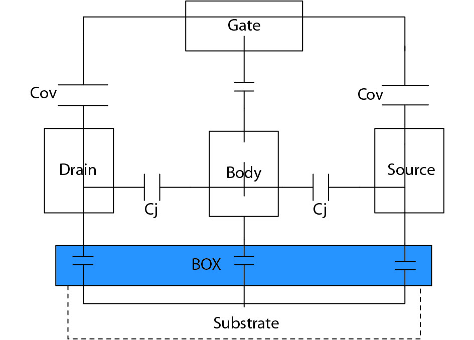
The low-Ron body-contact (BC) transistor is selected for the RF switch design as it can reduce insertion loss in the case of a large voltage swing and also has high voltage handling capability through device stacking, which can greatly increase linearity, while reduced Coff for improved isolation can also be achieved in the design. Fig. 1 shows inherently small overlap capacitance Cov and junction capacitance Cj of the transistor while the switch in the off state. Ron is measured from a single transistor; usually we measured Id @ 2.5 V Vg, 0.05 V Vd, then obtained Idin by normalizing Id to transistor width. In addition, we obtain Coff from Cov plus Cj, with Cov measured @ 0 V Vg, 45 mV 1 MHz AC condition, while Cj is measured @ 0 V Vb, 45 mV 1 MHz AC condition. Eqs. (1) and (2) give the transistor’s Ron and Coff measurement formulas and the figure of merit (FoM) of the RF switch can be obtained by using Eq. (3).
![]()
Figure 1.(Color online) Simplified capacitive models.
By ignoring the influence of other capacitances, only the effects of gate-to-source and gate-to-drain on overlap capacitance Cov are considered, because source-to-body, drain-to-body, and gate-to-body are too small for Cov,and junction capacitance Cj mainly refers to source-to-body and drain-to-body. As reducing Ron × Coff can improve the performance of linearity (P0.1 dB, harmonic), Ron reduction will be considered first[
The RF SOI Platform is much more preferable for the RF Switch module due to the excellent Ron × Coff performance; the ideal RF Switch should have much lower Ron in the turned-on state to transmit the RF signal with low insertion loss and high linearity. Furthermore, the RF switch should also have lower parasitic capacitance to block or isolate the unwanted RF signal in the turned-off state to maintain high terminal isolation. In most situations, Ron should be traded off against Coff, it is difficult to improve Ron while maintaining Coff at the same level and vice versa. Therefore, Ron × Coff is a good figure of merit by which to assess the RF SOI Platform performance.
3. Design optimization of RF switch
The most important parameters of the RF switch are insertion loss (IL), isolation (ISO), and power handling capacity measured by P0.1dB. Isolation and insertion loss are limited primarily by off-state parasitic capacitance and on-state current leakage. The IL and ISO can be expressed by Eqs. (4) and (5).
In commercial mobile phones, the GSM band transmit mode requires a power level at the antenna port as high as 35 dBm at 0.9 GHz and 33 dBm at 1.9 GHz and their maximum output power and maximum peak to peak voltage can be calculated as follows:
From Eqs. (6)–(8), 35 dBm power can be translated into 28.5 V peak voltage for a 4 : 1 VSWR, which requires stacked NFETs with breakdown voltage of 3.3 V in the GSM transmit paths to prevent transistors in the off-state from turning on, which greatly degrades signal linearity.
As shown in Fig. 2, we provide an improved series-shunt configuration by adding a big DC bias resistor and leakage preventing PFET in the schematic to optimize the overall performance of the RF switch. These stacked FETs are used to handle the GSM transmit mode high voltage swing and increase the power handling capability. The gate resistors (R1–R10) are used to improve the linearity of the RF switch while the body resistors are used to improve insertion loss by blocking the current leakage to the ground[
![]()
Figure 2.Proposed RF switch.
The optimized insertion loss and isolation of the RF switch should be balanced by selecting the best NFET transistor width. In Figs. 3(a) and 3(b), simulation results are given as the NFET width increases from 1.25 to 3.75 mm. Considering that large transistor width will increase parasitic capacitance and the reduction in insertion loss tends to be less, a 2.5 mm transistor width is selected. A typical value for the gate bias resistance is 50 kΩ. Fig. 4 shows a photomicrograph of the chip with a size of 0.4 × 0.5 mm2, including testing RF GSG pads.
![]()
Figure 3.(Color online) (a) Simulated IL for varying widths of NFETs at 0.9 and 1.9 GHz. (b) Simulated ISO for varying widths of NFETs at 0.9 and 1.9 GHz.
![]()
Figure 4.(Color online) Photomicrograph of RF switch chip.
4. Measurement and discussion
The designed RF switch chip is tested by using a network analyzer through the S-parameter for both insertion loss and isolation. The product of Ron and Coff is actually one of the key merits of the RF switch and a low FoM (120 fs) is given in Fig. 5.
![]()
Figure 5.Measured
Insertion loss and isolation are measured using an Agilent N9020A Network Analyzer, while P0.1 dB and harmonics are measured using an Agilent E4440A PSA Series Spectrum Analyzer. For insertion loss of this RF switch, the measurement bias voltages VB1 and V1 are 0, 2.5 V while VB2 and V2 are −2 V. As shown in Fig. 6, the RF switch exhibits low insertion loss of 0.24/0.34 dB and isolation (Fig. 7) takes on higher values of 28.8/22.4 dB at frequency bands of 0.9/1.9 GHz, respectively. The linearity of the RF switch is analyzed by P0.1 dB and harmonic measurements. The P0.1 dB(Fig. 8) is well beyond 36 dBm, meeting the GSM 900 standard, which dictates that the maximum available power at the antenna should be at least 33 dBm. The 2nd and 3rd harmonics were measured when a body is biased at 0 V and the gate is biased at 2.5 V. Fig. 9 shows another metric of linearity, the 2nd and 3rd order harmonics are lower than −41 at 34 dBm input power.
![]()
Figure 6.(Color online) Measured IL for RF switch.
![]()
Figure 7.(Color online) Measured ISO for RF switch.
![]()
Figure 8.(Color online) Measured
![]()
Figure 9.(Color online) Measured harmonics for RF switch.
Table 1 compares several key parameters with the relevant state-of-the-art RF switches reported. The performance of this SPST RF switch is comparable to that of the RF switch designed in HR SOI[
5. Conclusions
A high-performance RF switch with ultra-low insertion loss, high isolation, and linearity is achieved through 0.13 μm RF SOI. The inherent advantages of the SOI process combined with the optimization of the circuit structure significantly improve the performance of the RF switch. Results show a good performance for the SPST RF switch which is used in 4G and 5G mobile phone FEMs and can be used widely in forthcoming 5G technology.
Acknowledgements
This work was supported by the 111 Project (No. B12026).
References
[1] C L Chen, P W Wyatt, D R Yost. Fully depleted SOI RF switch with dynamic biasing. IEEE Radio Frequency Integrated Circuits Symposium, 175(2007).
[2] D Kelly, C Brindle, C Kemerling. The state-of-the-art of silicon-on-sapphire CMOS RF switches. Compound Semiconductor Integrated Circuit Symposium, 200(2005).
[3] S Makioka, Y Anda, K Miyatsuji. Super self-aligned GaAs RF switch IC with 0.25 dB extremely low insertion loss for mobile communication systems. IEEE Trans Electron Devices, 48, 1500(2001).
[4] F J Huang, O Kenneth. A 0.5-
[5] F Gianesello, A Momroy, V Vialla. Highly linear and sub 120 fs
[6] P A Rabbeni, A Joseph. RF SOI: revolutionizing RF system design. Microwave J, 58, 22(2015).
[7] X S Wang, X Wang, F Lu. Concurrent design analysis of high-linearity SP10T switch with 8.5 kV ESD protection. IEEE J Solid-State Circuit, 49, 1927(2014).
[8] X S Wang, X Wang, F Lu. A smartphone SP10T T/R switch in 180-nm SOI CMOS with 8kV + ESD protection by co-design. Custom Integrated Circuit Conference, 1(2013).
[9] B K Esfeh, M Rack, S Makovejev. A SPDT RF switch small and large signal characteristics on TR-HR SOI substrates. IEEE J Electron Devices Soc, 543(2018).
[10] C Tinella, O Richard, A Cathelin. 0.13
[11] I Song, M K Cho. PNP-based RF switches for the mitigation of single-event transients in a complementary SiGe BiCMOS platform. IEEE Trans Nucl Sci, 65, 391(2017).
[12] M D Wei, R Negra. High-isolation stacked RF switch using dc-lift and feed forward cancellation techniques in standard 65 nm CMOS. IEEE International Symposium, 1(2018).

Set citation alerts for the article
Please enter your email address
© Copyright 2018-2021 | Chinese Laser Press. All Rights Reserved 沪ICP备15018463号-20