
Ming Hui Fang, Yinong Xie, Fangqi Xue, Zhilin Wu, Jun Shi, Sheng Yu Yang, Yilin Liu, Zhihuang Liu, Hsin Chi Wang, Fajun Li, Qing Huo Liu, Jinfeng Zhu, "Optical colorimetric LiTaO3 wafers for high-precision lithography on frequency control of SAW devices," Photonics Res. 12, 341 (2024)
- Photonics Research
- Vol. 12, Issue 2, 341 (2024)
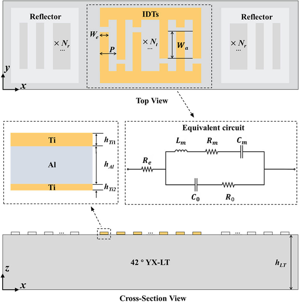
Fig. 1. Schematic drawing of the SAW resonator on the 42° YX-LT wafer, where W e N t N r
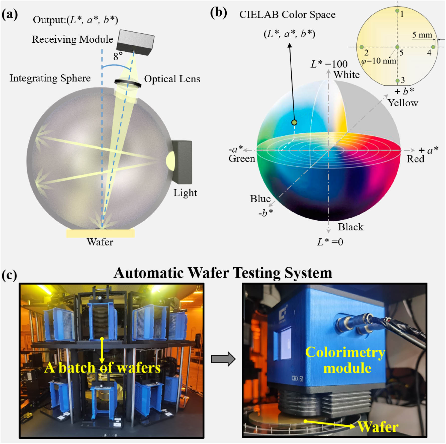
Fig. 2. Schematic drawing of the colorimetry scheme for LT-based wafers. (a) Optical measurement system. (b) CIELAB color space for the wafer evaluation, where the inset denotes measurement points on the wafer. (c) Photograph of the nondestructive colorimetry testing system for the LT-based wafer.
Fig. 3. Simulation of periodic models as a function of frequency and IDT width. (a) Frequency-dependent admittance curves for the 100 nm and 20 nm offsets of W e S / S max x – z
Fig. 4. Optical spectra of LT-based wafers with double-sided polishing. (a)–(c) LT wafers with various Fe doping densities. (d)–(f) Intrinsic and Fe-doped LT wafers and their partially reduced counterparts.
Fig. 5. Four-inch Fe:LT wafer and its corresponding reduced wafers with different reduction levels.
Fig. 6. (a) L * Δ E ab * L *
Fig. 7. (a) Schematic drawing of UV lithography for SAW resonators by using high - L * low - L *
Fig. 8. (a) SEM images of a fabricated SAW resonator for the Band 5 duplexer, where the SAW wavelength is 4.5 μm. (b) Simulated frequency-dependent admittance curves of the SAW resonators for two different IDT widths, which correspond to the measured counterparts for two different L * L * Δ E ab *
Fig. 9. Schematic drawing and photograph of bending strength test for wafers.


Set citation alerts for the article
Please enter your email address

© Copyright 2018-2021 | Chinese Laser Press. All Rights Reserved 沪ICP备15018463号-20