Ming Hui Fang, Yinong Xie, Fangqi Xue, Zhilin Wu, Jun Shi, Sheng Yu Yang, Yilin Liu, Zhihuang Liu, Hsin Chi Wang, Fajun Li, Qing Huo Liu, Jinfeng Zhu, "Optical colorimetric LiTaO3 wafers for high-precision lithography on frequency control of SAW devices," Photonics Res. 12, 341 (2024)
Copy Citation Text
【AIGC One Sentence Reading】:Our study introduces a colorimetry-based sensing method to enhance the lithography precision of SAW resonators made from LiTaO3 wafers, improving their frequency control in mobile communication filters.
【AIGC Short Abstract】:In this study, we introduced a novel method for enhancing the fabrication accuracy of Surface Acoustic Wave (SAW) resonators. By utilizing colorimetry to assess UV reflection in lithium tantalate (LiTaO3) wafers, we improved lithography precision and resonance frequency control. This innovative approach streamlines the manufacturing process and paves the way for advanced mobile communication device applications.
Note: This section is automatically generated by AI . The website and platform operators shall not be liable for any commercial or legal consequences arising from your use of AI generated content on this website. Please be aware of this.
Abstract
Surface acoustic wave (SAW) resonators based on lithium tantalate (LT, ) wafers are crucial elements of mobile communication filters. The use of intrinsic LT wafers typically brings about low fabrication accuracy of SAW resonators due to strong UV reflection in the lithography process. This hinders their resonance frequency control seriously in industrial manufacture. LT doping and chemical reduction could be applied to decrease the UV reflection of LT wafers for high lithographic precision. However, conventional methods fail to provide a fast and nondestructive approach to identify the UV performance of standard single-side polished LT wafers for high-precision frequency control. Here, we propose a convenient on-line sensing scheme based on the colorimetry of reduced Fe-doped LT wafers and build up an automatic testing system for industrial applications. The levels of Fe doping and chemical reduction are evaluated by the lightness and color difference of LT-based wafers. The correlation between the wafer visible colorimetry and UV reflection is established to refine the lithography process and specifically manipulate the frequency performance of SAW resonators. Our study provides a powerful tool for the fabrication control of SAW resonators and will inspire more applications on sophisticated devices of mobile communication.
1. INTRODUCTION
Surface acoustic wave (SAW) resonators are critical components of mobile communication filters [1–5]. In general, these filters are used to isolate diverse communication bands and avoid cross talk and unwanted noise signals, which puts demands on the high-precision frequency control of SAW resonators in industrial manufacturing [6–10]. For instance, the multiplexer of mobile communication is integrated by a series of SAW resonators, and the neighboring bands are very close in frequency (e.g., Bands 5, 8, 22, and 25); the excessive frequency offset of SAW resonance would lead to the generation of undesired signals between two adjacent bands [11]. Nowadays, lithium tantalate (LT, ) wafers are the most widely used acoustic-electric material for the fabrication of SAW resonators. The manufacture of LT-based SAW resonators is still hindered by the serious offset of the device resonance frequency. This is typically attributed to the large variety of surface metallization rates for interdigital transducers (IDTs) of SAW resonators [12–14], which is induced by multiple ultraviolet (UV) reflections in the intrinsic LT wafers that have high UV transparency [15,16].
In the past few years, researchers have tried to overcome the bottleneck of multiple UV reflections in intrinsic LT wafers, especially by using reduced and Fe-doped LT (Fe:LT) to tune the wafer optical properties for the fabrication of SAW resonators [17–20]. To test and control the quality and uniformity of reduced Fe:LT wafers, they usually measure a limited number of double-sided polished samples by conventional ultraviolet spectroscopy. Such a method not only brings about additional high costs but is also unfriendly to the following photolithography process for SAW resonators, in which single-sided polished wafers are required according to the IEC standards [21]. Up to now, the direct industrial measurement of reduced Fe:LT wafers with single-sided polishing has barely been reported. Therefore, a nondestructive measuring approach for on-line quality inspection of reduced Fe:LT wafers is still quite in demand for high-precision frequency control of SAW resonators in industrial manufacture.
Here, we propose a sensing scheme based on the wafer colorimetry of reduced Fe:LT with single-sided polishing, which is nondestructive to factory on-line inspection for high-precision frequency control of SAW resonators. In the study, we evaluated the optical spectra of reduced Fe:LT wafers to confirm the feasibility of our method. Unlike conventional destructive measurement, our work establishes the relationship between optical color properties and SAW resonance frequencies by a real-time approach. The research results demonstrate that wafer-scale colorimetry can precisely control the SAW resonance frequency through the accurate manufacture of IDT widths in the photolithography process. Our investigation can provide a powerful tool for significantly improving device performance and manufacturing yield of SAW resonators in mobile communication applications.
Sign up for Photonics Research TOC. Get the latest issue of Photonics Research delivered right to you!Sign up now
2. THEORY AND SIMULATION
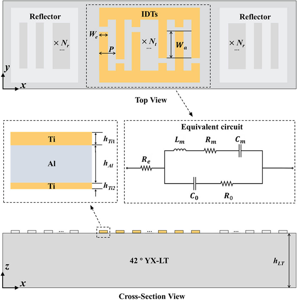
The typical SAW resonator structure is shown in Fig. 1. The resonator consists of an IDT with fingers located in the middle, and two grating reflectors with fingers on two sides to effectively reflect acoustic waves. It can be analyzed by the simplified equivalent circuit, where , , and denote the motional resistance, motional inductance, and motional capacitance, respectively; represents the resistance of the IDT, while provides a better description of acoustic loss when the circuit is in parallel resonance. is the static capacitance between the IDT and the LT-based wafer. Typically, the IDT width is designed as [22], and the SAW frequency is determined by , where and denote the SAW wavelength (4.5 μm) and velocity (3800 m/s), respectively. Thus, the SAW resonance frequency and anti-resonance frequency can be defined as below [23–25]:
Figure 1.Schematic drawing of the SAW resonator on the 42° YX-LT wafer, where is the width of the IDT, and and are 80 and 15, respectively.
With the aim to reveal the effects of IDT width on the device performance of the SAW resonator, we perform the piezoelectric simulation by the finite element method based on COMSOL Multiphysics [26]. The piezoelectricity-solid coupling module is adopted by neglecting any mechanical and electrical loss. The Euler angle of the LT-based wafer is (0°, , 0°). The IDT is the Ti/Al/Ti layer with the corresponding thicknesses of 0.03 μm, 0.16 μm, and 0.015 μm, respectively. Initially, we establish a three-dimensional periodic model to investigate the influence of IDT width deviation on resonance frequency offset and device stress distribution. In this model, the periodic boundary conditions are applied on the and directions, the period is 2 times the IDT width, and the thickness of the unit cell in the direction is taken as . Furthermore, we perform the simulation of a comprehensive device model in a two-dimensional form to validate the experimental results, where the IDT aperture size is 88 μm, and and are 80 and 15, respectively. Typically, the SAW can penetrate the LT-based wafer and propagate to a depth of , so the thickness of the wafer is set as . Additionally, the perfectly matched layer with thickness is used to absolutely reduce the wave reflection from the bottom boundary. The maximum length of meshing cells is as small as , which ensures the accuracy of numerical simulation.
3. FABRICATION, CHARACTERIZATION, AND MEASUREMENT
A. Fabrication and Characterization of SAW Resonators
The single crystals of LT are grown by the Czochralski method, and some of them are doped with Fe during their growing process. After crystal slicing, we obtain intrinsic and Fe-doped LT wafers, and some of them are treated with the reduction process. During the process, the wafers are coated with the carbonate powder mixed with a catalyst; then the deoxygenation is carried out using the mixture of and at temperatures over 390°C for 10 h [27]. After grinding, thinning, and chemical mechanical polishing, the single-sided polished wafers with the thickness of μ and flatness of μ are obtained (measured by Flatness Tester FT-900, NIDEK, Japan). All kinds of LT-based wafers are from Quanzhou San’an Integrated Circuit Co., Ltd. and prepared with the orientation of 42° YX cut. Based on the above processing methods, we prepare a variety of LT-based wafers, such as the LT, reduced LT (rLT), Fe:LT, and reduced Fe:LT (rFe:LT). The IDT of the SAW resonator is fabricated by the standard I-line lithography, metal deposition, and lift-off process on all the LT-based wafers [28–30]. To study the formation of IDTs on wafers, we adopt a test photomask with a periodically perforated slit width of 410 nm. The morphology of all fabricated SAW resonators is characterized by the scanning electron microscope (SEM, Carl Zeiss SIGMA HD, Germany). Their microscopic sizes are confirmed by the high-resolution SEM images. The influences of Fe doping and reduction on lithography accuracy are investigated. Ultimately, the SAW resonators for the Band 5 duplexer of mobile communication are fabricated and tested to evaluate our scheme.
B. Optical Measurement of Wafers
In order to confirm the wafer optical properties, the transmittance () and reflectance () ratios of LT, Fe:LT, and rFe:LT wafers with double-sided polishing are measured by a UV-vis spectrometer (Hitachi U-3900H). The corresponding absorbance () can be calculated according to the following Eq. (3) [31]:
The proposed nondestructive optical measurement for single-sided polished wafers is illustrated in Figs. 2(a) and 2(b). The testing system includes an LED white light source with 6500 K incident on a wafer sample via an integrating sphere. The light is diffusively reflected in the integrating sphere and monitored by a receiving module with an observation angle of 8°, which is based on the International Commission on Illumination (CIE) 15 standard. According to the CIELAB color space regulation of CIE 1976, a higher lightness value of represents a whiter wafer color, while a lower indicates a darker wafer color. The color difference among five wafer points can be expressed by the following Eq. (4): where and denote red/green and yellow/blue colors, respectively. , , and represent the maximum values of , , and , respectively; while , , and denote their minimum values. The locations of the five testing points are defined in the inset of Fig. 2(b). The automatic wafer testing system by the nondestructive colorimetry scheme is exhibited by the photograph in Fig. 2(c), while a multimedia file of the measuring procedures is provided in the Visualization 1.
Figure 2.Schematic drawing of the colorimetry scheme for LT-based wafers. (a) Optical measurement system. (b) CIELAB color space for the wafer evaluation, where the inset denotes measurement points on the wafer. (c) Photograph of the nondestructive colorimetry testing system for the LT-based wafer.
The electronic tensile testing system (ZCTL-W200N, Zhongchuang Testing Machine Co., Ltd., Jinan, China) is used to measure the bending strength of wafers. The measurement is based on the ISO 14704 test standard (see Appendix A for the details), as shown in Fig. 9. To ensure the validity and accuracy of the testing results, the wafers are placed in the same orientation, the wafer thicknesses are controlled within the variation range of μ, and is confined within a range of 1.5 to 2. The bending strength can be calculated according to the following Eq. (6): where is the downforce, is the distance between the two support rods, is the contact length, and is the wafer thickness.
4. RESULTS AND DISCUSSION
A. Influences of IDT Width on Device Performance by Theoretical Analysis
We first evaluate the influences of IDT widths on the resonance frequencies of SAW devices, as observed in Fig. 3. The frequency-dependent admittance curves for various periodic SAW device models are plotted in Fig. 4(a). They indicate that the smaller width offset of 20 nm can lead to the minimal offset of and with the standard deviation (SD) of () and (), respectively, whereas a larger width offset of 100 nm induces the much more significant frequency shift with the SD of 1.153 MHz () and (), respectively. The difference in frequency offset for two sets of IDT widths can be revealed by their normalized stress distributions. As shown in Fig. 3(b), the typical shear horizontal mode is stimulated, and the stress direction is along the axis [32–34]. Compared with the larger width offset of 100 nm, the smaller width offset of 20 nm hardly changes the stress distribution around , which can primely keep the resonance frequency feature of the device. According to this theoretical analysis, the control of IDT width should be a critical aspect of maintaining the high-precision frequency properties of SAW resonators.
Figure 3.Simulation of periodic models as a function of frequency and IDT width. (a) Frequency-dependent admittance curves for the 100 nm and 20 nm offsets of . (b) Normalized stress distributions () of the plane at the resonance frequencies of various SAW resonators.
Figure 4.Optical spectra of LT-based wafers with double-sided polishing. (a)–(c) LT wafers with various Fe doping densities. (d)–(f) Intrinsic and Fe-doped LT wafers and their partially reduced counterparts.
Since the IDT width is a crucial factor in the frequency response of a SAW resonator, we next focus on tuning the UV optical properties of LT wafers to precisely control the IDT width. In the beginning, our purpose was to lower the transparency of LT-based wafers for reducing multiple reflections during the lithography process with the 365 nm UV irradiation. Meanwhile, the basic mechanical and acoustic-electric properties of LT-based wafers should be maintained to ensure the device performance of SAW resonators. In order to tune the optical properties of LT wafers, we adopt two approaches, namely Fe-doping and reduction.
Beforehand, we investigated the UV-visible properties of Fe-doped LT wafers with double-sided polishing from Figs. 4(a)–4(c). Here we tune the Fe ion ratios from 0 ppm to 110 ppm (ppm, parts per million) in the low-degree doping range. It is observed that the Fe-doping wafers have much higher absorption in the UV range than that in the visible range. Particularly, the transparency at for the wafer of 110 ppm Fe doping is obviously decreased from 72.36% to 47.67%, while it has the highest absorbance of 49.69% and lowest reflectance of 2.64%. This implies that Fe doping should be an effective approach to lower the UV transparency of wafers. One should keep the main mechanical and acoustic-electric properties for LT-based SAW resonators, so the Fe doping should be confined at a relatively low level. The ratio of 110 ppm is typically applied, due to the necessity of consistent composition and a stable Curie temperature in LT [35,36], and we also use this Fe doping level for the next investigation.
We next investigate the effects of partial chemical reduction on intrinsic and Fe-doped LT wafers. Compared to the counterparts without reduction, the reductive wafers demonstrate a significant change in UV-visible properties, namely the more dramatical rise of UV and visible light absorbance, as observed in Figs. 4(d)–4(f). We find that the influences of partial reduction on the UV-visible spectra are greater than those of Fe doping. Particularly, the reduction treatment can largely increase the UV absorption at the wavelength of 365 nm. In combination with the effects of Fe doping and reduction, we can obtain the highest absorbance of 86.43% and decrease the reflectance to 0.82% at the wavelength of 365 nm, as illustrated in Figs. 4(e) and 4(f). Therefore, the Fe:LT wafers with partial reduction indicate great potential in the next UV lithography process [37,38]. We focus on the study of rFe:LT wafers with various reduction conditions in the next discussion.
C. Colorimetry Sensing of Reduced Wafers
During the on-line inspection, one prefers a nondestructive optical measurement on single-side polished wafers instead of double-side polished wafers. We exhibit a series of single-side polished wafers of rFe:LT with various levels of chemical reduction in Fig. 5. The lightness of these wafers is gradually lowered from light yellow to dark brown, as the level of reduction rises.
Figure 5.Four-inch Fe:LT wafer and its corresponding reduced wafers with different reduction levels.
Conventionally, such lightness differences are utilized to identify and classify LT-based wafers of various reduction conditions by the universal visual observation in person, which severely depends on the experiences of operators. The traditional approach would induce large batch-to-batch variations easily and hinder the high-throughput manufacture of wafers. The nondestructive lightness measurement based on the definite value of is a fast and effective way to evaluate the reduction levels of wafers. As shown in Fig. 6(a), the reduction level reflected by the value can be determined by the catalyst ratio and reaction temperature. The lightness is gradually reduced as the values of these two factors increase.
Figure 6.(a) and (b) as functions of the catalyst ratio and reaction temperature for rFe:LT wafers. (c) Transmittance, (d) absorbance, and (e) reflectance at the wavelength of 365 nm as functions of for rLT and rFe:LT wafers. (f) Wafer bending strength for various LT-based wafers. All the rFe:LT wafers have a Fe ion density of 110 ppm.
During the reduction process, in the wafer is reduced to , and the related reactions can be expressed as below [17]:
Initially, the lithium carbonate is heated to decompose into and . Under the high temperature and hydrogen atmosphere, further reacts to generate CO and . After that, the reductant CO induces the valence change from to . As more ions are changed to ions, the wafer becomes darker along with a smaller value. Particularly, more catalyst in lithium carbonate with a higher temperature enables more production of to accelerate the reduction reaction. The decrease of in Fig. 6(a) implies that the catalyst addition and temperature control have significant effects on changing the lightness of wafers. Contrary to Fig. 6(a), the color difference of a wafer is typically not influenced by the catalyst ratio and reaction temperature, as shown in Fig. 6(b). Actually, is mainly influenced by the uniformity of gas flow and thermal field in the reaction furnace.
We next utilize the colorimetry features of wafers and establish the relationship between and the UV response at the wavelength of 365 nm, as demonstrated in Figs. 6(c)–6(e). The visible values are measured on the single-side polished wafers, while the UV transmittance, absorbance, and reflectance are obtained after the corresponding wafers are double-side polished. The values of rFe:LT wafers have parameters greater than 0.91, which is much higher than those for rLT wafers. This indicates that the visible lightness values of rFe:LT can be more tightly correlated to the UV responses at the wavelength of 365 nm. It is also observed that the Fe-doped LT wafers exhibit significantly lower transmittance and reflectance along with higher absorbance for the same value. These results are consistent with the data for double-side polished wafers in Fig. 4 and imply that the colorimetry-based wafer measurement can be adopted as a nondestructive tool for the on-line test of single-side polished rFe:LT wafers.
Additionally, since the reduction and doping treatments might influence their mechanical properties [17], we continue to evaluate the bending strength of reduced and doped wafers in Fig. 6(f) aiming to maintain their robustness in manufacture. Typically, the bending strength of intrinsic LT wafers is around 225 MPa. As they are reduced to a low value of , the strength is decreased to about 200 MPa. One could perform a further chemical reduction with a lower value of for the low UV reflectance, as observed from Fig. 6(e); nevertheless, the further chemical reduction is decreased to 169 MPa on average. During the reduction process, the removal of oxygen atoms creates LT crystal structure vacancies and lowers the wafer’s mechanical strength. The strength value drops as more oxygen atoms are removed. In order to keep a high strength value, one could introduce the doping of Fe ions as shown in Fig. 6(f). Compared with the rLT wafers, the rFe:LT wafers have a higher bending strength up to 196 MPa. Therefore, we combine the procedures of doping and reduction to tune the optical properties and maintain mechanical stability.
D. Frequency Control of SAW Resonators
In the device structure of a SAW resonator, the IDT width is a critical parameter to determine the resonance and anti-resonance frequencies, according to Eqs. (1) and (2). The width of the IDT is influenced by the UV lithography process, where the UV absorption of LT-based wafers at the wavelength of 365 nm plays a key role, as shown in Fig. 7(a). We next investigate the effects of UV light going through the lithography mask, photoresist, and LT wafer. Compared with the wafer, the wafer supports higher UV absorption and lower reflection, which leads to a smaller area of UV light exposure on the photoresist. This results in a smaller width of IDT, which is closer to the size of the lithography mask pattern. We evaluate the width of the IDT as a function of for rFe:LT wafers in Fig. 7(b). The large value of 0.906 indicates the high correlation between the IDT width and wafer lightness. A larger value corresponds to a bigger IDT width, as demonstrated in Fig. 7(a). The fabricated IDT widths can be confined within a very small range from 407 to 413 nm by controlling values between 48 and 52. Therefore, the colorimetry of rFe:LT wafers can facilitate the high-precision control of IDT width for SAW resonators. In fabrication practice, the minimum size of is also limited by the pattern size of the lithography mask and the minimum value that can be achieved. In fact, the value cannot be too low and should be optimized since the high reduction level would degrade the mechanical and piezoelectric properties of LT wafers. In addition, we investigate the nonuniformity of IDT width as a function of on-wafer color difference, as shown in Fig. 7(c). The on-wafer nonuniformity of IDT width is elevated as the color difference becomes larger. In view of this, it is important to keep the on-wafer color homogeneity for highly uniform device fabrication. The above results demonstrate that and can be assumed as the crucial colorimetry parameters to evaluate and improve the fabrication quality of SAW resonators. The nonuniformity can be defined as below: where , , and are the maximum IDT width, minimum IDT width, and average IDT width, respectively. To further investigate the colorimetry sensing scheme, we fabricate the SAW resonators by the rFe:LT wafers with two different values and compare their frequency responses for the next discussion. We exhibit the SEM images of one representative SAW resonator for the Band 5 duplexer in Fig. 8(a). They show the good uniformity of IDT width and reflect the important geometry sizes of the fabricated device. We further analyze the frequency-dependent responses of the fabricated devices in Fig. 8(b). According to the full model simulation of SAW resonators, as the IDT width changes from 1225 to 1250 nm, both and have the same shift of 0.25 MHz toward the lower frequency band. Meanwhile, the measured frequency offsets of and for the corresponding values of 51.9 and 53.9 are both 0.25 MHz. The measurement and simulation results demonstrate the different frequency locations of and on the entire band, which might be due to a certain degree of deviation on the material parameters. Despite this, the measured frequency shift due to the change of value is consistent with the simulated frequency shift due to the change of IDT width. This indicates that one can precisely control the frequency response of a SAW resonator by tuning the lightness of the wafer. Furthermore, we compare the statistical and of all SAW resonators based on the two wafers with and in Fig. 8(c). Particularly, the dispersive and counts show the small SD values, which can be as low as 0.21 MHz. Figure 8(c) also illuminates that the on-wafer averaged and are 883.37 MHz and 915 MHz for , respectively; while the corresponding frequencies for are 883.74 MHz and 917.67 MHz, respectively. This data denotes that a higher value corresponds to the smaller averaged resonance and anti-resonance frequencies for all the devices on an rFe:LT wafer and one can also control their averaged performance by tuning its lightness values through manipulating the catalyst ratio and reduction temperature. Finally, we can assess the on-wafer device uniformity of resonance and anti-resonance frequencies by comparing the index of different wafers, as shown in Fig. 8(d). It demonstrates that a smaller of 1.63 has a much more uniform distribution of device resonance and anti-resonance frequencies than a larger of 3.15. Thus, the on-wafer color difference parameter can be adopted for the efficiency management of rFe:LT wafers, which also advances the on-line high-precision frequency control of SAW resonators during the wafer-based manufacture.
Figure 7.(a) Schematic drawing of UV lithography for SAW resonators by using and rFe:LT wafers. (b) IDT width as a function of rFe:LT wafer lightness. (c) Nonuniformity of IDT width as a function of rFe:LT on-wafer color difference.
Figure 8.(a) SEM images of a fabricated SAW resonator for the Band 5 duplexer, where the SAW wavelength is 4.5 μm. (b) Simulated frequency-dependent admittance curves of the SAW resonators for two different IDT widths, which correspond to the measured counterparts for two different values. (c) Device resonance and anti-resonance frequency distributions for the rFe:LT wafers with two different values. (d) On-wafer resonance and anti-resonance frequency distribution mappings for the rFe:LT wafers with two different values.
In summary, we propose a nondestructive color sensing method for the rapid measurement and testing of single-side polished wafers based on the reduced Fe-doped LT material. The effects of doping and reduction on the UV-visible properties of wafers are analyzed by the lightness and color difference. The study shows that the tuning of lightness allows for the high-precision control of SAW resonance and anti-resonance frequencies, and the on-wafer color difference provides a detection index for the standard confinement of device uniformity. Our research establishes a powerful tool for the mass production of SAW resonators, which will greatly promote their manufacturing quality and efficiency for applications on mobile communication.
Acknowledgment
Acknowledgment. The authors deeply appreciate Osamu Kawachi, of Sanan Japan Technology Co. (SJT), and Chih Pang Ma, of Quanzhou San’an Integrated Circuit Co., Ltd., for their advice and support.
APPENDIX A: BENDING STRENGTH TEST CONFIGURATION FOR LT-BASED WAFERS
The bending strength measurement method follows the ISO 14704 standard, as illustrated in Fig. 9. During the measurement, the wafer is positioned on top of two support rods, and then the loading rod is lowered and pressed until the wafer fractures. Measurement data are recorded using a load sensor and processed to determine the bending strength.
[7] S. B. Zhang, J. B. Wu, L. P. Zhang. Recent advances of radio frequency acoustic wave filters based on piezoelectric heterogeneous substrates. Navig. Control, 21, 29-39(2022).
[35] K. Masato, S. Ietaka, S. Takeharu. Single crystal for piezoelectric substrate, elastic surface wave filter using it, and manufacturing method thereof. Patent(2008).
 AI Video Guide
  AI Picture Guide
 AI One Sentence