
Mussaab I. Niass, Muhammad Nawaz Sharif, Yifu Wang, Zhengqian Lu, Xue Chen, Yipu Qu, Zhongqiu Du, Fang Wang, Yuhuai Liu. A contrivance of 277 nm DUV LD with B0.313Ga0.687N/B0.40Ga0.60N QWs and AlxGa1–xN heterojunction grown on AlN substrate[J]. Journal of Semiconductors, 2019, 40(12): 122802
- Journal of Semiconductors
- Vol. 40, Issue 12, 122802 (2019)
Abstract
1. Introduction
Vast promising applications for deep ultraviolet laser diode (DUVLD) in many fields such as wireless communication, medical instruments and chemical devices are still waiting for the higher performance of laser diode (LD) to be achieved[
Many studies have shown and demonstrated that the potential for exploiting h-BN in far-ultraviolet (FUV) emitters are due to its good characteristics[
2. Simulation model
The simulated laser diode structure was conducted via using LASTIP-Crosslight simulator software with a self-consistency model for varies quantity calculations. Were mirror reflectivity factors of (0.05) for both facets were assumed and a cavity length of 1500 µm. The spacer-1 and spacer-2 layers in the Table 1 were proposed for reducing the band-offset between AlGaN and BGaN layers.
3. Results and discussions
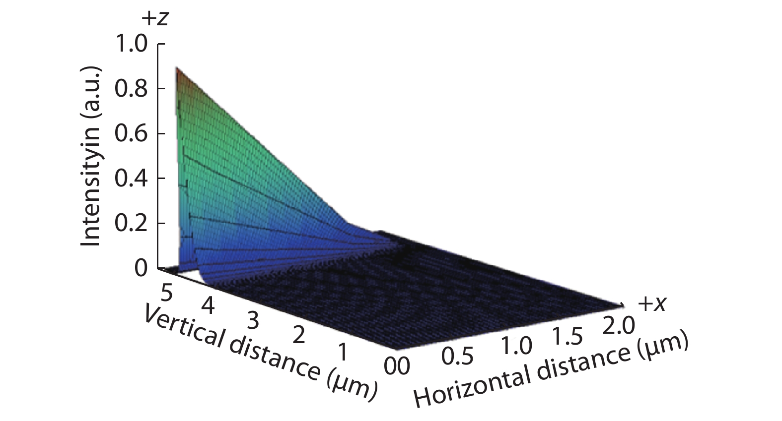
According to simulation results, it has been found that the minimum doping concentration that exhibits lasing at 277 nm for the given structure is NA= 5 × 1017 cm–3, ND= 9 × 1016 cm–3 with an OCF of 40.4 % as shown in Fig. 1. Therefore, different EBL design has been studied, firstly the conventional EBL contrivance which have a constant composition along the layer thickness assumed to be 10 nm, as well as an aluminum content of 80% (Al0.8GaN), were adjusted.
![]()
Figure 1.(Color online) The optical intensity confined within the active region for optical confining factor (OCF) of 40.4%.
Therefore, barely the structure produces an emission for Pmax= 115 µW given at a maximum current injection of Im= 550 mA and Ith = 150 mA as shown in Fig. 2. Whereas the V–I characteristic curve shows a semi-linear relationship for an approximated (biasing voltage) Vth = 7 V, with a DC resistance of 0.77 Ω.
![]()
Figure 2.(Color online) Illustrate the
Secondly, for the tapered (linearly graded) EBL contrivance a composition of Al0.65–0.80GaN was adjusted. Thus, the following quantities had been calculated by the simulator, were Pmax = 1.73 W at Imax= 1.65 A observed in Fig. 2 as well as Ith = 600 mA, S.E. = 1.468 W/A, Vth = 5 V, R = 0.239 Ω.
Thirdly, when a removal of EBL layer was established it shows an enhances in S.E. and threshold current almost by 15.8% and 8.3% achieved respectively, comparing to tapered design. Hence Pmax= 2.02 W at Imax = 1.65 A, Ith = 550 mA and S.E. = 1.70 W/A. On the other side, V–I curve shows a biasing voltage Vth = 5 V, R = 0.262 Ω, the lowest resistance is obvious since there is no EBL layer. Lastly, for an inverse tapered EBL contrivance as shown in Table 1 and in Fig. 3. gives Pmax = 2.4 W, Imax= 1.65 A, Ith = 500 mA and S.E. = 1.91 W/A a very good enhances were achieved in S.E. and Ith by 12.3% and 9% respectively, in addition to same tapered design threshold voltage was observed but different resistance of 0.336 Ω. Therefore, these results in well agree with published results at Ref. [12] in term of a better performance could be obtained, if tapered EBL design is applied instead of conventional EBL. Therefore this paper demonstrated an alternative opportunity of having higher performance for LD by using inverse tapered EBL design over tapered and conventional EBL.
![]()
Figure 3.(Color online) Schematic illustrations for the right half of simulated structure, real cavity length are 1500
Since the conventional EBL structure exhibits a very low emission power compared to other designs, probably due to low doping concentrations. Hence, we applied an increase in the doping concentration magnitude order, thus it had been found that an increase in NA and ND by two orders of magnitude up to NA = 5 × 1020 cm–3, ND = 9 × 1019 cm–3 lead to a clear stimulated emission in the conventional structure. Therefore, the simulated results for those concentrations shows same L–I and V–I characteristic curves for tapered, inverse tapered and without EBL designs, were Pmax = 103.8 W at Imax = 51.5 A, Ith = 500 mA, S.E. = 2.0 W/A, Vth = 4.6 V and R = 0.144 Ω as shown in Figs. 4(a) and 4(b). While the conventional structure shows enhance in the S.E. (3.14 W/A) by 57% compared to the other three designs in this high accepter and donor concentrations. Were Pmax = 50 W at Imax = 15.9 A, Ith = 130 mA Vth = 4.8 V, although a very good enhancement in S.E. is shown by the conventional design a higher resistance of 0.563 Ω compared to previously mentioned resistance for the other structures. In addition to a limitation in the maximum emitted power by almost 51% is observed, these limitations probably due to: (1) The electron leakage into the p-cladding layers, as shown in Fig. 5. (2) The band-offset height that forms as a result of EBL composition difference between the QB/Spacer-2, directly coupled to the resistance.
![]()
Figure 4.(Color online) Showing the (a)
![]()
Figure 5.(Color online) Showing the relationship between the averages calculated electron concentrations within the P-Cladding layer for different accepter and donor concentrations for the four EBL designs.
It has been found that the electron concentrations within the quantum well for the three designs (tapered, inverse tapered and without EBL) almost 1019–1020 cm–3. While the conventional EBL contrivance found to be 1018–1019 cm–3 which means lower concentration by one order of magnitude from the sufficient concentrations, therefore it is the probable reason for why there is no an apparent stimulated emission for the conventional structure, shown in Fig. 2 especially for lower accepter and donor concentrations.
For more elaboration of the first reason regarding the leakage of current/electrons, an analysis for the electron concentration in the p-cladding layer is summarized for the four different doping concentrations as shown in Fig. 5. Thus, it found that for a concentration of NA= 5 × 1017 cm–3, ND= 9 × 1016cm–3 the three designed structures show a low concentration of 1010 cm–3. While a larger amount of leakage current found for the conventional design ~ 1019 cm–3 almost similar quantity of electrons found in QW, that may mean there is no blocking happened for the electrons as could be observed from Fig. 6. This larger amount of leakage electron it has been evident to be due to insufficient EBL barrier/offset. While an attempt to increase the EBL composition for the given NA and ND concentrations seems to increase the Vth.
![]()
Figure 6.(Color online) Vertical cut view for the LD structure that illustrates the band diagram for the active region and EBL layer, with the
In addition to that, it will lead to a reverse increase of EBL height in the valence band, thus forming an undesired hole blocking layer that may directly degrade the p-type conductivity. On the other side, a tendency to increase the doping concentrations around 1019 cm–3 gives p-cladding layer concentration approximately to 1017 cm–3 for the three structures and 1011 cm–3 for a conventional design. These higher theoretical NA and ND i.e. > 10 18 cm–3 it might be difficult to implements practically, while NA and ND < 10 17 cm–3 have a higher possibility to be implemented for the demonstrated aluminum content.
4. Conclusion
The contrivances of a new combination between BGaN and AlGaN alloys were proposed, for B0.313GaN/B0.4GaN quantum well/quantum barrier assumed to be grown over AlN substrate. Hence a lasing in a deep ultraviolet range in 277 nm were observed, with a maximum emitted power of 2.4 W at an injection current of 1.65 A, threshold current of 500 mA and slope efficiency of 1.91 W/A that represents 9 %, 12.3% enhancement compared to tapered design respectively. With the lowest reported accepter and donor concentration for DUV devices of NA = 5 × 1017 cm–3, ND = 9 × 1016 cm–3.
In addition to an investigation regarding different EBL designs were shown. Therefore, we found it agreed well with the published results, moreover this paper proposes a probable better EBL design, especially for low doping concentrations, called inverse tapered EBL.
Acknowledgement
This work is provisioned by National Key Research and Development Program (Nos. NKRDP 2016YFE0118400), the Key project of Science and Technology of Henan Province (No. 172102410062), National Natural Science Foundation of China (No. 61176008), and National Natural Science Foundation of China Henan Provincial Joint Fund Key Project (No. U1604263).
References
[1] D B Li, n X J Sun, o C L Guo. AlGaN photonics: recent advances in materials and ultraviolet devices. Adv Opt Photon, 10, 43(2018).
[2] M Z Chowdhury, n M T Hossan, m A Islam et al. A comparative survey of optical wireless technologies: architectures and applications. IEEE Access, 6, 9819(2018).
[3] J R Chen, o T S Ko, u P Y Su et al. Numerical study on optimization of active layer structures for GaN/AlGaN multiple-quantum-well laser diodes. J Lightwave Technol, 26, 3155(2008).
[4] T Watanabe, a T Niiyama, a K Miya et al. Far-ultraviolet plane-emission handheld device based on hexagonal boron nitride. Nat Photonics, 3, 591(2009).
[5] K Watanabe, i T Taniguchi. Hexagonal boron nitride as a new ultraviolet luminescent material and its application. Int J Appl Ceram Technol, 8, 977(2011).
[6] H Kawanishi, a M Haruyama, i T Shirai et al. (BAlGa)N quaternary system and epitaxial growth on (0001) 6H-SiC substrate by low-pressure MO-VPE. Proc SPIE, 2994, 52(1997).
[7] M Kurimoto, o T Takano, o J Yamamoto et al. Growth of BGaN/AlGaN multi-quantum-well structure by metalorganic vapor phase epitaxy. J Cryst Growth, 221, 378(2000).
[8] T Honda, o M Kurimoto, M Shibata et al. Excitonic emission of BGaN grown on (0 0 0 1) 6H-SiC by metal-organic vapor-phase epitaxy. J Lumin, 87–89, 1274(2000).
[9] J L R Dahal, y S Majety, a B N Pantha et al. Epitaxially grown semiconducting hexagonal boron nitride as a deep ultraviolet photonic materia. Appl Phys Lett, 98, 211110(2011).
[10] J L S Majety, o X K Cao, l R Dahal et al. Epitaxial growth and demonstration of hexagonal BN/AlGaN p–n junctions for deep ultraviolet photonics. Appl Phys Lett, 100, 061121(2012).
[11] H X Jiang, J Y. Lin. Hexagonal boron nitride for deep ultraviolet photonic devices. Semicond Sci Technol, 29, 1(2014).
[12] M M Satter, m H J Kim, Z Lochner et al. Design and analysis of 250-nm AlInN laser diodes on AlN substrates using tapered electron blocking layers. IEEE J Quantum Electron, 48, 703(2012).
[13] L Sailo, e R L Ralte, i M Lalchhuanawmi et al. Calculation of the band structure and band splitting energy of boron compounds (BX, X = N, P, As, Sb) using modified Becke-Johnson potential. IOSR-JAP, 8, 1(2016).


Set citation alerts for the article
Please enter your email address

© Copyright 2018-2021 | Chinese Laser Press. All Rights Reserved 沪ICP备15018463号-20