• Journal of Infrared and Millimeter Waves
  • Vol. 43, Issue 1, 52 (2024)
Yu-Ran ZHEN1、2, Jie DENG1、*, Yong-Hao BU1、2, Xu DAI1、2, Yu YU1、2, Meng-Die SHI1、2, Ruo-Wen WANG1、2, Tao YE1、2, Gang CHEN1、2、**, and Jing ZHOU1、2、***
Author Affiliations
  • 1State Key Laboratory of Infrared Physics,Shanghai Institute of Technical Physics,Chinese Academy of Sciences,Shanghai 200083,China
  • 2University of Chinese Academy of Sciences,Beijing 100049,China
  • show less
    DOI: 10.11972/j.issn.1001-9014.2024.01.008 Cite this Article
    Yu-Ran ZHEN, Jie DENG, Yong-Hao BU, Xu DAI, Yu YU, Meng-Die SHI, Ruo-Wen WANG, Tao YE, Gang CHEN, Jing ZHOU. Recent advances in on-chip infrared polarization detection[J]. Journal of Infrared and Millimeter Waves, 2024, 43(1): 52 Copy Citation Text show less

    Abstract

    Polarization is an intrinsic degree of freedom of light. The detection of polarization light provides more information in addition to light intensity and wavelength. Infrared polarization detectors play a vital role in numerous applications, such as imaging, communication, remote sensing, and cosmology. However, traditional polarization detection systems are bulky and complex, hindering the miniaturization and integration of polarization detection. Recently, the development of on-chip infrared polarization detectors has become an area of great interest. In this review, we focus on two recent advanced research areas of on-chip infrared polarization detectors: polarization-sensitive materials and integration of polarization-selective optical coupling structures. We discuss the current research status, future challenges and opportunities for the development of on-chip infrared polarization detectors.

    Introduction

    Infrared polarization detection has numerous important applications,including military reconnaissance,quantum communication,cosmology,biomedicine,and remote sensing1. However,traditional polarization detection systems are bulky and complex,hindering the miniaturization and integration of polarization detection. On-chip infrared polarization detectors with the advantages of small size,high responsivity,and high polarization extinction ratio,represent the future of polarization detection2. To realize advanced infrared polarization detectors,we primarily focus on enhancing polarization discrimination and miniaturizing device sizes.

    The polarization-sensitive materials offer a straightforward way to realize polarization detection. Polarization detectors based on anisotropic materials have compact structures and require no extra fabrication processes compared to common detectors3-11. Recently,a lot of anisotropic or chiral materials have been proposed for polarization detection. Anisotropic van der Waals materials and heterostructures are studied for linear polarization detection12-21. Chiral hybrid perovskites,topological materials,and other circular-polarization-sensitive materials are demonstrated to be able to distinguish the handedness of circularly polarized light22-24. Although the polarization detectors based on polarization-sensitive materials can realize either linear or circular polarization detection,the choice of these materials is quite limited. In addition,poor chemical stability,low responsivity,and low polarization extinction ratio also hinder the development of detectors based on polarization-sensitive materials.

    Thanks to advances in micro- and nano-fabrication techniques,polarization-selective optical coupling structures have been successfully integrated with infrared materials to enhance the performance of polarization detectors24-28. By combining the advantages of polarization-selective optical coupling structures and the anisotropic absorption in materials,the integration of polarization-selective plasmonic microcavities and anisotropic materials exhibits a double enhancement of polarization discrimination25. Recently,configurable photocurrent polarity has also been achieved by manipulating local photocurrent density through plasmonic nanoantennas. The polarity of photocurrent is tunable by light polarization flexibly and an infinite extinction ratio could be realized at the polarity-transition point.

    In this review,we will introduce the infrared polarization detectors based on polarization-sensitive materials in Section 1. Then the integration of polarization-selective optical coupling structures will be discussed as follows in Section 2. At last,in Section 3,we talk about the next challenge and opportunity for the detection of full Stokes parameters in the future.

    1 Polarization-sensitive materials

    Traditional methods of linear or circular polarization detection involve rotating polarizers or waveplates. Most detection materials are polarization-insensitive and can only detect light intensity. The requirement of numerous discrete optical components in traditional polarization detection systems hinders the miniaturization and integration of polarization detection systems. Polarization-sensitive materials have been widely investigated to construct compact and filterless polarization detectors.

    1.1 Anisotropic absorption in two-dimensional materials

    Two-dimensional materials have been extensively studied in the field of optoelectronics due to their unique optical and electronic properties. Anisotropic absorption in some two-dimensional materials promises sensitivity to linearly polarized light2. These materials offer a straightforward approach to on-chip infrared polarization detectors and demonstrate excellent performance. The polarization detection systems consisting of anisotropic two-dimensional materials have the advantage of miniaturization compared to traditional methods.

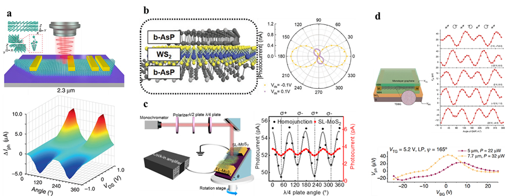
    In 2020,Lei Tong et al. utilized high-mobility,narrow-bandgap,anisotropic quasi-two-dimensional tellurium(Te)photodetectors to achieve target imaging with a linear polarization extinction ratio greater than 9 at the wavelength of 2.3 μm29. Fig. 1(a)shows the schematic device structure and the polarization-dependent photoresponse. The polarization detection based on individual anisotropic materials is very compact. The characteristics of the polarization detector,including linear polarization extinction ratio and response wavelength,rely on the anisotropic absorption of the material.

    (a)Schematic diagram of tellurium(Te)crystal structure. Schematic diagram of the device structure. At room temperature,the incident power is 6.0 mW,and the net polarized photocurrent ΔIph is when the incident wavelength is 2.3 μm[29];(b)Schematic diagram of the unipolar barrier van der Waals heterostructure photodetector composed of b-AsP/WS2/b-AsP. Polar plots of linear polarization angle-dependent forward-bias-driven photocurrent and reverse-bias-driven photocurrent[30];(c)Schematic diagram of the full-Stokes polarization measurement setup. Comparison of helicity-dependent photocurrents at 0 V and -0.1 V for homostructure devices and monolayer MoS2[31];(d)Schematic of a twisted double bilayer graphene(TDBG)photodetector. Photovoltage(Vph)as a function of the quarter-wave plate(QWP)angle(θ)at different gate voltage biases(VBG,VTG)measured at T = 79 K and λ = 5 µm. Photovoltage function of VBG excited by 5 µm and 7.7 µm linearly polarized light(LP)when ψ = 165° and VTG = 5.2 V[32]

    Figure 1.(a)Schematic diagram of tellurium(Te)crystal structure. Schematic diagram of the device structure. At room temperature,the incident power is 6.0 mW,and the net polarized photocurrent ΔIph is when the incident wavelength is 2.3 μm29;(b)Schematic diagram of the unipolar barrier van der Waals heterostructure photodetector composed of b-AsP/WS2/b-AsP. Polar plots of linear polarization angle-dependent forward-bias-driven photocurrent and reverse-bias-driven photocurrent30;(c)Schematic diagram of the full-Stokes polarization measurement setup. Comparison of helicity-dependent photocurrents at 0 V and -0.1 V for homostructure devices and monolayer MoS231;(d)Schematic of a twisted double bilayer graphene(TDBG)photodetector. Photovoltage(Vph)as a function of the quarter-wave plate(QWP)angle(θ)at different gate voltage biases(VBG,VTG)measured at T = 79 K and λ = 5 µm. Photovoltage function of VBG excited by 5 µm and 7.7 µm linearly polarized light(LP)when ψ = 165° and VTG = 5.2 V32

    In 2022,Wenjie Deng et al. constructed a twisted unipolar barrier van der Waals heterostructure using the anisotropic material b-AsP30. The heterostructure consisted of a b-AsP/WS2/b-AsP configuration,forming a small barrier for electrons and a high barrier for holes to create a unipolar barrier by band engineering. The bias-switchable photocurrents are dominated by the anisotropic absorption at the top and bottom,respectively. The device realizes full polarization state detection of linearly polarized incident light in the mid-infrared band. The linear polarization extinction ratio is 55 under the bias of 0.1 V. Fig. 1(b)shows the structure diagram of the heterojunction device and the polarization photocurrent under the external bias. Anisotropic two-dimensional materials are commonly used for linear polarization detection,and heterojunctions can be constructed based on these materials to enhance their anisotropic absorption through band engineering. However,achieving circular polarization detection using two-dimensional materials is challenging.

    In 2021,Chen Fang et al. demonstrated the use of inherent in-plane and out-of-plane optical anisotropy of MoS2 to fabricate a full-Stokes polarimeter on a single-layer MoS2/few-layer MoS2 homojunction chip. This homojunction on-chip full-Stokes polarimeter is based on valley-dependent optical selection rules in monolayer MoS2,which induces valley-locked spin-polarized photocurrent known as the circular photogalvanic effect(CPGE). The response is further enhanced by the monolayer MoS2/few-layer MoS2 homojunction,enabling the detection of all four Stokes parameters of incident light at zero bias in the 650 ~ 690 nm wavelength range31. Chen Fang et al. employed mechanical rotation to achieve an oblique incidence of light on the surface of an isotropic single-layer MoS2/few-layer MoS2 homojunction. Fig. 1(c)shows the schematic diagram of the homojunction device test and the photocurrent as the function of the angle of the quarter-wave plate.

    In 2022,Chao Ma et al. achieved a breakthrough in realizing a tunable mid-infrared bulk photovoltaic effect by utilizing twisted double bilayer graphene(TDBG)at 5 μm and 7.7 μm wavelengths32. The TDBG device benefits from the strong symmetry-breaking properties of the graphene moiré superlattice material,as well as the nonlinear light-matter interaction regulated by quantum geometry. Additionally,the advanced machine learning algorithm,such as a convolutional neural network(CNN),is applied to recognize the double-gate-dependent bulk photovoltaic voltage mapping and achieve the full Stokes polarization reconstruction32.

    1.2 linear and circular photogalvanic effect in topology materials

    Topological materials exhibit novel optoelectronic phenomena due to their unique electronic band structure,involving the Berry curvature of the electron wavefunction32. Topological materials generate prominent photocurrent under linear and/or circular polarized light with broken inversion symmetry or time-reversal symmetry. These phenomena are known as the linear photogalvanic effect(LPGE)and circular photogalvanic effect(CPGE),respectively. Besides,topological semimetals hold promise for broadband infrared detection due to their gapless band structure at the Weyl point.

    In 2018,Su-Yang Xu et al. demonstrated the tunable Berry curvature dipole of single-layer topological insulator WTe2 to realize observable and electrically switchable CPGE33. The low-energy band structure of monolayer WTe2 without spin-orbit coupling features tilted two-dimensional Dirac fermions at the Q and Q’ points. The CPGE is induced by interband transitions of the inverted quantum spin Hall(QSH)gap near the Q and Q’ points located close to the bottom of the conduction band. The inverted band structure and tilted crystal lattice of monolayer WTe2 produce Berry curvature dipoles and strong electric field effects,resulting in an observable and electrically switchable CPGE for circularly polarized light detection.

    In 2018,Jiawei Lai et al. developed a self-powered photodetector with broadband capabilities,utilizing a type-II Weyl semimetal Td-MoTe2. The anisotropy of this material is wavelength-dependent,with greater anisotropy at excitation wavelengths closer to the Weyl node. Td-MoTe2 is a promising material for broadband polarization-sensitive and self-powered photodetection with excellent response. Based on the anisotropy of Td-MoTe2,there are anisotropic photocurrent responses at different linear polarization excitation of 10.6 μm,4 μm,and 633 nm,and the linear polarization extinction ratios are 2.72,1.92 and 1.19,respectively22. Afterward in 2022,Junchao Ma et al. conducted a study on the semiconductor material Te. They discovered that under 10.6 μm and 4.0 μm photoexcitation,the material exhibited opposite CPGE directions due to the chirality-dependent optical selection rules for transitions between the valence band and the conduction band of the semiconductor material Te between Weyl cones23.

    In 2019,Gavin B. Osterhoudt et al. employed the topological structure of Weyl semimetal TaAs and focused ion beam(FIB)manufacturing technology to achieve the giant bulk photovoltaic effect(BPVE)in the 10.6 µm band at room temperature34. The investigation of the nonlinear optical properties of TaAs revealed that the CPGE is related to electronic chirality in TaAs.

    (a)False-color scanning electron microscope image of a TaAs device. Along the a-axis and c-axis,the photocurrent varies with the angle of the quarter-wave plate[34];(b)Schematic experimental set-up for detecting the mid-infrared circular photogalvanic effect on a dual-gated monolayer WTe2 device. Polarization along the a-axis depends on the photocurrent[33];(c)The lattice structure of tellurium(Te). The quarter-wave plate-dependent photocurrent at the position of the maximum positive and negative response of the Te device under 10.6 μm(middle)and 4 μm(bottom)excitation[23];(d)Optical microscope image of the MoTe2 device. Crystal structure of Td-MoTe2. Anisotropic photocurrent response with a polarization extinction ratio of 2.72 for linearly polarized excitation at 10.6 μm[22]

    Figure 2.(a)False-color scanning electron microscope image of a TaAs device. Along the a-axis and c-axis,the photocurrent varies with the angle of the quarter-wave plate34;(b)Schematic experimental set-up for detecting the mid-infrared circular photogalvanic effect on a dual-gated monolayer WTe2 device. Polarization along the a-axis depends on the photocurrent33;(c)The lattice structure of tellurium(Te). The quarter-wave plate-dependent photocurrent at the position of the maximum positive and negative response of the Te device under 10.6 μm(middle)and 4 μm(bottom)excitation23;(d)Optical microscope image of the MoTe2 device. Crystal structure of Td-MoTe2. Anisotropic photocurrent response with a polarization extinction ratio of 2.72 for linearly polarized excitation at 10.6 μm22

    1.3 Chiral perovskite and organic materials

    Chiral materials are defined as objects that cannot be superimposed on their mirror images. Due to their distinct chiral properties,they find diverse applications in fields such as medicine,biology,and quantum technology35. The differential absorption of left-handed circularly polarized light(LCP)and right-handed circularly polarized light(RCP)by chiral perovskite and organic materials offers the opportunity to directly detect circularly polarized light(CPL).

    In 2019,Chao Chen et al. fabricated a CPL detector using chiral organic-inorganic hybrid(α-PEA)PbI3 perovskite. To synthesize the chiral perovskite,they selected chiral α-phenylethylamine,whose π bond on the benzene ring aids in the positional interaction between the chiral amine and the(PbI64- matrix,enhancing the CPL-sensitive absorption. The circularly polarized detector exhibited a maximum polarization extinction ratio of 1.1 around the wavelength of 395 nm,a responsivity of 797 mA/W-1,and a detectivity of 7.1 × 10¹¹ Jones36. The device remained stable for one month. Although direct detection of CPL was achieved,the circular polarization extinction ratio(CPER)is not sufficient.

    In 2020,A. Ishii et al. fabricated a CPL detector using the helical one-dimensional(1D)structure of lead halide perovskite,which is composed of naphthyl ethylamine-based chiral organic cations37. The 1D structure consists of face-sharing(PbI64- octahedral chains,and R-(+)- and S-(-)-1-(1-naphthyl)ethylamine were chosen as the chiral cations in the 1D perovskites. The helicity of the 1D structure is primarily influenced by the chiral cations,resulting in an extremely high CPER. This work reported the highest CPER(25.4 at the wavelength of 395 nm)of perovskite based circular polarization detectors.

    In 2021,Zhen Liu et al. incorporated chiral organic ligands into the inorganic octahedral framework(PbX64- of perovskite to create an optically active chiral hybrid perovskite(CHP)with efficient charge transport38. The chiral ligand has a large π bond on the benzene ring,facilitating the Coulomb interaction between the chiral amine and the(PbI64- matrix,which enhances CPL-sensitive absorption. They fabricated CPL detectors with high photocurrent and polarization selectivity using CHP single-crystal nanowire arrays. The CPL detectors exhibited a CPER of 1.27,an on-off ratio of 1.8×10⁴,and a responsivity of 1.4 A/W-1 at 510 nm with a bias voltage of 5 V.

    In 2022,Yang Cao et al. created a new van der Waals heterojunction by combining a two-dimensional chiral hybrid perovskite material(MBA)2PbI4 with black phosphorus(BP)39. The interfacing perovskite provides an inflow of numerous photogenerated carriers to BP,to reinforce the charge carrier transfer,separation,and transport processes. The responsivity and photogain of BP in heterostructures are boosted by almost one order of magnitude with respect to BP alone,which is more obvious under excitation above the bandgap of perovskite. The linear polarized light extinction ratio of the van der Waals heterojunction reaches 9 at a wavelength of 1 550 nm.

    (a)Chiral hybrid perovskite(CHP)single-crystal array design for high-performance CPL direct photodetection[38];(b)Schematic of the photodetector. Crystal structure of(R- and S-α-PEA)PbI3. Circular dichroism(CD)and absorbance spectra of(R-,S-,and rac-α-PEA)PbI3 thin films[36];(c)Schematic diagram of a helical one-dimensional perovskite-based photodetector. J-V curves of(R-NEA)PbI3 device under LCP and RCP with a wavelength of 395 nm and an intensity of 1.0 mW cm-2[37];(d)Schematic diagram and crystal structure of vdW heterostructure photodetector device based on BP and chiral perovskite MPI. Electron and hole transfer process of MPI/BP heterostructure under 1550 nm illumination. Heterostructure output curves and individual BPs. Polar plot of the normalized polarization photocurrent measured at an illumination power of 100 μW and a wavelength of 1550 nm[39]

    Figure 3.(a)Chiral hybrid perovskite(CHP)single-crystal array design for high-performance CPL direct photodetection38;(b)Schematic of the photodetector. Crystal structure of(R- and S-α-PEA)PbI3. Circular dichroism(CD)and absorbance spectra of(R-,S-,and rac-α-PEA)PbI3 thin films36;(c)Schematic diagram of a helical one-dimensional perovskite-based photodetector. J-V curves of(R-NEA)PbI3 device under LCP and RCP with a wavelength of 395 nm and an intensity of 1.0 mW cm-2[37;(d)Schematic diagram and crystal structure of vdW heterostructure photodetector device based on BP and chiral perovskite MPI. Electron and hole transfer process of MPI/BP heterostructure under 1550 nm illumination. Heterostructure output curves and individual BPs. Polar plot of the normalized polarization photocurrent measured at an illumination power of 100 μW and a wavelength of 1550 nm39

    2 Integration of polarization-selective optical coupling structures

    In the previous section,the detection of linearly and/or circularly polarized light is based on polarization-sensitive materials,such as anisotropic two-dimensional materials,topological materials,and chiral perovskites or organic materials. However,the choice of these materials is quite limited. Poor chemical stability,low responsivity,and low polarization extinction ratio are the main problems for polarization detectors based on polarization-sensitive materials. On the other hand,artificial micro-nano optical structures show great potential in controlling the interaction between polarized light and matter. The polarization detectors with polarization-selective optical coupling structures,as well as the integration with anisotropic materials,show better performance in responsivity and polarization extinction ratio.

    2.1 Polarization-selective optical coupling structures

    Plasmonic structures play an important role in the interaction between light and matter. They enhance the polarization-dependent optoelectronic coupling through resonant excitation of localized surface plasmons. Therefore,plasmonic structures are important tools for achieving polarization-selective coupling. Different resonances with the enhanced localized optical field can be realized under specific polarizations of the incident light and then the polarization light is discriminated. Integration of the polarization-selective optical coupling structures and infrared detection materials can greatly improve polarization detection performance.

    In 2014,Qian Li et al. introduced a new approach to creating a grating plasmonic microcavity quantum well infrared detector by combining a single quantum well with a grating plasmonic microcavity40. The quantum well is employed as the active structure within the near-field region of the plasmonic effect enhanced cavity,with the localized surface plasmon(LSP)mode and the surface plasmon polariton(SPP)mode being controlled. The artificial plasma modulation significantly influences the propagation and distribution of light within the plasma microcavity,resulting in a high infrared polarization resolution capability for the grating plasmonic microcavity quantum well infrared detection device. Moreover,the device achieves an extinction ratio of 65 at 14.7 µm.

    In 2015,Wei Li et al. utilized a periodic array of chiral metamolecules comprised of a ‘Z’-shaped silver antenna on a poly(methyl methacrylate)spacer and an optically thick silver backplane to create a chiral plasmonic nanostructure with hot electron injection41. Plasmonic nanostructures with engineered chirality can differentiate between left-handed circularly polarized(LCP)and right-handed circularly polarized(RCP)light,and photodetection is based on hot electron injection into silicon. The chiral plasmonic nanostructure circular polarization detector achieves a polarization extinction ratio of 3.4 at the wavelength of 1 340 nm.

    In 2019,Mengjia Wang et al. employed gold-coated helical carbon nanowire end-fired and dipolar aperture nanoantennas to fabricate circularly polarized photodetectors by rotating surface plasmons on the subwavelength scale and utilizing optical spin-orbit interactions42. The device allows for adjustable polarization control with a CPER of 64 at 1 550 nm,indicating that circularly polarized light can be locally achieved by applying the concept of a helical traveling wave antenna to a single plasmonic nanoantenna.

    In 2020,Qiao Jiang et al. utilized an asymmetric n-shaped gold nanoantenna chiral plasmonic metasurface integrated with a single layer of MoSe2 to create an ultra-thin circular polarimeter43. The chiral plasmonic metasurface is utilized to selectively detect circularly polarized light,while the two-dimensional material determines the working wavelength range(visible to near-infrared). The circular polarization-dependent photocurrent response based on the left-handed and right-handed metasurfaces is verified. The ultra-thin circular polarimeter achieves an extinction ratio of 1.74 for the left-handed metasurface and 1.9 for the right-handed metasurface at the wavelength of 790 nm.

    (a)SEM image of the cleaved facet of the cavity structure. SEM image of PCQWID,a grating plasmonic microcavity quantum well infrared detector. The relationship between the average intensity of the photocurrent measured at the wavelength of 14.2 ~ 14.9 µm and the polarization angle of the incident light[40];(b)Schematic of the chiral metamaterial and CPL detector. Experimentally measured circular dichroism spectra of the left-handed(LH,blue)and right-handed(RH,red)metamaterials[41];(c)HTN schematic and how it works. The ellipticity factor of the output beam of the helical traveling wave nanoantenna HTN and the experimental spectrum of the DOCP. Polarization state analysis at wavelengths of 1.55 μm and 1.64 μm[42];(d)Schematic illustration of the hybrid structure consisting of a chiral plasmonic metasurface and monolayer MoSe2. Optical absorption spectra of left-handed and right-handed plasmonic metasurfaces illuminated by light.[43]

    Figure 4.(a)SEM image of the cleaved facet of the cavity structure. SEM image of PCQWID,a grating plasmonic microcavity quantum well infrared detector. The relationship between the average intensity of the photocurrent measured at the wavelength of 14.2 ~ 14.9 µm and the polarization angle of the incident light40;(b)Schematic of the chiral metamaterial and CPL detector. Experimentally measured circular dichroism spectra of the left-handed(LH,blue)and right-handed(RH,red)metamaterials41;(c)HTN schematic and how it works. The ellipticity factor of the output beam of the helical traveling wave nanoantenna HTN and the experimental spectrum of the DOCP. Polarization state analysis at wavelengths of 1.55 μm and 1.64 μm42;(d)Schematic illustration of the hybrid structure consisting of a chiral plasmonic metasurface and monolayer MoSe2. Optical absorption spectra of left-handed and right-handed plasmonic metasurfaces illuminated by light.43

    2.2 Integration of anisotropic material and polarization-selective optical coupling structures

    Combining the advantages of polarization-selective optical coupling structures and the anisotropic absorption in materials,the integration of polarization-selective plasmonic cavities and anisotropic materials exhibits a double enhancement of polarization discrimination.

    In 2018,Yuwei Zhou et al. integrated an array of anisotropic plasmonic microcavity(PMC)with a quantum well infrared detector. PMC structures manipulate photonic modes at a sub-wavelength scale to enhance the photoelectric coupling and increase the absorption of quantum wells44. The double polarization selection mechanism of the PMC and the quantum wells enhance the linear polarization extinction ratio up to 136 in the long wavelength infrared regime. Fig. 5(a)shows the schematic diagram of the three-dimensional simulation of the plasma microcavity quantum well infrared detector and the reconstruction of the Stokes parameters.

    (a)Schematic diagram of 3D simulation of plasmonic microcavity quantum well infrared detector.(b)Resolution of Stokes parameters[44];(c)Schematic diagram of the asymmetric composite structure.(d)Absorption and reflection spectra of anisotropic dielectric composite structures under LCP and RCP illumination[45]

    Figure 5.(a)Schematic diagram of 3D simulation of plasmonic microcavity quantum well infrared detector.(b)Resolution of Stokes parameters44;(c)Schematic diagram of the asymmetric composite structure.(d)Absorption and reflection spectra of anisotropic dielectric composite structures under LCP and RCP illumination45

    In 2020,Zeshi Chu et al. integrated asymmetric metamaterials on quantum wells for a long-wave infrared circular polarization detector. Based on the double polarization selection mechanism,a CPER of 14 is obtained45. This value is 10 times higher than that of the asymmetric metamaterial integrated HgCdTe detector. HgCdTe is the most widely used infrared detection material46-47. However,the CPER of the asymmetric metamaterial integrated HgCdTe detector is much lower since there is no double polarization selection. The double polarization selection mechanism is generally applicable to a variety of devices. When the asymmetric metamaterial is integrated with another anisotropic infrared detection material(InAsSb nanowire array),the CPER of this device is 12.6 in the mid-infrared region. In comparison,when the same asymmetric metamaterial is integrated into an InAsSb bulk material,the CPER is only 1.7. In addition,the integration of anisotropic optoelectronic materials and asymmetric metamaterials yields an improved CPER without compromising the absorptivity of active materials. High-intensity photonic modes excited by the asymmetric metamaterials can increase the absorption in the active materials by several times. Fig. 5(b)shows the schematic composite structure of the asymmetric metamaterial and the detection material. and the absorption and reflection spectra of the anisotropic composite structure under left-handed circularly polarized light and right-handed circularly polarized light.

    The bowtie antenna and aligned single-walled carbon nanotube(SWCNT)films integrated infrared detector,proposed by our research group,can be utilized for highly polarization-sensitive far-infrared detection,with a polarization extinction ratio exceeding 13 600 at a resonance frequency of 0.5 THz48. Our proposed plasmonic microcavity-integrated graphene photodetector for polarization detection achieves a polarization extinction ratio of approximately 30 at a wavelength of 1.55 µm49-50. In addition,the research group has also designed quantum well infrared photodetectors(QWIPs)integrated with all-semiconductor strip plasmonic cavities with high polarization sensitivity,and the polarization extinction ratio exceeds 900 in the terahertz band51. In the long-wave range,our proposed asymmetric metamaterial integrated quantum well(anisotropic material)has a CPER of approximately 14 45. This CPER is twice as high as that observed for graphene integrated with chiral plasmonic nanoantenna electrodes in the mid-infrared band52.

    2.3 Configurable photocurrent polarity by the optical structure

    By integrating polarization-sensitive materials with micro-nano optical structures,high responsivity,and polarization extinction ratio has been achieved. Recently,configurable photocurrent polarity has also been realized by integrating plasmonic nanoantennas. The polarity of photocurrent can be tuned by light polarization flexibly and an infinite extinction ratio is realized at the polarity-transition point. In such cases,the traditional definition of polarization extinction ratio is no longer applicable,and the corresponding extinction ratio at the photocurrent polarity-transition approaches infinity.

    (a)Scanning electron microscope image of a thermopile element. Measured thermoelectric reactor emf voltage(black dots)as a function of incident light ellipticity angle χ compared to normalized S3 Stokes parameters at a wavelength of 7.9 µm and a light intensity of 270 W cm-2[53];(b)Device schematic for spin-controlled unidirectional plasmonic waveguide on-chip electrical detection. A Soleil-Babinet variable phase retarder was employed to convert linearly polarized laser radiation into left and right circular polarization states of intermediate elliptical and orthogonal linear polarization states[54];(c)Schematic of a metasurface-mediated graphene photodetector. I-V curves of the device under dark and light conditions[55];(d)Schematic of a nanoantenna-mediated semimetal photodetector. Measured(symbols)and fitted(dashed lines)photovoltage versus polarization angle for different gate voltages[56];(e)Symmetry analysis of the photoresponse of an achiral plasmonic nanostructure located on a graphene sheet. Measured I-V curve with drain-source bias. Illustration of a CPL-specific photodetector in a Poincaré sphere,where the photovoltage Vph depends only on the fourth Stokes parameter S3 of the incident light[57]

    Figure 6.(a)Scanning electron microscope image of a thermopile element. Measured thermoelectric reactor emf voltage(black dots)as a function of incident light ellipticity angle χ compared to normalized S3 Stokes parameters at a wavelength of 7.9 µm and a light intensity of 270 W cm-2[53;(b)Device schematic for spin-controlled unidirectional plasmonic waveguide on-chip electrical detection. A Soleil-Babinet variable phase retarder was employed to convert linearly polarized laser radiation into left and right circular polarization states of intermediate elliptical and orthogonal linear polarization states54;(c)Schematic of a metasurface-mediated graphene photodetector. I-V curves of the device under dark and light conditions55;(d)Schematic of a nanoantenna-mediated semimetal photodetector. Measured(symbols)and fitted(dashed lines)photovoltage versus polarization angle for different gate voltages56;(e)Symmetry analysis of the photoresponse of an achiral plasmonic nanostructure located on a graphene sheet. Measured I-V curve with drain-source bias. Illustration of a CPL-specific photodetector in a Poincaré sphere,where the photovoltage Vph depends only on the fourth Stokes parameter S3 of the incident light57

    In 2016,Feng Lu et al. placed the thermal junction of a thermocouple at the center of an optical antenna to create an antenna-coupled thermopile photodetector53. The device is only sensitive to light ellipticity,and an antenna-coupled thermopile photodetector is used to convert the degree of circular polarization of light into a DC voltage proportional to the S3 Stokes parameter of the incident radiation. The detector produces a bipolar voltage output that is proportional to the S3 Stokes parameter of the incident light in the 7 ~ 9 µm wavelength range. The detector design is completely achiral,indicating that the incident light’s chirality is converted into either the current direction or the DC voltage sign in the detector.

    In 2019,Martin Thomaschewski et al. combined strong light-matter interactions in plasmons with semiconductor technology based on spin-orbit interactions in achiral plasmonic nanocircuits54. They achieved this by integrating two gold-germanium-gold chiral plasmonic waveguide photodetectors,resulting in a compact polarimeter capable of detecting the circular polarization light.

    In 2021,Jingxuan Wei et al. developed nanoantenna-mediated few-layer graphene photodetectors. The device allows for configurable switching between unipolar and bipolar polarization dependence of linear polarization response in the mid-infrared region through vectorial and nonlocal photoresponses55-56. The orientation of the nanoantenna in the device can be adjusted to vary the polarization extinction ratio from positive to negative,covering all possible values,with the polarization extinction ratio approaching infinity at the polarity-transition point. This enables linearly polarized light detection with a range from finite to infinite extinction ratio.

    Recently,in 2022,Jingxuan Wei et al. developed a mid-infrared circular polarization detection device by integrating plasmonic nanostructure arrays and graphene ribbons57. The geometric arrangement of plasmonic nanostructures enhances circularly polarized light detection,and the photocurrent generated by the achiral structure achieves a CPER of 84 under zero bias in the mid-infrared band at room temperature. The detection of CPL should be robust,with immunity against the ubiquitous unpolarized and linearly polarized light.

    (a)SEM image of a polarimeter. Polar plot of photoresponse as a function of quarter-wave plate(QWP)rotation angle[58];(b)SEM image of the device. Simulations and experiments examine the intensity of the 0° and 135° linearly polarized light(LP)components as a function of the half-wave plate(HWP). Simulations and experiments examine the intensity of different QWP angles for left-handed circularly polarized light(LCP)and right-handed circularly polarized light(RCP)components[59];(c)False-color SEM image of a fiber end-face stack. One cycle photocurrent of the twisted BP cell as a function of QWP angle[60];(d)Schematic diagram of on-chip phase demodulation for high-speed coherent optical communication. The normalized output intensities of different waveguide ports for a single nanodisk element and two double nanodisk elements were experimentally measured and simulated[61];(e)Structural design of resonant thermoelectric photoresponse. Polarization-angle-dependent photoresponse simulations(lines)and measurements(symbols)for five typical devices. Simulated(line)and measured(symbol)photoresponses of four typical devices as a function of QWP angle[62]

    Figure 7.(a)SEM image of a polarimeter. Polar plot of photoresponse as a function of quarter-wave plate(QWP)rotation angle58;(b)SEM image of the device. Simulations and experiments examine the intensity of the 0° and 135° linearly polarized light(LP)components as a function of the half-wave plate(HWP). Simulations and experiments examine the intensity of different QWP angles for left-handed circularly polarized light(LCP)and right-handed circularly polarized light(RCP)components59;(c)False-color SEM image of a fiber end-face stack. One cycle photocurrent of the twisted BP cell as a function of QWP angle60;(d)Schematic diagram of on-chip phase demodulation for high-speed coherent optical communication. The normalized output intensities of different waveguide ports for a single nanodisk element and two double nanodisk elements were experimentally measured and simulated61;(e)Structural design of resonant thermoelectric photoresponse. Polarization-angle-dependent photoresponse simulations(lines)and measurements(symbols)for five typical devices. Simulated(line)and measured(symbol)photoresponses of four typical devices as a function of QWP angle62

    3 Challenge and opportunity: on-chip full-stokes detection

    On-chip infrared polarization detection has been extensively studied nowadays. The perception of a single polarization state has been thoroughly studied. Full Stokes detection that includes all polarization information becomes a challenge and opportunity.

    In 2020,Lingfei Li et al. developed four metasurface-integrated graphene-silicon photodetectors based on the geometric chirality and anisotropy of the metasurface for circular and linear polarization-resolved light responses58. The photodetector enables full Stokes parameter detection for arbitrary polarized incident infrared light at 1 550 nm.

    In 2021,Changyu Zhou et al. coupled four single-mode silicon waveguides to a circle-like polarization distinguishing device on an insulating silicon substrate to create an on-chip optical polarimeter capable of measuring arbitrary polarization states59.

    In 2022,Yifeng Xiong et al. developed a fiber-integrated polarimeter by vertically stacking three photodetection units based on two-dimensional vdW materials on the fiber end face60. The polarimeter consists of six layers of van der Waals materials stacked vertically to form three photodetection units. Two anisotropic BP units are twisted stacked for polarized light sensing,and a bismuth selenide(Bi2Se3)layer provides power calibration. The polarimeter features self-power-calibration,self-driven,and ambiguity-free detection of linearly and circularly polarized light by breaking symmetry-induced LPGEs and CPGEs in the two BP units.

    In 2022,Ting Lei et al. coupled a network of single-mode Si waveguides to an insulating silicon substrate to achieve on-chip high-speed coherent optical signal detection based on photon spin-orbit interactions and enable full Stokes parameter measurement of incident light61.

    In 2022,Mingjin Dai et al. integrated plasmonic chiral materials and two-dimensional thermoelectric materials to prepare an on-chip mid-infrared photodetector62. The photodetector is based on the polarization-dependent photothermal effect in chiral plasmonic metamaterial-mediated and the Seebeck effect of two-dimensional thermoelectric materials. It enables the detection of linearly polarized and circularly polarized light and realizes on-chip full Stokes detection in the mid-infrared band at room temperature. However,the average measurement errors are large. The error of S1,S2,and S3 are 14.2%,15.2%,and 5.4%,respectively. More accurate on-chip full-Stokes detection is desired.

    4 Conclusion

    Many different approaches and significant efforts have been dedicated to the advances of on-chip infrared polarization detectors. These polarization detectors can be realized by polarization-sensitive materials including anisotropic two-dimensional materials,topological materials,chiral materials,and integrated polarization-selective optical coupling structures. When polarization-selective optical coupling structures and polarization selective detection materials are combined in a proper way,high polarization discrimination can be achieved. With the development of artificial metamaterials-mediated detectors,the polarity of photocurrent can be flexibly tuned by light polarization,and an infinite extinction ratio could be realized at the polarity-transition point. In conclusion,on-chip polarization detection by integrating anisotropic materials and optical structure has received widespread attention. In the future,on-chip full Stokes parameters detection with high accuracy of all polarization states covering the full Poincare sphere presents challenges and opportunities.

    References

    [1] J S Tyo, D L Goldstein, D B Chenault et al. Review of passive imaging polarimetry for remote sensing applications. Applied Optics, 45, 5453(2006).

    [2] L Li, W Han, L Pi et al. Emerging in‐plane anisotropic two‐dimensional materials. InfoMat, 1, 54-73(2019).

    [3] Y Wang, P Wu, Z Wang et al. Air‐Stable Low‐Symmetry Narrow‐Bandgap 2D Sulfide Niobium for Polarization Photodetection. Advanced Materials, 32, 2005037(2020).

    [4] M I Beddiar, X Zhang, B Liu et al. Ambipolar-To-Unipolar Conversion in Ultrathin 2D Semiconductors. Small Structures, 3, 2200125(2022).

    [5] M Buscema, D J Groenendijk, S I Blanter et al. Fast and Broadband Photoresponse of Few-Layer Black Phosphorus Field-Effect Transistors. Nano Letters, 14, 3347-3352(2014).

    [6] Y Liu, T Sun, W Ma et al. Highly responsive broadband black phosphorus photodetectors. Chinese Optics Letters, 16, 020002(2018).

    [7] D J Perello, S H Chae, S Song et al. High-performance n-type black phosphorus transistors with type control via thickness and contact-metal engineering. Nature Communications, 6, 7809(2015).

    [8] N Mao, J Tang, L Xie et al. Optical Anisotropy of Black Phosphorus in the Visible Regime. Journal of the American Chemical Society, 138, 300-305(2016).

    [9] F W Han, C X Zhao, Y M Zhang. Photoelectric properties of monolayer black phosphorus in visible regime at room temperature. AIP Advances, 9, 055216(2019).

    [10] T Hong, B Chamlagain, W Lin et al. Polarized photocurrent response in black phosphorus field-effect transistors. Nanoscale, 6, 8978-8983(2014).

    [11] X Chen, X Lu, B Deng et al. Widely tunable black phosphorus mid-infrared photodetector. Nature Communications, 8, 1672(2017).

    [12] T Akamatsu, T Ideue, L Zhou et al. A van der Waals interface that creates in-plane polarization and a spontaneous photovoltaic effect. Science, 372, 68-72(2021).

    [13] Y Deng, Z Luo, N J Conrad et al. Black Phosphorus–Monolayer MoS2 van der Waals Heterojunction p–n Diode. ACS Nano, 8, 8292-8299(2014).

    [14] P Chen, J Xiang, H Yu et al. Gate tunable MoS2–black phosphorus heterojunction devices. 2D Materials, 2, 034009(2015).

    [15] X Jiang, M Zhang, L Liu et al. Multifunctional black phosphorus/MoS2 van der Waals heterojunction. Nanophotonics, 9, 2487-2493(2020).

    [16] T Hu, R Zhang, J-P Li et al. Photodetectors based on two-dimensional MoS2 and its assembled heterostructures. Chip, 1, 100017(2022).

    [17] J Bullock, M Amani, J Cho et al. Polarization-resolved black phosphorus/molybdenum disulfide mid-wave infrared photodiodes with high detectivity at room temperature. Nature Photonics, 12, 601-607(2018).

    [18] A Rasmita, C Jiang, C Jiang et al. Tunable geometric photocurrent in van der Waals heterostructure. Optica, 7, 1204-1208(2020).

    [19] Y Chen, Y Wang, Z Wang et al. Unipolar barrier photodetectors based on van der Waals heterostructures. Nature Electronics, 4, 357-363(2021).

    [20] P Wu, L Ye, L Tong et al. Van der Waals two-color infrared photodetector. Light: Science & Applications, 11, 6(2022).

    [21] C Chen, X Lu, B Deng et al. Widely tunable mid-infrared light emission in thin-film black phosphorus. Science Advances, 6, eaay6134(2020).

    [22] J Lai, X Liu, J Ma et al. Anisotropic Broadband Photoresponse of Layered Type-II Weyl Semimetal MoTe2. Advanced Materials, 30, 1707152(2018).

    [23] J Ma, B Cheng, L Li et al. Unveiling Weyl-related optical responses in semiconducting tellurium by mid-infrared circular photogalvanic effect. Nature Communications, 13, 1-7(2022).

    [24] R Wang, L Li, H Tian et al. Full telecomband covered half-wave meta-reflectarray for efficient circular polarization conversion. Optics Communications, 427, 469-476(2018).

    [25] J Zhou, J Deng, M Shi et al. Cavity coupled plasmonic resonator enhanced infrared detectors. Applied Physics Letters, 119, 160504(2021).

    [26] F Jiang, M Shi, J Zhou et al. Integrated Photonic Structure Enhanced Infrared Photodetectors. Advanced Photonics Research, 2, 2000187(2021).

    [27] W Chen, Z Zhao, C Wang et al. Linear polarization grating combining a circular polarization grating with a special cycloidal diffractive quarter waveplate. Optics Express, 27, 33378-33390(2019).

    [28] R Zhou, K Ullah, S Yang et al. Recent advances in graphene and black phosphorus nonlinear plasmonics. Nanophotonics, 9, 1695-1715(2020).

    [29] L Tong, X Huang, P Wang et al. Stable mid-infrared polarization imaging based on quasi-2D tellurium at room temperature. Nature Communications, 11, 2308(2020).

    [30] W Deng, M Dai, C Wang et al. Switchable Unipolar-Barrier Van der Waals Heterostructures with Natural Anisotropy for Full Linear Polarimetry Detection. Advanced Materials, 34, 2203766(2022).

    [31] C Fang, J Li, B Zhou et al. Self-Powered Filterless On-Chip Full-Stokes Polarimeter. Nano Letters, 21, 6156-6162(2021).

    [32] C Ma, S Yuan, P Cheung et al. Intelligent infrared sensing enabled by tunable moiré quantum geometry. Nature, 604, 266-272(2022).

    [33] S-Y Xu, Q Ma, H Shen et al. Electrically switchable Berry curvature dipole in the monolayer topological insulator WTe2. Nature Physics, 14, 900-906(2018).

    [34] G B Osterhoudt, L K Diebel, M J Gray et al. Colossal mid-infrared bulk photovoltaic effect in a type-I Weyl semimetal. Nature Materials, 18, 471-475(2019).

    [35] C Zhang, X Wang, L Qiu. Circularly Polarized Photodetectors Based on Chiral Materials: A Review. Frontiers in Chemistry, 9, 711488(2021).

    [36] C Chen, L Gao, W Gao et al. Circularly polarized light detection using chiral hybrid perovskite. Nature Communications, 10, 1927(2019).

    [37] A Ishii, T Miyasaka. Direct detection of circular polarized light in helical 1D perovskite-based photodiode. Science Advances, 6, eabd3274(2020).

    [38] Z Liu, C Zhang, X Liu et al. Chiral Hybrid Perovskite Single‐Crystal Nanowire Arrays for High‐Performance Circularly Polarized Light Detection. Advanced Science, 8, 2102065(2021).

    [39] Y Cao, C Li, J Deng et al. Enhanced photodetector performance of black phosphorus by interfacing with chiral perovskite. Nano Research, 15, 7492-7497(2022).

    [40] Q Li, Z Li, N Li et al. High-Polarization-Discriminating Infrared Detection Using a Single Quantum Well Sandwiched in Plasmonic Micro-Cavity. Scientific Reports, 4, 6332(2015).

    [41] W Li, Z J Coppens, L V Besteiro et al. Circularly polarized light detection with hot electrons in chiral plasmonic metamaterials. Nature Communications, 6, 8379(2015).

    [42] M Wang, R Salut, H Lu et al. Subwavelength polarization optics via individual and coupled helical traveling-wave nanoantennas. Light: Science & Applications, 8, 76(2019).

    [43] Q Jiang, B Du, M Jiang et al. Ultrathin circular polarimeter based on chiral plasmonic metasurface and monolayer MoSe2. Nanoscale, 12, 5906-5913(2020).

    [44] Y W Zhou, Z F Li, J Zhou et al. High extinction ratio super pixel for long wavelength infrared polarization imaging detection based on plasmonic microcavity quantum well infrared photodetectors. Scientific Reports, 8, 15070(2018).

    [45] Z Chu, J Zhou, X Dai et al. Circular Polarization Discrimination Enhanced by Anisotropic Media. Advanced Optical Materials, 8, 1901800(2020).

    [46] W Hu, Z Ye, L Liao et al. 128 × 128 long-wavelength/mid-wavelength two-color HgCdTe infrared focal plane array detector with ultralow spectral cross talk. Optics Letters, 39, 5184-5187(2014).

    [47] W D Hu, X S Chen, Z H Ye et al. A hybrid surface passivation on HgCdTe long wave infrared detector with in-situ CdTe deposition and high-density hydrogen plasma modification. Applied Physics Letters, 99, 091101(2011).

    [48] B Chen, Z Ji, J Zhou et al. Highly polarization-sensitive far infrared detector based on an optical antenna integrated aligned carbon nanotube film. Nanoscale, 12, 11808-11817(2020).

    [49] S Guo, D Zhang, J Zhou et al. Enhanced infrared photoresponse induced by symmetry breaking in a hybrid structure of graphene and plasmonic nanocavities. Carbon, 170, 49-58(2020).

    [50] D Zhang, J Zhou, C Liu et al. Enhanced polarization sensitivity by plasmonic-cavity in graphene phototransistors. Journal of Applied Physics, 126, 074301(2019).

    [51] J Deng, Y Zheng, J Zhou et al. Absorption enhancement in all-semiconductor plasmonic cavity integrated THz quantum well infrared photodetectors. Optics Express, 28, 16427(2020).

    [52] J Peng, B P Cumming, M Gu. Direct detection of photon spin angular momentum by a chiral graphene mid-infrared photodetector. Optics Letters, 44, 2998(2019).

    [53] F Lu, J Lee, A Jiang et al. Thermopile detector of light ellipticity. Nature Communications, 7, 12994(2016).

    [54] M Thomaschewski, Y Yang, C Wolff et al. On-Chip Detection of Optical Spin–Orbit Interactions in Plasmonic Nanocircuits. Nano Letters, 19, 1166-1171(2019).

    [55] J Wei, Y Li, L Wang et al. Zero-bias mid-infrared graphene photodetectors with bulk photoresponse and calibration-free polarization detection. Nature Communications, 11, 6404(2020).

    [56] J Wei, C Xu, B Dong et al. Mid-infrared semimetal polarization detectors with configurable polarity transition. Nature Photonics, 15, 614-621(2021).

    [57] J Wei, Y Chen, Y Li et al. Geometric filterless photodetectors for mid-infrared spin light. Nature Photonics, 17, 171-178(2022).

    [58] L Li, J Wang, L Kang et al. Monolithic Full-Stokes Near-Infrared Polarimetry with Chiral Plasmonic Metasurface Integrated Graphene–Silicon Photodetector. ACS Nano, 14, 16634-16642(2020).

    [59] C Zhou, Y Xie, J Ren et al. Spin separation based on-chip optical polarimeter via inverse design. Nanophotonics, 11, 813-819(2022).

    [60] Y Xiong, Y Wang, R Zhu et al. Twisted black phosphorus-based van der Waals stacks for fiber-integrated polarimeters. Science Advances, 8, eabo0375(2022).

    [61] T Lei, C Zhou, D Wang et al. On-Chip High-Speed Coherent Optical Signal Detection Based on Photonic Spin-Hall Effect. Laser & Photonics Reviews, 16, 2100669(2022).

    [62] M Dai, C Wang, B Qiang et al. On-chip mid-infrared photothermoelectric detectors for full-Stokes detection. Nature Communications, 13, 4560(2022).

    Yu-Ran ZHEN, Jie DENG, Yong-Hao BU, Xu DAI, Yu YU, Meng-Die SHI, Ruo-Wen WANG, Tao YE, Gang CHEN, Jing ZHOU. Recent advances in on-chip infrared polarization detection[J]. Journal of Infrared and Millimeter Waves, 2024, 43(1): 52
    Download Citation