The complex band structures of a 1D anisotropic graphene photonic crystal are investigated, and the dispersion relations are confirmed using the transfer matrix method and simulation of commercial software. It is found that the result of using effective medium theory can fit the derived dispersion curves in the low wave vector. Transmission, absorption, and reflection at oblique incident angles are studied for the structure, respectively. Omni-gaps exist for angles as high as 80° for two polarizations. Physical mechanisms of the tunable dispersion and transmission are explained by the permittivity of graphene and the effective permittivity of the multilayer structure.
Graphene is a flat monolayer of graphite with carbon atoms closely packed in a 2D honeycomb lattice [1,2]. The most important features of graphene are that its conductivity or dielectric function can be tuned by the chemical potential of the graphene sheets via electrostatic biasing. One application for graphene is to tune absorption properties of dielectric photonic crystals. A single layer of graphene can absorb as much as 2.3% of the incident light in a wide range of frequencies [3]. The absorption can be greatly enhanced by placing a monolayer of graphene on top of a 1D Si/SiO2 photonic crystal [4] or on top of 1D parity-time symmetric photonic crystals [5]. Near-perfect single-band [6] and dual-band [7] absorption can be achieved by inserting a graphene layer as a defect layer in the asymmetric 1D photonic crystal.
A 1D graphene-based photonic crystal (GPC) usually refers to an artificial periodic array composed of alternating graphene and dielectric materials [8]. A complex 1D GPC was proposed by periodically embedding the 1D traditional GPC into a background medium [9]. A 1D GPC has wide applications in tunable devices, such as biosensors [10], terahertz modulators [11], polarizers [12,13], antenna radomes [14], narrowband filters [15], and so on. Moreover, surface plasmon polaritons (SPPs) can exist in 1D GPC and show a high degree of subwavelength localization. It is possible to control the scattering of SPPs in 1D GPC with inhomogeneous doping [16] and to obtain low-loss plasmonic supermodes by coupling SPPs in each graphene sheet [17,18]. Finally, it is interesting that a 1D GPC exhibits properties of hyperbolic metamaterials, such as epsilon-near-zero phenomena [19], the tunable localized [20,21] and long-wavelength Tamm SPPs [22], negative refraction with superior transmission [23], and critical coupling effect [24].
For 1D GPC composed of alternating graphene and dielectric materials, the transmission [8,25–30] and dispersion relation [12,31–33] have been investigated by using the transfer matrix method (TMM) in which graphene is considered as a conductor sheet without thickness or an isotropic material. Actually, graphene is a uni-axial anisotropic material with permittivity a tensor for its 2D nature [34,35]. By investigating dispersion and transmission characteristics of 1D anisotropic GPC, the application of terahertz amplification is proposed [34]. Waveguide modes are described for 1D anisotropic GPC through the Comsol Multiphysics software with the finite element method, and hyperbolic dispersion characteristics are found [35]. Besides, the defect modes of 1D anisotropic GPC are investigated [36,37]. The transmission characteristic of 1D anisotropic GPC with symmetrical dual-layer defects is studied and found to have applications in tunable multiband filters [36]. The defect mode can also be created by inserting a 1D anisotropic GPC as a defect layer in 1D dielectric photonic crystal [37]. Dispersion relations of 1D anisotropic GPC discussed above [34,35] are usually obtained by treating the periodic structure as a homogeneous effective medium with anisotropic permittivity. Actually, for the dispersion relation of 1D anisotropic GPC, the Bloch vector in graphene is complex due to the inherent absorption of the graphene. Then, dispersion relations are divided into two parts: the real part and imaginary part corresponding to the propagating and evanescent Bloch waves, respectively.
Sign up for Photonics Research TOC. Get the latest issue of Photonics Research delivered right to you!Sign up now
In this work, the complex photonic band structures of 1D GPC composed of alternating anisotropic graphene and dielectric materials are discussed. First, dispersion relations are derived without using effective medium theory (EMT). Then, dispersion properties are confirmed by transmission curves with the TMM and commercial software. It is found that the result using EMT only fit the dispersion curves in the region of a low wave vector. Transmission, absorption, and reflection at oblique incident angles are studied for the 1D anisotropic GPC, respectively. Omni-gaps are found for angles as high as 80° for the two polarizations. The physical mechanisms of the tunable dispersion relations at normal incidence are explained based on the graphene permittivity and the effective permittivity theory for 1D anisotropic GPC.
2. THEORETICAL MODEL AND FORMULATIONS
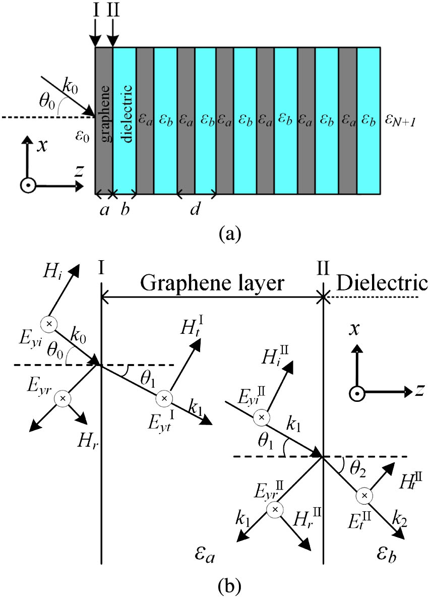
The schematic view of an obliquely incident electromagnetic wave in 1D GPC is shown in Fig. 1(a). The layers are oriented in the plane, and electromagnetic waves propagate along the plane with wave vector and incident angle . The permittivity of graphene and dielectric are and with thicknesses of and , respectively. is the period. and are the dielectric permittivity in the input and output plane for periodic structure with numbers of period. The boundary surface between input plane and graphene is named I, while that between graphene and dielectric is named II. The incident wave can be divided into the TE polarization with and , and the TM polarization with and . Figure 1(b) shows the field distribution of the TE polarization.
Figure 1.(a) Schematic view of oblique wave in 1D GPC. (b) Field distribution of TE polarization in the graphene layer.
Graphene is an optically uni-axial anisotropic material because of its 2D nature, whose permittivity tensor can be given by (when graphene lies in the plane) [34,35]
The normal component of graphene permittivity is , as the normal electric field cannot excite any current in the graphene sheet [34]. The tangential component of graphene permittivity is expressed as [38] Here, is the angular frequency, is the permittivity in vacuum. is the surface conductivity of graphene, and and are the intraband conductivity and the interband conductivity and are defined in the following: where is the charge of an electron, is the chemical potential with carrier density , and the Femi velocity of electrons . is the phenomenological scattering rate, is the Kelvin temperature, is Boltzmann’s constant, and ⏧ is the reduced Plank’s constant.
A. Transfer Matrix Equation for TM Polarization
The transmission characteristics of the GPC can be described by the TMM [38]. In the case of TM polarization with and , and can be connected by a transfer matrix between boundary I and II [36]: where , .
Likewise, the transfer matrix in a dielectric layer can be written as where , , .
B. Transfer Matrix Equation for TE Polarization
In the case of TE polarization with and , the Maxwell curl equations in this case are
Eliminating and from these equations, we can obtain satisfying the equation
The dispersion relation of TE polarization in the anisotropic graphene is calculated For boundary I and II, and can be connected by the transfer matrix where .
Likewise, the transfer matrix in a dielectric layer can be written as where , , .
C. Transmission, Reflection, and Absorption
The transfer matrix of the TM or TE polarization for one period can be written as
Then, for periods, the electromagnetic field in the input and output boundary can be written as where and are the electric and magnetic field in the output boundary, are the elements of the matrix .
The refection coefficient and transmission coefficient are given by where where and are the relative dielectric constants of the dielectric in the input and output plane, respectively, and are angles in the input and output plane; in our calculation, vacuum is used both in the input and output plane.
The refection coefficient and transmission coefficient and absorption are written as
D. Dispersion Equation
Dispersion equation of 1D GPC can be described from Eq. (15): where represents the sum of diagonal elements of , and represents a complex wave vector in the direction. The real part and imaginary part are corresponding to the propagating and evanescent Bloch waves, respectively. If we rewrite the real and imaginary parts as and for the right side in Eq. (19), respectively. That means . Then, the real part and imaginary part of the dispersion equation can be rewritten in the form [39], respectively, where
3. RESULTS AND DISCUSSION
For normal incidence, the transmission and dispersion of the TM and TE polarizations are the same and not affected by the normal component of graphene permittivity as . We assume the dielectric is quartz with a relative permittivity of and thickness μ. The graphene has parameters of the chemical potential of , thickness , temperature and scattering rate [40,41].
Figure 2 shows the dispersion relations of the 1D GPC at normal incidence based on dispersion equations. Figure 2(a) shows the dispersion in the real part of using Eq. (20). It is seen that there are two photonic band gaps (PBGs): the first gap locates from 7.15 to 7.87 THz, and the second gap ranges from 14.3 to 14.71 THz. The Fabry–Perot limit is ( is an integer) for the single dielectric layer (without graphene sheet). It is noticed that the frequencies at the low edges of the two gaps are equal to the Fabry–Perot frequencies for and 2. This observation is consistent with the theory for a mesh grid–dielectric stack at microwaves [42]. Figure 2(b) shows the imaginary part of , which indicates the damping using Eq. (21). It is seen that the higher imaginary components coincide with the corresponding gaps in the real part of dispersion. One notices that the value of imag [] between 0–2.3 THz is quite high and is similar with the metallic band gap in metal–dielectric photonic crystal [43]; we call it the graphene band gap, and is the cut-off frequency. The two gaps in the high frequencies determined by the periodic structure belong to the structure band gaps.
Figure 2.Dispersion relation of the 1D GPC at normal incidence. (a) Real part. (b) Imaginary part.
To confirm the dispersion relation of the 1D anisotropic GPC. Figures 3(a)–3(c) show the transmission, reflection, and absorption curves calculated by two methods. The dashed line denotes the result with the TMM method, and the dotted line is the simulation result using the commercial software (CST Microwave Studio) based on the finite-difference time domain (FDTD) technique. They are almost overlapped together, except a little difference in the graphene band gap, and the two structure band gaps are all in accordance with these in the dispersion relation. It is worth mentioning that these fast oscillations outside of the band gaps are the Fabry–Perot oscillations of Bloch waves making round-trips upon reflection at the multilayer boundaries [44]. The insert in Fig. 3(c) shows the 3D simulation model with periods in the transmission direction of the axis. The lengths in the and directions are both 10 μm. The open boundary condition is employed along the direction while periodic boundary conditions are employed along the and directions. A frequency domain solver is selected to obtain the transmission and reflection . The absorption is obtained through .
Figure 3.Transmission, reflection, and absorption curves using the TMM (solid line) and CST simulation (dotted line). Insert shows the simulation model with periods.
In the presence of the complex frequency dependence of graphene permittivity, it is not possible to define an analytical expression for the cut-off to predict the transparency in 1D GPC as the 1D metallic photonic crystal [45,46]. In the following, we can show that dispersion in the low frequency is consistent with that of using EMT. The effective medium permittivity of the GPC can be obtained based on Maxwell–Garnett approach [47]. Here we define is the filling factor of the graphene; then is the filling factor of the dielectric.
The effective dispersion relations of the 1D GPC for TM and TE polarization can be derived as [48] where , are the permittivity components of the composite parallel and perpendicular to the graphene surface, respectively.
For normal incidence at , the effective dispersion relation for the TM and TE polarizations reduces to
Figure 4 shows the dispersion curve using the EMT method and the dispersion equation for TM and TE polarizations. The dash–dot, dash, and dot lines are dispersion curves using dispersion equation for , 40°, and 80°, respectively. The solid line with the same color shows results using the EMT method. In Fig. 4(a), the real part of the dispersion using dispersion equations is almost in accordance with that using the EMT method except the higher value near the first gap for the EMT method. For the imaginary part of the dispersion in Fig. 4(b), higher values are obtained below the cut-off frequency for the EMT method. Therefore, dispersion relations of 1D anisotropic GPC can be obtained by using an effective medium method [34,35]; however, the result can fit the dispersion curves using dispersion equations only in the low wave vector.
Figure 4.Dispersion curves of TM and TE polarization using EMT method (solid line) and dispersion equation. (a) Real part. (b) Imaginary part.
Photonic crystals can prohibit propagation of electromagnetic waves whose frequencies lie within the PBGs. The PBGs are usually different for TE and TM polarizations at different incident angles. If photonic crystal is designed to exhibit 100% reflectivity at any angle of incidence for both TE and TM polarizations [49,50], such a structure is generally known as omni-directional photonic crystal and omni-directional PBGs. Figure 5 shows color maps of transmission, absorption, and the difference of reflection and absorption versus frequencies and incident angles for TM and TE polarizations using the TMM method, where the oblique incidence varies from 0° to 90°. It is seen that the structure exhibits almost omnidirectional PBGs for the first two gaps. The two omnidirectional PBGs shift to the higher frequencies with little variation of the width as the incident angle increases; the first gap shifts more slowly than the second one. The cut-off frequency changes little below for the two polarizations. All the transmissions are in agreement with the dispersion relation in Fig. 4. In Fig. 5(b), the absorption of the two polarizations tends to decrease with the frequency increasing. The largest absorption appears near the cut-off frequency. The larger absorptions locate at the high edges of the two gaps caused by the absorption of graphene layer, and the absorption magnitude is almost angle-independence. As the lower edges of the gaps are determined by the Fabry–Perot resonance of the structure, then little absorption is obtained. Figure 5(c) shows the difference between the refection and the absorption A with value of . The black regions are corresponding to the values of . It is seen that the larger reflections appear in regions of the graphene band gap, the structure gaps, and the regions with incident angles larger than 80°. The absorption is larger than the reflection at the high edges of the gaps and the regions with higher transmission.
Figure 5.Color map of (a) transmission, (b) absorption, and (c) the difference of reflection and absorption versus frequencies and incident angles for TM and TE polarizations.
A. Influence of Chemical Potential on Dispersion and Transmission
As seen in Eq. (2), surface conductivity of the graphene depends on the chemical potential. The chemical potential can be tuned by the external gate voltages applied on graphene layers. Then, the dispersion and propagation properties of 1D GPC can be further adjusted by the biased voltages on graphene layers. Moreover, the chemical potential could also be tuned by the electric field, magnetic field, and chemical doping [51]. Figure 6 shows the dispersion relations under different chemical potential at normal incidence. The dash–dot, solid, and doted lines denote the results of , 0.5, and 0.9 eV, respectively. It is seen that the cut-off frequency and the gaps shift to the higher frequencies with gap width enlarged, and the magnitude of the imaginary part increases as increase from 0.1 to 0.9 eV. Figure 7 shows the corresponding transmission, absorption, and difference of absorption and reflection. As increases, the transmission decreases while the cut-off frequency and the gaps increase, and the absorption tends to increase and shift to the higher frequencies, the refection increases at the two gaps and below the cut-off frequencies.
Figure 6.Dispersion relation for chemical potential , 0.5, and 0.9 eV. (a) Real part. (b) Imaginary part.
Figure 8 shows the color maps of transmission and absorption versus different chemical potentials at normal incidence using the TMM. For the transmission, as increases, the cut-off frequency shifts to the higher frequency and width of the two gaps increase. Location of the low edge of the two gaps change little because they are determined by the Fabry–Perot resonance of the dielectric layer, while the high edges shift to the higher frequency. For the absorption, the largest absorption always appears near the cut-off frequencies, and the larger absorptions appear near the high edges of the two gaps. These absorptions shift to the higher frequency with their width increase as increases.
Figure 8.Color map of (a) transmission and (b) absorption for different .
To explain these properties of dispersion and transmissions at normal incidence, Fig. 9(a) shows the real part and imaginary part of graphene tangential component versus chemical potential using Eq. (2). It should be noted that the graphene permittivity is only determined by its tangential component at normal incidence. In the frequencies of 0–20 THz, the real part is negative, while the imaginary part is positive. They both strongly depend on the frequency in the low frequencies and vary slowly in the high frequencies. The absolute value of the graphene tangential permittivity increases as chemical potential increases. The larger difference of dielectric function between graphene and dielectric enlarges the gap [52]. On the other hand, the variation of the cut-off frequency and the first gap is larger than in the second gap, as the graphene permittivity becomes larger in the low frequencies.
Figure 9.Influence of the chemical potential on real and imaginary part of (a) graphene tangential permittivity and (b) effective dielectric constant of the multilayer for normal incidence.
Figure 9(b) shows the real and imaginary parts of the effective permittivity using the effective dispersion relations of Eqs. (22) and (23), where for normal incidence. It is seen that the real part decreases as chemical potential increases. According to the variational principle [53], decreasing of dielectric constant leads to increasing of frequency modes; then, the dispersion shifts toward the higher frequencies. The imaginary part of effective permittivity is close to 0 at frequencies larger than 6 THz, while it has large increases below 6 THz, which would give rise to the larger absorption in the low frequencies. As the larger imaginary part of the effective permittivity shifts to the higher frequency with increasing, the absorption correspondingly shifts.
4. CONCLUSION
The dispersion relations of 1D anisotropic GPC composed of alternative graphene and dielectric layers are derived based on the TMM method. The complex band structures under oblique incidence are investigated. Dispersion properties of the 1D anisotropic GPC are confirmed by transmission curves with the TMM and commercial software. For the dispersion in the real part, the frequencies at the low edges of the two gaps are equal to the Fabry–Perot frequencies. The dispersion in the imaginary part indicates the damping, and the higher imaginary components coincide with the corresponding gaps in the real part of dispersion. It is also found that the dispersion using the EMT can fit the result obtained from the dispersion equations in the low frequency. Furthermore, almost omnidirectional and polarization-independent PBGs can be found in the structure. Tunable dispersion and transmission properties versus chemical potential are explained by the graphene permittivity as well as the effective permittivity of the GPC structure.
[5] P. Cao, X. Yang, S. Wang, Y. Huang, N. Wang, D. Deng, C. Liu. Ultrastrong graphene absorption induced by one-dimensional parity-time symmetric photonic crystal. IEEE Photon. J., 9, 1-9(2017).
[49] V. Kumar, A. Kumara, K. H. S. Singh, P. Kumar. Broadening of omni-directional reflection range by cascade 1D photonic crystal. Optoelectron. Adv. Mater., 5, 488-490(2011).
[50] J. P. Pandey. Enlargement of omnidirectional reflection range using cascaded photonic crystals. Int. J. Pure Appl. Phys., 13, 167-173(2017).