
Zehong Wan, Enkang Cui, Shengtao Yu, Yu Lei, Chengqun Gui, Shengjun Zhou. Effects of Reactive Ion Etching Parameters on Etching Rate and Surface Roughness of 4H-SiC[J]. Laser & Optoelectronics Progress, 2021, 58(19): 1922002
- Laser & Optoelectronics Progress
- Vol. 58, Issue 19, 1922002 (2021)
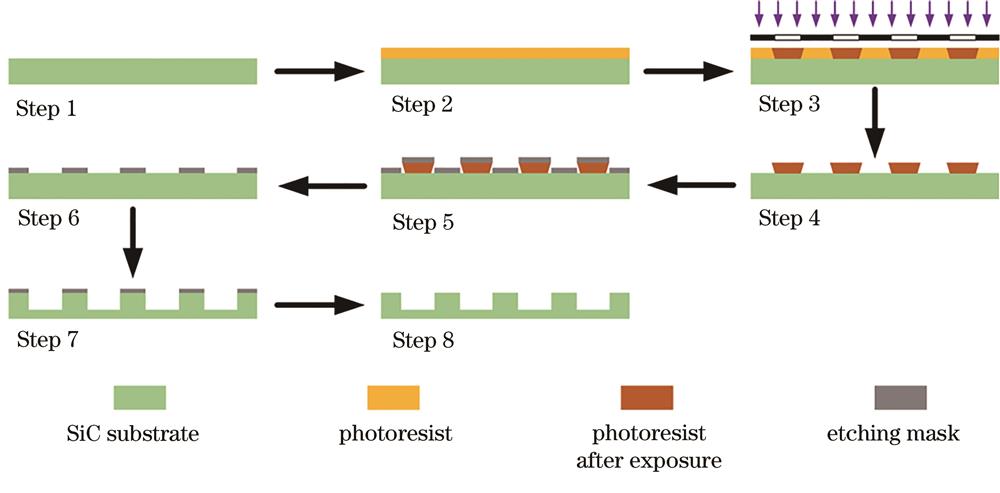
Fig. 1. Schematic illustration of experimental flow (Step 1: 4H-SiC substrate cleaning; Step 2: photoresist spin coating; Step 3: exposure; Step 4: development; Step 5: coating; Step 6: lift-off; Step 7: RIE; Step 8: mask removing and 4H-SiC substrate cleaning)
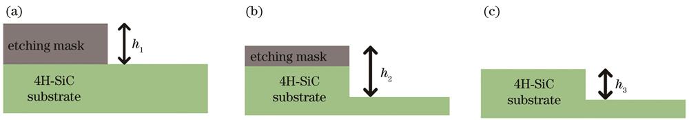
Fig. 2. Schematic illustration of step height measurement. (a) Step height
Fig. 3. SEM images of different photoresists after exposure and development. (a) S1818 photoresist; (b) AR-N4340 photoresist; (c) ROL-7133 photoresist; (d) AZ2070 photoresist
Fig. 4. Influence of exposure mode on photolithography. (a) Schematic illustration of exposure; (b) optical microscopy image of graphic photoresist in micro-force contact exposure mode; (c) optical microscopy image of graphic photoresist in soft contact exposure mode
Fig. 5. Optical microscopy images of patterned photoresist with different exposure time and development time.(a)‒(c) Exposure time is 5, 10, and 20 s, respectively, and development time is kept at 20 s; (d)‒(e) exposure time is kept at 20 s, and development time is 16 and 20 s, respectively
Fig. 6. Optical microscopy images of etching masks obtained after coating and lift-off of 4H-SiC substrates with poor and good lithographic quality. (a) Poor lithographic quality; (b) good lithographic quality
Fig. 7. SEM images of 4H-SiC substrate after etching. (a) C-face; (b) Si-face
Fig. 8. Influence of etching time. (a)‒(c) Height difference
Fig. 9. Schematic illustration of actually measured step height. (a) Step height
Fig. 10. Influence of etching time after process improvement. (a) Etching rate of 4H-SiC substrate; (b) etching rate of Ni mask; (c) RIE etching selection ratio of Ni to 4H-SiC; (d)‒(f) SEM images of SiC after etching 200, 400, and 600 s, respectively
Fig. 11. Effect of O2 content on 4H-SiC etching rate and surface RMS roughness
Fig. 12. Effect of chamber pressure on 4H-SiC etching rate and surface RMS roughness
Fig. 13. Effect of RF power on 4H-SiC etching rate and surface RMS roughness

Set citation alerts for the article
Please enter your email address
© Copyright 2018-2021 | Chinese Laser Press. All Rights Reserved 沪ICP备15018463号-20