
Yongkang Xu, Sannian Song, Wencheng Fang, Chengxing Li, Zhitang Song. The etching process and mechanism analysis of Ta-Sb2Te3 film based on inductively coupled plasma[J]. Journal of Semiconductors, 2020, 41(12): 122103
- Journal of Semiconductors
- Vol. 41, Issue 12, 122103 (2020)
Abstract
1. Introduction
Phase change memory can realize the transformation between polycrystalline and amorphous by using the ordered and disordered changes of phase change materials under the action of heat induction, and the data storage by using the obvious resistance difference between the ordered and disordered two states[
In the process of VLSI fabrication, the etching process is to convert the graphics on the mask into the actual graphics. With the development of semiconductor technology, wet etching has been unable to meet the processing requirements of nanoscale fine lines due to its inherent limitations. Dry etching has gradually developed. In dry etching, the inductively coupled plasma (ICP) etching method has been widely used in semiconductor technology due to its high ion density, good etching uniformity, high etching perpendicularity and good finish. ICP etching is an etching method that combines physical ion bombardment with a chemical reaction. Compared with the traditional reactive ion etching method (RIE), ICP etching has great advantages, which can control the plasma density and plasma energy respectively[
Previous study shows that Cl-based plasma has a high anisotropy. But the ICP etching by Cl-based plasma currently has a low etch rate and selectivity[
In this work, a mixture of CF4 and Ar was used to systematically study the etching process of the new phase change material Ta-Sb2Te3, and the etching parameters such as the ratio of CF4/Ar, the pressure in the etching chamber and the incident power applied on the bottom electrode were optimized. Finally, the optimal etching process parameters of the Ta-Sb2Te3film were obtained.
2. Methods of experiment
In this work, the preparation method of phase change material films is the magnetron sputtering method, and the preparation method is a multi-functional vacuum sputtering system. Thermal SiO2 with a thickness of 500 nm was used as the substrate material. The device is equipped with four sputtering targets, two RF power sources and two DC power sources, each of which can be selected. During sputtering, the element ratio of the film is controlled by adjusting the sputtering power of the corresponding target, and the thickness of the film is controlled by the sputtering time. The equipment is equipped with five channels of gas, the flow of which can be precisely controlled by the flow meter. The photoresist mask layer was then prepared on the film surface by UV lithography. The etching system used in the experiment is a ULVAC NE-550H type inductively coupled plasma device, which provides high-density plasma from a high-power RF source (13.56 MHz). The surface morphology was examined by a scanning electron microscope (SEM). Besides, X-ray photoelectron spectroscopy (XPS) will be applied on the etched Ta-Sb2Te3 surface to explain the etching mechanism of the Ta-Sb2Te3.
3. Results and discussion
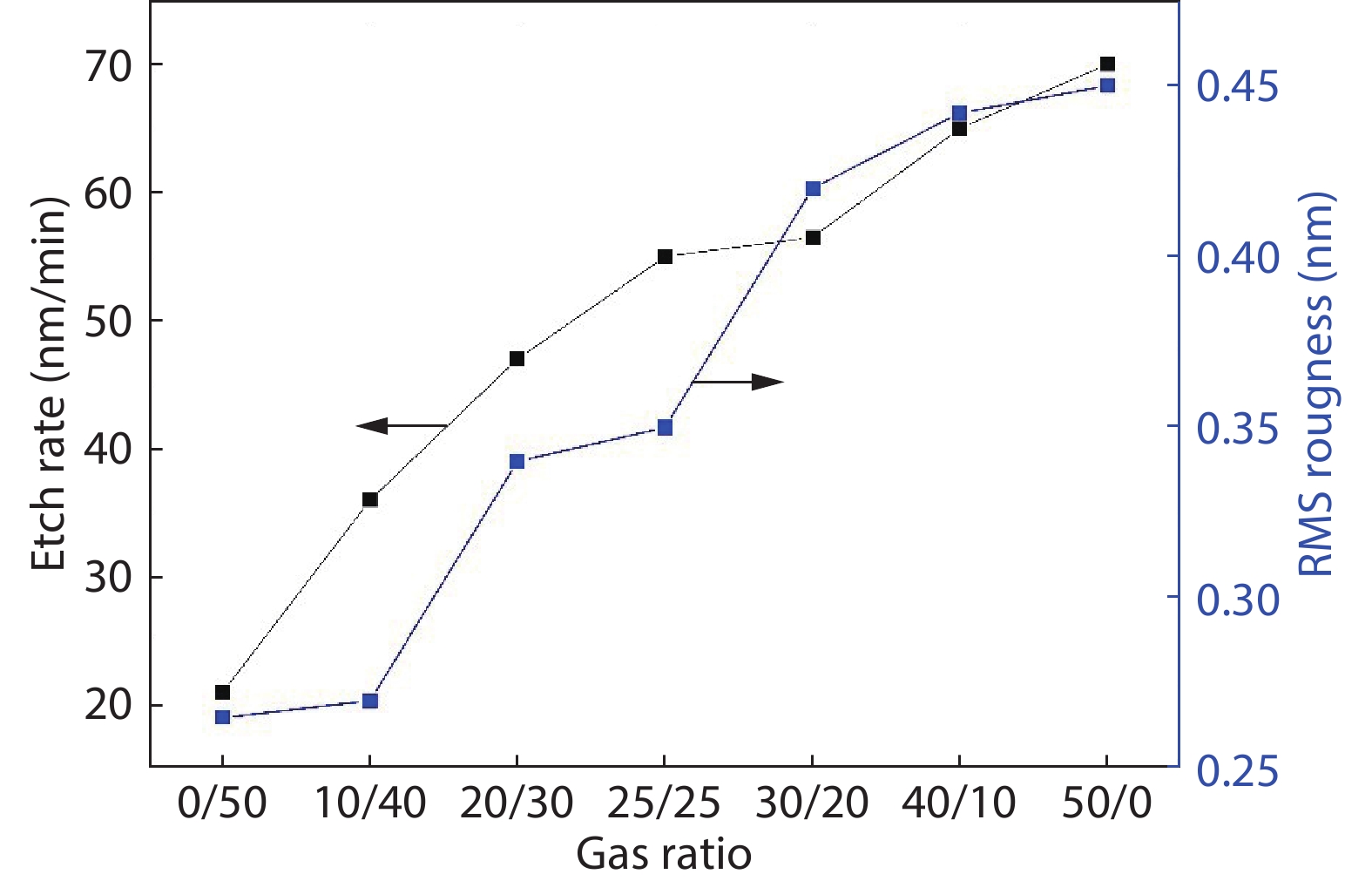
Firstly, the effects of CF4/Ar of different components on etching rate and surface roughness were studied. F plasma mainly acted as a chemical reaction, while Ar acted as a physical bombardment to increase the anisotropy of etching. In this experiment, we used 600 W ICP power and 2.5 Pa chamber pressure to conduct experimental research on different CF4/Ar ratio. As can be seen from Fig. 1, the etching rate tends to increase gradually with the increase of the composition of F-based gas. This is mainly because with the increase of F-based gas, the chemical reaction is enhanced and the etching rate is improved. However, as the concentration of CF4 continues to increase, the concentration of the chemical F ion will also increase, and the non-volatile substances in the etching products will accumulate on the sample surface in large quantities. The physical bombardment of Ar ion cannot take away the non-volatile by-products in the chemical reaction, and a micro mask will be formed on the sample surface, resulting in increased surface roughness.
![]()
Figure 1.Effect of gas composition on etching rate and surface roughness.
The surface morphonology of Ta-Sb2Te3 after the ICP etching process was measured by AFM with a scan area of 1 × 1 μm2(Fig. 2). It can be seen that, under the action of CF4/Ar, the surface roughness shows an increasing trend. After ICP etching, as the concentration of CF4 increases, the RMS roughness increased from 0.27 to 0.442 nm, suggesting that this technique roughens the surface.
![]()
Figure 2.(Color online) AFM images of Ta-Sb2Te3 surface (a) CF4/Ar = 10/40, RMS = 0.27, (b) CF4/Ar = 20/30, RMS = 0.34, (c) CF4/Ar = 25/25, RMS = 0.35, (d) CF4/Ar = 30/20 and RMS = 0.42.
After the etch gas enters the etch chamber, molecules, atoms, excited state substances, electrons, positive ions, negative ions, free radicals, UV and visible light will be generated through the excitation, dissociation, ionization and other reactions of the electric field magnetic field in the etch chamber. After entering the etching chamber, CFx* ions and F− are mainly generated. CF4 → CFx* + (4−x) F− (x ≤ 3). According to Table 1 fluoride boiling points, a reaction may occur in the etching chamber.
Therefore, we speculate that under the action of CF4/Ar, certain non-volatile fluoride products will be produced on the surface of the sample film, resulting in increased surface roughness.
Taking the surface morphonology and etching rate into consideration, the optimized recipe with 25 sccm CF4 and 25 sccm Ar was chosen. Fig. 3 shows the effect of chamber pressure on etching rate and characteristic of Ta-Sb2Te3 using the optimized parameters above (CF4 = 25 sccm, Ar = 25 sccm, ICP source power = 600 Pa). Under the condition of constant gas flow, ICP power and temperature in the etching chamber, the pressure in the etching chamber is changed, and the etching rate decreases with the increase of pressure. As the pressure increases, the chance of plasma collision in the etching cavity increases. After the collision, the speed of the plasma slows down, and the force of its bombardment on the substrate is greatly weakened, leading to a decrease in the etching rate.
![]()
Figure 3.Effect of chamber pressure on etching rate and surface roughness.
During the etching process, the steepness of the sidewall has the greatest impact on the device integration process. As demonstrated in Figs. 4(a)–4(e), the ICP etching profile is observed to become more vertical with the increase of chamber pressure. The SEM image of the sidewall of the Ta-Sb2Te3 thin film etched under the conditions of CF4/Ar = 25/25, ICP power of 600 W is shown in Fig. 4. It can be seen that, when chamber pressure reaches 2.5 Pa, the verticality of the etched section is optimum. As demonstrated in Fig. 4(f), the steepness of the sidewalls is observed as it decreases. Therefore, the optimal etching pressure is 2.5 Pa. When chamber pressure is lower than 2.5 Pa, physical bombardment plays a dominant role in the etching process, and the sidewall has low steepness and the sidewall is depressed by the physical bombardment. When chamber pressure is stronger than 2.5 Pa, the steepness of the etched sidewall begins to decrease. The reason may be that the chemical reaction process dominates under this etching condition, and the non-volatile substances generated by the reaction accumulate at the side wall, which affects the further progress of the etching process at the side wall position.
![]()
Figure 4.SEM of cross sections of Ta-Sb2Te3 after ICP etching with pressure of (a)1.0 Pa, (b) 1.5 Pa, (c) 2.0 Pa, (d) 2.25 Pa, (e) 2.5 Pa, (f) 2.75 Pa with CF4 flow of 25 sccm, Ar flow of 25 sccm, ICP power of 600 W.
The optimized process with 25/25 CF4/Ar flow and 2.5 Pa pressure was selected because of its advantage in etch rate and surface morphology. Several experiments with different ICP power settings were performed. Fig. 5 demonstrates that TaSb2Te3 etch rate mainly depended on ICP power. As ICP source power increases from 400 to 600 W, the ICP etching rate goes from 22 to 61 nm/min. Increasing ICP power increases the energy of the plasma and increases the chance of reacting with the substrate surface. Moreover, with the increase of plasma energy and the enhancement of physical bombardment, the probability of products being dropped from the substrate surface by plasma increases, and the etching rate is faster. With the increase of ICP power, the direction of plasma is strengthened, which makes the side wall become straight and clean. As the power continues to increase, the surface roughness after etching tends to increase, mainly because the increase of ICP power will lead to too much physical bombardment, affecting the sample surface flatness.
![]()
Figure 5.Effects of ICP source power on RMS roughness and etching rate of Ta-Sb2Te3.
In order to explore the reaction product residue on the film surface during the ICP etching and the damage to the sample, we conducted an XPS depth analysis test on the sample, as shown in Fig. 6. In the deep section process, the etching time of Ar ion was 0, 60, 120, and 180 s, respectively. The XPS instrument uses an Al Kα dual anode source with a photon energy of 1486.6 eV. The ion-gun energy and ion current of the XPS Ar+ ion gun were set to 2 kV and 20 μA. The etching rate is 1.3 nm/min. As shown in Fig. 6(a), the metal peak binding energy of Ta 2p is 23.08 and 26.50 eV, and the intensity of the metal peak increases with increasing bombardment time. As can be seen from Sb 3d in Fig. 6(b), there are peaks of 528.6 and 537.5 eV, which correspond to Sb–Te chemical bonds, and their peaks are stronger and stronger. The peak at 530.1 eV from Sb–F bonding in the spectrum of the film indicates that the sample has been fluorinated. As the etching time of Ar increased, the peak strength decreased, indicating that more Sb fluoride was generated in the film. With the increase of bombardment time, the fluorine peak strength of Sb3d decreases gradually, while the intensity of the metal peak increases with the increase of the bombardment time, which shows that during the etching process, Sb in the alloy is easy to etch, and its products are also easily taken away. These results correspond exactly to the boiling points of fluorides in Table 1. Fig. 6(c) shows the Te3d XPS narrow scan spectra. In Fig. 6(c), the peak intensity of Te3d before Ar bombardment is weaker than that after bombardment, which shows that most of the etching products of Te element have volatilized during the etching process, and the Te element content at the sample surface less than a certain depth. And the surface only has a peak of Te-Sb (the binding energy is 572.5 and 582.9 eV, respectively).
![]()
Figure 6.(Color online) XPS spectrum of each component of the Ta-Sb2Te3 film after ICP etching.
Therefore, it can be concluded that the residue on the etching surface of Ta-Sb2Te3 is mainly the fluoride of Sb, while the by-product of Te generated in the etching process is very volatile and does not have residues on the surface. The above analysis proved that using CF4/Ar as an etching gas has little damage to the Ta-Sb2Te3 thin film etching.
In order to verify the etching damage caused by ICP etching, XRD was used to analyze the change of the surface lattice before and after etching. High-resolution X-ray diffraction can obtain information such as lattice constant, full width at half maximum of diffraction peak, strain, relaxation, and accurate thickness measurement. Compared with before etching, the full width at half maximum of the diffraction peak changed after etching. Based on the results of XRD analysis in Fig. 7, it can be found that ICP etching with CF4/Ar can slightly widen the XRD half-peak width of the film in (006) crystal phase. It is inferred that the ICP etch using this optimized process had slight lattice damage to the Ta-Sb2Te3 film.
![]()
Figure 7.(Color online) XRD curves before and after ICP etching.
4. Conclusion
According to the theories of ICP etching, the optimized recipe with 600 W ICP power, 2.5 Pa pressure and 25/25 CF4/Ar flow was selected because of its good process repeatability. On this basis, the influence of mixed gas ratio on the steepness of the side wall was investigated, and the possible reactions and damage to the material in the etching process were analyzed from the angle of element composition and chemical bond. Under the scanning electron microscope (SEM) we have found that anisotropic profiles and smooth film surface can be obtained by the CF4/Ar gas mixture. Based on the above analysis, CF4/Ar is suitable as an etching gas for Ta-Sb2Te3.
Acknowledgements
This work was financially supported by the Natural Science Foundation of China (61874129) and the National Key Research and Development Program of China (2017YFB0405601).
References
[1] S R Ovshinsky. Reversible electrical switching phenomena in disordered structures. Phys Rev Lett, 21, 1450(1968).
[2] J S Washington, E A Joseph, S Raoux et al. Characterizing the effects of etch-induced material modification on the crystallization properties of nitrogen doped Ge2Sb2Te5. J Appl Phys, 109, 034502(2011).
[3] C Xu, B Liu, Z T Song et al. Reactive-ion etching of Sn-doped Ge2Sb2Te5 in CHF3/O2 plasma for non-volatile phase-change memory device. Thin Solid Films, 516, 7871(2008).
[4] Z T Song, S N Song, M Zhu et al. From octahedral structure motif to sub-nanosecond phase transitions in phase change materials for data storage. Sci China Inf Sci, 61, 081302(2018).
[5] F Rao, Z T Song, K Ren et al. Si–Sb–Te materials for phase change memory applications. Nanotechnology, 22, 145702(2011).
[6] J T Li, Y Y Xia, B Liu et al. Direct evidence of reactive ion etching induced damages in Ge2Sb2Te5 based on different halogen plasmas. Appl Surf Sci, 378, 163(2016).
[7] J T Li, Y Y Xia, B Liu et al. Etch characteristics and mechanism of TiSbTe thin films in inductively-coupled HBr-He, Ar, N2, O2 plasma. ECS J Solid State Sci Technol, 5, P330(2016).
[8] L L Shen, S N Song, Z H Zhang et al. Characteristics and mechanism of phase change material W0.03Sb2Te etched by Cl2/BCl3 inductively coupled plasmas. Thin Solid Films, 593, 67(2015).
[9] Z H Zhang, S N Song, Z T Song et al. Characteristics and mechanism of Al1.3Sb3Te etched by Cl2/BCl3 inductively coupled plasmas. Microelectron Eng, 115, 51(2014).
[10] S K Kang, M H Jeon, J Y Park et al. Etch damage of Ge2Sb2Te5 for different halogen gases. Jpn J Appl Phys, 50, 086501(2011).


Set citation alerts for the article
Please enter your email address

© Copyright 2018-2021 | Chinese Laser Press. All Rights Reserved 沪ICP备15018463号-20