• Journal of Semiconductors
  • Vol. 41, Issue 8, 082006 (2020)
Hengze Qu, Ziwei Lin, Ruijuan Guo, Xiyu Ming, Wenhan Zhou, Shiying Guo, Xiufeng Song, Shengli Zhang, and Haibo Zeng
Author Affiliations
  • Key Laboratory of Advanced Display Materials and Devices, Ministry of Industry and Information Technology, College of Material Science and Engineering, Nanjing University of Science and Technology, Nanjing 210094, China
  • show less
    DOI: 10.1088/1674-4926/41/8/082006 Cite this Article
    Hengze Qu, Ziwei Lin, Ruijuan Guo, Xiyu Ming, Wenhan Zhou, Shiying Guo, Xiufeng Song, Shengli Zhang, Haibo Zeng. First-principle study of puckered arsenene MOSFET[J]. Journal of Semiconductors, 2020, 41(8): 082006 Copy Citation Text show less

    Abstract

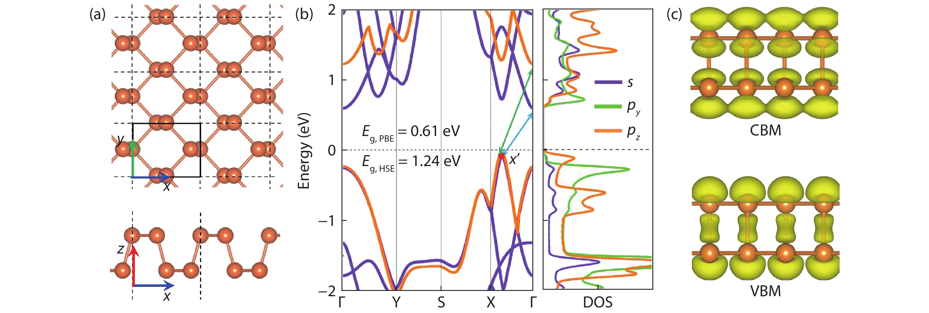
    Two-dimensional material has been regarded as a competitive silicon-alternative with a gate length approaching sub-10 nm, due to its unique atomic thickness and outstanding electronic properties. Herein, we provide a comprehensively study on the electronic and ballistic transport properties of the puckered arsenene by the density functional theory coupled with nonequilibrium Green’s function formalism. The puckered arsenene exhibits an anisotropic characteristic, as effective mass for the electron/hole in the armchair and zigzag directions is 0.35/0.16 m0 and 1.26/0.32 m0. And it also holds a high electron mobility, as the highest value can reach 20 045 cm2V–1s–1. Moreover, the puckered arsenene FETs with a 10-nm channel length possess high on/off ratio above 105 and a steep subthreshold swing below 75 mV/dec, which have the potential to design high-performance electronic devices. Interestingly, the channel length limit for arsenene FETs can reach 7-nm. Furthermore, the benchmarking of the intrinsic arsenene FETs and the 32-bit arithmetic logic unit circuits also shows that the devices possess high switching speed and low energy dissipation, which can be comparable to the CMOS technologies and other CMOS alternatives. Therefore, the puckered arsenene is an attractive channel material in next-generation electronics.
    $ {\mu _{2{\rm{d}}}} = \frac{{e{\hbar ^3}{C_{2{\rm{D}}}}}}{{{k_{\rm{B}}}T{m^*}{m_{\rm{d}}}{{({E_{\rm l}})}^2}}}, $ ()

    View in Article

    $\begin{array}{l} {I_{{\rm{ds}}}}\left( {{V_{{\rm{ds}}}},{V_{\rm{g}}}} \right) = \dfrac{{2e}}{h}\displaystyle\int_{ - \infty }^{ + \infty } \left\{ {T\left( {E,{V_{{\rm{ds}}}},{V_{\rm{g}}}} \right)}\right. \\ \qquad\!\qquad\quad\quad \times \left.{\left[ {{f_{\rm{s}}}\left( {E - {\mu _{\rm{s}}}} \right) - {f_{\rm{d}}}\left( {E - {\mu _{\rm{d}}}} \right)} \right])} \right\}{\rm{d}}E,\end{array} $ ()

    View in Article

    Hengze Qu, Ziwei Lin, Ruijuan Guo, Xiyu Ming, Wenhan Zhou, Shiying Guo, Xiufeng Song, Shengli Zhang, Haibo Zeng. First-principle study of puckered arsenene MOSFET[J]. Journal of Semiconductors, 2020, 41(8): 082006
    Download Citation