
Hengze Qu, Ziwei Lin, Ruijuan Guo, Xiyu Ming, Wenhan Zhou, Shiying Guo, Xiufeng Song, Shengli Zhang, Haibo Zeng. First-principle study of puckered arsenene MOSFET[J]. Journal of Semiconductors, 2020, 41(8): 082006
- Journal of Semiconductors
- Vol. 41, Issue 8, 082006 (2020)
Abstract
1. Introduction
As the physical gate length is approaching 10-nm, the silicon-based metal–oxide–semiconductor field-effect-transistors (MOSFETs) are suffering from extremely serious short channel effect, which will greatly degrade the switching performances and cause high static power consumption[
Nowadays, with the development of the nanotechnology, great progresses have been witnessed in the 2D material-based FET, such as the preparation of graphene, silicene and transition metal dichalcogenides (TMDs) FETs[
Herein, we systematically evaluate the electronic properties and the ballistic transport performances of the puckered arsenene using the density functional theory (DFT) coupled with nonequilibrium Green’s function (NEGF) formalism. The puckered arsenene holds a high electron mobility with the maximum value up to 20 045 cm2V–1s–1. The puckered arsenene FETs with 10-nm channel length (Lch) possess high on/off ratio above 105 and steep subthreshold swing (SS) below 75 mV/dec, which have the potential to reach the target of the International Roadmap for Devices and Systems (IRDS) requirements for the HP applications. Furthermore, the benchmarking of the intrinsic devices and the 32-bit arithmetic logic unit (ALU) circuits shows that arsenene FETs have high switching speed and low energy dissipation, which are comparable to the CMOS technologies and other CMOS alternatives.
2. Computational methods
The structure optimization and the electronic properties of puckered arsenene are performed by the Vienna Ab-initio Simulation Package (VASP) code by using the projector augmented wave (PAW) pseudopotential[
The carrier mobility (μ) is calculated using the Takagi formula by the equation[
in which C2D and El represent the elastic moduli and the deformation potential constant, respectively. And they are defined as C2D = [∂2E/∂ (Δl/l0)2]/S0 and E1= Δε/(Δl/l0), respectively, in which E is the total energy of the unit cell, l0 is the lattice constant and Δl is the deformation of the l0 with compression and dilatation, Δε is the energy change with compression or dilatation strain. m* is the effective mass in the transport direction and md is the average effective mass, which is defined as
The transport properties of puckered arsenene are presented by the Atomistix Toolkit 2019 package[
where T(E, Vds, Vg) is the transmission coefficient, fs/d and μs/μd are the Fermi–Dirac distribution and electrochemical potential of the source/drain. The double-zeta plus polarization basis set is adopted, the density mesh cut-off is 75 Ha and the separation of k-grids is 0.01 Å–1.
3. Results and discussion
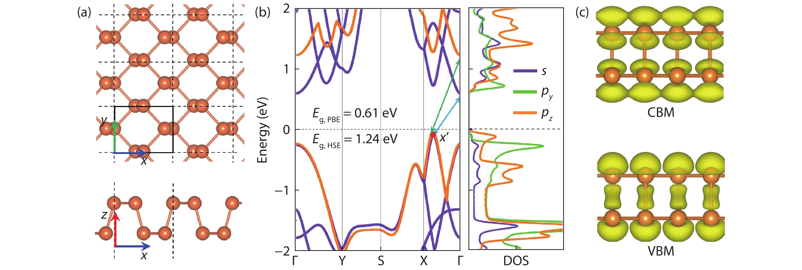
The optimized puckered arsenene belongs to orthorhombic system with lattice parameters of x = 4.73 Å, y = 3.68 Å. As shown in Fig. 1(a), arsenene holds a similar configuration to black phosphorene with four atoms in each unit cell, and each As atom is connected to other neighboring three ones exhibiting a puckered honeycomb structure. This honeycomb structure appears as an armchair and a zigzag edge along the x and y directions, respectively.
![]()
Figure 1.(Color online) (a) The top and side views of puckered arsenene. (b) The band structure at PBE (purple line) and HSE06 (orange line) level and the orbital-projected density of states of the puckered arsenene. (c) The partial charge density of CBM and VBM.
The simulated band structure of puckered arsenene at PBE level (the purple line) is shown in Fig. 1(b). The conduction band maximum (CBM) is located at Γ point, while the valence band minimum (VBM) occurs at the X’ point (between Γ and X points), leading to an indirect band gap of 0.61 eV. Since the PBE level usually underestimates the band gap, we then use the hybrid functional (HSE06) to provide a more accurate assessment with the value of 1.24 eV. To better understand the properties of the band edge, the orbital-projected density of states (DOS) and the wavefunctions of CBM and VBM (Fig. 1(c)) are also given, which shows that the CBM is comprised by the hybrid states of s-, py- and pz-orbitals, while the VBM is mainly distributed by the pz-states.
We calculate the effective mass of the band edge, which plays an important role in affecting the carrier mobility and transport performances of the FETs. The band dispersions of the CBM and VBM along armchair and zigzag directions are displayed in Fig. 2. As shown in Figs. 2(a) and 2(b), the band dispersions of electrons along armchair and zigzag directions hold a strong anisotropic characteristic, as the m* of electron (me*) in the zigzag direction is about four times larger than that in the armchair direction, that is 1.26m0 versus 0.35m0. The band dispersion of holes in these two directions are shown in Figs. 2(c) and 2(d), which also shows a little anisotropy. The m* of hole (mh*) in the armchair direction is 0.16m0, while that in the zigzag direction is 0.32m0.
![]()
Figure 2.(Color online) The band dispersions of the CBM along (a) the armchair direction and (b) the zigzag direction, and that of VBM along (c) the armchair direction and (d) the zigzag direction. The corresponding effective mass and carrier mobility are also marked out.
The carrier mobility is one of the most important figures of merits of the material properties toward the realization of an electronic device using puckered arsenene as channel. Here, we provide a qualitative estimation of the carrier mobility by using the deformation potential theory only considering the scatterings of longitudinal acoustic (LA) phonons. Although some other scattering mechanisms such as the acoustic flexural modes (ZA) and optical phonons may also have a strong suppression for the mobility, in MOSFET configurations, the dielectric oxide substrate and gate electrode will suppress the impact of ZA phonons largely and the effect of the optical phonons slightly on the mobility[
On the basis of the Takagi formula, except for the effective mass, another two parameters that play important roles in the mobility are the elastic moduli C2D and the deformation potential constant El. The values of C2D in the armchair and zigzag directions are 83.4 and 27.8 N/m, respectively. The values of El for electron and hole are anisotropic. Especially for the electrons, the El is 0.6 eV in the armchair direction, while it is 3.1 eV in the zigzag direction. For the holes, the values of E1 along armchair and zigzag directions are 9.3 eV and 2.6 eV, respectively. As a result, due to the ultra-small E1 and me*, the electron mobility (μe*) in the armchair direction presents an ultra-high value of 20 045 cm2V–1s–1, while that in the zigzag direction is 233 cm2V–1s–1. On the other hand, even though the hole along armchair holds a smaller m* than that of zigzag, the larger E1 severely weaken the hole mobility (μh*) and the value of μh* is 182 cm2V–1s–1, while that in the zigzag direction is 435 cm2V–1s–1.
Moreover, it should be noted that except for the coupling with ZA modes and the optical phonons, Takagi formula also neglects the anisotropy of the deformation potential matrix and the inter-valley scatterings. Thereby, the mobility we predicted here should be regarded as the most ideal situation. If a more accurate mobility closer to the experiments is needed, a full ab initio approach should be used[
We next present a device simulation based on double-gated MOSFETs. The device models with both armchair and zigzag orientations are selected as the transport directions and are shown in Figs. 3(a) and 3(c), respectively. The intrinsic puckered arsenene as the channel material located between the top and bottom SiO2 dielectric slabs. The thickness of the SiO2 is 0.5 nm and the permittivity is 3.9. The source and drain electrodes are highly doped with doping concentration of 3 × 1013 cm–2 for both n- and p-type MOSFETs.
![]()
Figure 3.(Color online) The schematic model of dual-gated puckered arsenene MOSFET along (a) the armchair and (c) zigzag direction. The transfer characteristics for puckered arsenene n- and p-MOSFETs along (b) the armchair and (d) zigzag direction with
To evaluate the potential logic applications of puckered arsenene FETs, we first investigate the transfer characteristics as a function of Lch. The supply voltage Vdd is 0.6 V according to the IRDS requirements for 2031 horizons[
The switching characteristic is one of the most important parameters to measure the performance of FETs, which can be clearly described by SS and on/off ratio. SS is defined as SS = (∂ lgIds/∂ Vgs)–1, which represents the amount of change in the gate voltage as the source-drain current changes by one order of magnitude at the sub-threshold region. A small SS usually means a fast switching speed. The on/off ratio is defined as ratio of on-current (Ion) and off-current (Ioff). The Ioff is 10 nA/μm according to the IRDS requirements for HP applications, while the Ion is ensured by the equation |Vgs, on – Vgs, off| = Vdd, where Vgs, on and Vgs, off are the gate–source voltage corresponding to the Ion and Ioff. The SS and the on/off ratio of the puckered arsenene MOSFETs are summarized in Fig. 4. As shown in Fig. 4(a), the SS of all the 10-nm-Lch puckered arsenene MOSFETs is smaller than the IRDS HP requirement of 75 mV/dec, in which the zigzag-directed p-FETs possess the smallest value of 65 mV/dec. As shown in Fig. 4(b), the on/off ratio of other three conditions with 10-nm-Lch except the zigzag-directed n-FET can all fulfill the requirements of the IRDS HP applications in 2031 horizons. This is because the heavier me* in the zigzag direction results in a low drain-source current. Furthermore, as the Lch decreases to 7 nm, although the SS appears a serious degradation, the on/off ratio of the zigzag-directed p-MOSFET can still reach the HP standard.
![]()
Figure 4.(Color online) The SS and the on/off ratio as a function of the
To reveal the operational principles of the MOSFETs along two different directions, the position resolved local density of states (LDOS) and the spectrum current of 5-nm-Lch n-MOSFETs at Vgs = –1 V and 5-nm-Lch p-MOSFETs at Vgs = 0.9 V are shown in Fig. 5. As shown in Fig. 5(a), a barrier height ΦB of 0.18 eV is generated for armchair-directed n-MOSFETs as Vgs = –1 V, so that the drain–source current is reduced to 0.8 μA/μm, while the position resolved LDOS of zigzag-directed n-MOSFETs in Fig. 5(b) shows that the Vgs of –1 V leads to a higher ΦB of 0.23 eV, and thereby the drain–source current of the zigzag-directed n-MOSFET decreases to a lower value of 0.02 μA/μm. Except for the difference of the ΦB, the m* is the other important parameter that plays an important role in leakage current. The larger the m*, the smaller the tunneling probability. Therefore, as shown in the spectrum current in Figs. 5(a) and 5(b), the armchair-directed n-MOSFET exhibits a larger specific tunneling current than zigzag-directed n-MOSFET at Vgs = –1 V. The anisotropy of the mh* is not as significant as that of me*, and thereby the proportion of tunneling current in the p-MOSFETs along two different orientations at Vgs = 0.9 V has no obvious difference, as shown in spectrum current of Figs. 5(c) and 5(d). For the p-MOSFET, the main reason why the zigzag-directed exhibits a smaller leakage current is the higher ΦB than the armchair-directed, which is 0.29 versus 0.13 eV.
![]()
Figure 5.(Color online) The position resolved LDOS and spectral currents of puckered arsenene n-FETs with 5-nm
The intrinsic delay time τ and power dissipation (PDP) are two essential figures of merit ultimately used to evaluate the switching speed and power consumption of FETs. The intrinsic delay time τ and the PDP per width of the puckered arsenene can be calculated by the equation
Furthermore, we assess the performances of 32-bit ALU circuits based on puckered arsenene FETs considering the interconnects and parasitic capacitances through the software BCB 3.0[
![]()
Figure 6.(Color online) Switching energy versus delay time,
4. Conclusion
In summary, we have comprehensively investigated the electronic properties and ballistic quantum transport properties of puckered arsenene using the DFT coupled with NEGF formalism. The puckered arsenene holds an ultra-high carrier mobility with the highest value reaching 20 045 cm2V–1s–1. In the 10-nm node, the puckered arsenene FETs possess a high on/off ratio above 105 and a steep SS below 75 mV/dec, which is suitable for HP applications. We also provide a benchmark for the intrinsic puckered arsenene FETs, showing that the zigzag-directed arsenene FETs possess faster switching speeds and low power dissipation. Moreover, the 32-bit ALU circuits simulation results also demonstrate that the arsenene FETs hold promising device performance and are comparable to CMOS technology and some other CMOS alternatives. Therefore, puckered arsenene broadens a promising way in the quest for the novel material that could replace silicon electronics.
Acknowledgements
This work was financially supported by the Training Program of the Major Research Plan of the National Natural Science Foundation of China (91964103), the Natural Science Foundation of Jiangsu Province (BK20180071), the Fundamental Research Funds for the Central Universities (No. 30919011109), and also sponsored by Qing Lan Project of Jiangsu Province, and the Six Talent Peaks Project of Jiangsu Province (Grant No. XCL-035).
References
[1] R Chau, B Doyle, S Datta et al. Integrated nanoelectronics for the future. Nat Mater, 6, 810(2007).
[2] A D Franklin. Nanomaterials in transistors: From high-performance to thin-film applications. Science, 349, aab2750(2015).
[3] S B Desai, S R Madhvapathy, A B Sachid et al. MoS2 transistors with 1-nanometer gate lengths. Science, 354, 99(2016).
[4] S L Zhang, S Y Guo, Z F Chen et al. Recent progress in 2D group-VA semiconductors: From theory to experiment. Chem Soc Rev, 47, 982(2018).
[5] S Y Guo, Y P Zhang, Y Q Ge et al. 2D V-V binary materials: Status and challenges. Adv Mater, 31, 1902352(2019).
[6] W H Zhou, S L Zhang, S Y Guo et al. Designing sub-10-nm metal-oxide-semiconductor field-effect transistors via ballistic transport and disparate effective mass: The case of two-dimensional BiN. Phys Rev Appl, 13, 044066(2020).
[7] W Cao, J H Kang, D Sarkar et al. 2D semiconductor FETs: Projections and design for sub-10 nm VLSI. IEEE Trans Electron Devices, 62, 3459(2015).
[8] Z L Zhu, X L Cai, S Yi et al. Multivalency-driven formation of Te-based monolayer materials: A combined first-principles and experimental study. Phys Rev Lett, 119, 106101(2017).
[9] Z Q Zhou, Y Cui, P H Tan et al. Optical and electrical properties of two-dimensional anisotropic materials. J Semicond, 40, 061001(2019).
[10] W H Zhou, J Y Chen, P X Bai et al. Two-dimensional pnictogen for field-effect transistors. Res Wash D C, 2019, 1046329(2019).
[11] K S Novoselov, A Mishchenko, A Carvalho et al. 2D materials and van der Waals heterostructures. Science, 353, aac9439(2016).
[12] S X Wang, Z H Yu, X R Wang. Electrical contacts to two-dimensional transition-metal dichalcogenides. J Semicond, 39, 124001(2018).
[13] F Schwierz. Graphene transistors. Nat Nanotechnol, 5, 487(2010).
[14] L Tao, E Cinquanta, D Chiappe et al. Silicene field-effect transistors operating at room temperature. Nat Nanotechnol, 10, 227(2015).
[15] A Nourbakhsh, A Zubair, R N Sajjad et al. MoS2 field-effect transistor with sub-10 nm channel length. Nano Lett, 16, 7798(2016).
[16] J S Qiao, X H Kong, Z X Hu et al. High-mobility transport anisotropy and linear dichroism in few-layer black phosphorus. Nat Commun, 5, 4475(2014).
[17] S L Zhang, Z Yan, Y F Li et al. Atomically thin arsenene and antimonene: Semimetal –semiconductor and indirect-direct band-gap transitions. Angew Chem Int Ed, 54, 3112(2015).
[18] L K Li, Y J Yu, G J Ye et al. Black phosphorus field-effect transistors. Nat Nanotechnol, 9, 372(2014).
[19] X X Wang, Y Hu, J B Mo et al. Arsenene: A potential therapeutic agent for acute promyelocytic leukaemia cells by acting on nuclear proteins. Angew Chem Int Ed, 59, 5151(2020).
[20] M Z Zhong, Q L Xia, L F Pan et al. Thickness-dependent carrier transport characteristics of a new 2D elemental semiconductor: Black arsenic. Adv Funct Mater, 28, 1802581(2018).
[21] X Wu, Y Shao, H Liu et al. Epitaxial growth and air-stability of monolayer antimonene on PdTe2. Adv Mater, 29, 1605407(2017).
[22] Y B Chen, C Y Chen, R Kealhofer et al. Black arsenic: A layered semiconductor with extreme in-plane anisotropy. Adv Mater, 30, 1800754(2018).
[23] G Pizzi, M Gibertini, E Dib et al. Performance of arsenene and antimonene double-gate MOSFETs from first principles. Nat Commun, 7, 12585(2016).
[24] R G Quhe, Q H Li, Q X Zhang et al. Simulations of quantum transport in sub-5-nm monolayer phosphorene transistors. Phys Rev Appl, 10, 024022(2018).
[25] J Wang, Q Cai, J M Lei et al. Performance of monolayer blue phosphorene double-gate MOSFETs from the first principles. ACS Appl Mater Interfaces, 11, 20956(2019).
[26] Y Y Wang, P Huang, M Ye et al. Many-body effect, carrier mobility, and device performance of hexagonal arsenene and antimonene. Chem Mater, 29, 2191(2017).
[27] G Kresse, J Furthmüller. Efficient iterative schemes forab initiototal-energy calculations using a plane-wave basis set. Phys Rev B, 54, 11169(1996).
[28] J P Perdew, K Burke, M Ernzerhof. Generalized gradient approximation made simple. Phys Rev Lett, 77, 3865(1996).
[29] S Grimme, S Ehrlich, L Goerigk. Effect of the damping function in dispersion corrected density functional theory. J Comput Chem, 32, 1456(2011).
[30] S Takagi, A Toriumi, M Iwase et al. On the universality of inversion layer mobility in Si MOSFET's: Part II-effects of surface orientation. IEEE Trans Electron Devices, 41, 2363(1994).
[31]
[32]
[33] G Gaddemane, W G Vandenberghe, M L van de Put et al. Theoretical studies of electronic transport in monolayer and bilayer phosphorene: A critical overview. Phys Rev B, 98, 115416(2018).
[34] S Poncé, E R Margine, F Giustino. Towards predictive many-body calculations of phonon-limited carrier mobilities in semiconductors. Phys Rev B, 97, 121201(2018).
[35]
[36] D E Nikonov, I A Young. Overview of beyond-CMOS devices and a uniform methodology for their benchmarking. Proc IEEE, 101, 2498(2013).
[37] D E Nikonov, I A Young. Benchmarking of beyond-CMOS exploratory devices for logic integrated circuits. IEEE J Explor Solid-State Comput Devices Circuits, 1, 3(2015).

Set citation alerts for the article
Please enter your email address
© Copyright 2018-2021 | Chinese Laser Press. All Rights Reserved 沪ICP备15018463号-20