
Chao Shen, Wenkang Zhan, Manyang Li, Zhenyu Sun, Jian Tang, Zhaofeng Wu, Chi Xu, Bo Xu, Chao Zhao, Zhanguo Wang. Development of in situ characterization techniques in molecular beam epitaxy[J]. Journal of Semiconductors, 2024, 45(3): 031301
- Journal of Semiconductors
- Vol. 45, Issue 3, 031301 (2024)
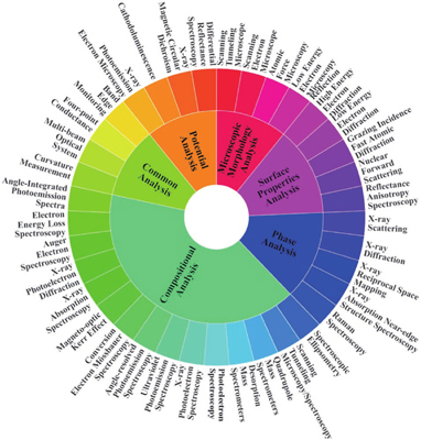
Fig. 1. (Color online) In situ characterization techniques applied in MBE.
![(Color online) STM images of filled states obtained after sequential depositions at 500 °C: (a) 0.6 ML ErSb on a GaSb (001) surface, followed by (b) 2 ML of GaSb, and then followed by (c) an additional 0.6 ML ErSb. STM images acquired after depositing additional GaSb on the surface shown in (a). (d) 4 ML of GaSb and (e) 10 ML of GaSb. Higher-resolution STM insets (10 nm × 10 nm) reveal the surface reconstruction of the ErSb sites, with (a–c) showing exposed ErSb and (d-e) showing GaSb coverage over the ErSb sites. Reproduced with permission. Ref. [44] Copyright 2013, American Chemical Society.](/richHtml/jos/2024/45/3/031301/jos_45_3_031301_f2.jpg)
Fig. 2. (Color online) STM images of filled states obtained after sequential depositions at 500 °C: (a) 0.6 ML ErSb on a GaSb (001) surface, followed by (b) 2 ML of GaSb, and then followed by (c) an additional 0.6 ML ErSb. STM images acquired after depositing additional GaSb on the surface shown in (a). (d) 4 ML of GaSb and (e) 10 ML of GaSb. Higher-resolution STM insets (10 nm × 10 nm) reveal the surface reconstruction of the ErSb sites, with (a–c) showing exposed ErSb and (d-e) showing GaSb coverage over the ErSb sites. Reproduced with permission. Ref. [44] Copyright 2013, American Chemical Society.
Fig. 3. (Color online) (a) STM image of the modulated honeycomb
Fig. 4. (Color online) STM image of c(6 × 12) reconstructions on wurtzite GaN(
Fig. 5. (Color online) In situ AFM images for as-grown NiO on Ni(110) in (a) air, (b) water, and (c) 10 mM Pb-contained solution for 15 h. MBE-grown NiO on MgO(001) in (d) air, (e) water, and (f) 10 mM Pb-contained solution for 15 h. Reproduced with permission. Ref. [58].
Fig. 6. SnS on graphene substrates as a function of temperature as observed by LEEM. Reproduced with permission. Ref. [60] Copyright 2018, American Chemical Society.
Fig. 7. (Color online) RHEED patterns taken after the growth of (a) CaTi5O11 and (b) TiO2-B films on (001) SrTiO3 substrates. Reproduced with permission. Ref. [66].
Fig. 8. (Color online) RHEED patterns, corresponding STM images, and modeled patterns of GaN films deposited with different I/A ratios. Reproduced with permission. Ref. [54].
Fig. 9. (Color online) RHEED patterns of Fe1−xZnx films deposited on MgO (001) substrates: (a) and (b) pure Fe, (c) and (d) low Zn concentration, (e) and (f) moderate Zn concentration with α to Γ phase transition and (g) and (h) Fe0.29Zn0.71 with Γ phase. Reproduced with permission. Ref. [81] Copyright 2011, AIP Publishing.
Fig. 10. (Color online) (a) RHEED images of the SrTiO3(001) substrate. RHHED images of the SrCoO2.5 grown on substrate with different Co/Sr ratios: (b) Co/Sr = 1.00, (c) Co/Sr = 1.30, and (d) Co/Sr = 0.90. Reproduced with permission. Ref. [88].
Fig. 11. REELS spectra, RHEED patterns, and AFM images of AlN: (a) a smooth surface, (b) a rougher surface. Reproduced with permission. Ref. [70] Copyright 2011, AIP Publishing.
Fig. 12. Evolution of LEED patterns of coronene monolayers on Cu(110) surface during (A−G) the heating and (H) cooling process. Reproduced with permission. Ref. [102] Copyright 2010, American Chemical Society.
Fig. 13. (Color online) Typical LEED patterns of the silicene-stanene on Ag(111) during hetero-epitaxy. (a) Post preparation at incident energy. (b) After Si deposition. (c) After Sn deposition. (d) After non-reactive Al2O3 encapsulation. Reproduced with permission. Ref. [105].
Fig. 14. (Color online) Specular rod for LSAT(001) measured with X-rays and calculated profiles. (a) Calculated rod for AO-terminated LSAT Substrates with varying La0.18Sr0.82O surface coverage. (b) Calculated rod with varying topmost plane displacement relative to the bulk LSAT lattice parameter at growth temperature. (c) Calculated rod accounting for both surface coverage and surface relaxation. Reproduced with permission. Ref. [117].
Fig. 15. (Color online) Selected XRD spectra of the sub-free SDD-GaSe film during pressurization. Reproduced with permission. Ref. [127].
Fig. 16. (Color online) Diffraction intensity as a function of time, in nanowires annealed at 610 °C. Reproduced with permission. Ref. [130] Copyright 2019, American Chemical Society.
Fig. 17. (Color online) Results of the in situ XANES measurements. (a) The single-phase brownmillerite-structured SrCoO2.5. (b) Two-phase brownmillerite-structured SrCoO2.5 and Sr3Co2O6±δ films. Reproduced with permission. Ref. [119] Copyright 2018, American Chemical Society.
Fig. 18. (Color online) Layer-dependent STS reveals the transition from semiconductor to semimetal as the layer number increases from one to six in PtSe2 on highly oriented pyrolytic graphite (HOPG). Reproduced with permission. Ref. [147] Copyright 2021, Wiley-VCH GmbH.
Fig. 19. (Color online) Desorption during the growth of InxGa1–xN/GaN nanowires by MBE. (a) Calibration of full desorption and background pressure at 800 °C, with the growth of a segment at 604 °C. (b) Comparison of InxGa1–xN quantum well (QW) (blue line) and extended NW segment (red line) growth at the same temperature. (c) In desorption during InxGa1–xN QW growth at different substrate temperatures. Reproduced with permission. Ref. [151] Copyright 2012, American Chemical Society.
Fig. 20. (Color online) (a) Valence band maximum measured by UPS for Cu2O with nominal thickness of 42 nm. (b) Core-level energy spectrum measured by XPS for Cu2O with nominal thickness of 42 nm. Reproduced with permission. Ref. [162].
Fig. 21. (Color online) A series of ARPES spectra of YbAl3 was collected along the (0, 0) to (0, π) direction at kz ≈ Γ, spanning temperatures from 255 down to 21 K. Reproduced with permission. Ref. [168].
Fig. 22. (Color online) (a) Angle-integrated photoemission spectroscopy (PES) of various SIO−STO SLs and the SIO-214 film. The dotted black line represents the Fermi energy (EF), while the blue (orange) shaded region corresponds to the peak position of the Jeff = 1/2 (Jeff = 3/2) bands. (b) Schematic model illustrating the bandwidth-control Mott transition in SIO−STO SLs and the SIO-214 film. Reproduced with permission. Ref. [184].
Fig. 23. (Color online) (a) In situ reflectivity profiles of samples B to E, exhibiting significant variations in GR and N/In ratio. (b) The extracted 1 st reflectivity profiles of samples B to E during (
Fig. 24. (Color online) Statistics of in situ characterization techniques involved in publications in recent years.
|
Table 1. A summary of the advantages, disadvantages, and functions of characterization technologies.

Set citation alerts for the article
Please enter your email address
© Copyright 2018-2021 | Chinese Laser Press. All Rights Reserved 沪ICP备15018463号-20