Abstract
Ex situ characterization techniques in molecular beam epitaxy (MBE) have inherent limitations, such as being prone to sample contamination and unstable surfaces during sample transfer from the MBE chamber. In recent years, the need for improved accuracy and reliability in measurement has driven the increasing adoption of in situ characterization techniques. These techniques, such as reflection high-energy electron diffraction, scanning tunneling microscopy, and X-ray photoelectron spectroscopy, allow direct observation of film growth processes in real time without exposing the sample to air, hence offering insights into the growth mechanisms of epitaxial films with controlled properties. By combining multiple in situ characterization techniques with MBE, researchers can better understand film growth processes, realizing novel materials with customized properties and extensive applications. This review aims to overview the benefits and achievements of in situ characterization techniques in MBE and their applications for material science research. In addition, through further analysis of these techniques regarding their challenges and potential solutions, particularly highlighting the assistance of machine learning to correlate in situ characterization with other material information, we hope to provide a guideline for future efforts in the development of novel monitoring and control schemes for MBE growth processes with improved material properties.Introduction
Molecular beam epitaxy (MBE) is a versatile and powerful technique that has revolutionized material synthesis and design. It allows researchers to engineer materials with tailored properties for applications in diverse fields, such as photonics, energy conversion, and catalysis, by providing a high degree of control over the composition, structure, and properties of the films[1−5]. During MBE growth, the substrate and evaporation sources can be regulated, allowing for the generation of atomic or molecular beams that travel nearly straight towards the substrate surface. These beams are slowly deposited on the heated substrate, forming highly crystalline and atomically smooth thin-film layers[6, 7]. Compared with traditional film growth methods, MBE enables atomic-scale control and offers several key advantages, such as the ability to grow at relatively low temperatures, precise control over parameters, and an ultra-high vacuum environment, facilitating the production of large-area materials with minimal defects and outstanding performance[8−12]. MBE also provides a platform for systematic studies of the structure-property relationship in materials, laying the foundation for the development of materials for various applications[13−16].
There are, however, several outstanding issues that have not been adequately addressed in MBE. On the one hand, many related factors interact to determine the growth quality and even a tiny deviation can lead to the formation of various defects[17, 18]. As an example, the growth temperature plays a crucial role in regulating the atoms' adhesion coefficient, adsorption, and desorption capabilities. To improve growth quality, high-temperature growth is utilized to effectively reduce bulk defects and unwanted impurities by promoting step-flow growth. However, the excessive temperature variation introduced in the growth process can also have a negative impact on the film quality[19−22]. Therefore, it is necessary to find the optimal balance between different parameters. On the other hand, the instability of material growth environment can also cause other unknown effects. For instance, the traditional thermocouple-based temperature monitoring, which typically has a significant deviation from the actual temperatures, cannot ensure excellent stability for temperature control, thus increasing the difficulties for optimizing the growth parameters[19, 23−25].
Advanced characterization technologies, such as X-ray diffraction (XRD), Raman spectroscopy (RS), and photoelectron spectroscopy (PES), have been incorporated into MBE to gain insight into material growth mechanisms and optimizing growth parameters. These characterization techniques can be classified into two categories: ex situ and in situ, in which choosing suitable characterization techniques plays a crucial role in improving material quality[26−28]. Although ex Received 7 JULY 2023; Revised 5 AUGUST 2023. Characterization is currently predominantly employed, it has several inherent limitations. For instance, ex situ characterization normally requires transferring the sample from the MBE chamber, resulting in the exposure of the thin films to the atmosphere, the formation of an oxide layer, and the contamination of surface, thereby compromising the characterization results and leading to incorrect guidelines about the material growth conditions. Therefore, the information provided by ex situ characterization may not accurately reflect the true structure and properties of the material in its original environment[29−31]. Additionally, traditional ex situ measurement methods may leave surface imprints, which can be challenging to remove, degrading the surface quality. As an example, the research on the instability of bismuth (Bi) on substrate surfaces in V-rich environments has shown that ex situ characterization techniques may yield inaccurate results due to changes of the vacuum environment, while in situ characterization can effectively address these challenges by preserving the vacuum conditions[32].
Thus, with careful consideration to minimize the environmental impact on the samples during characterization, in situ characterization techniques have been widely applied, offering a range of capabilities beyond those of ex situ characterization[32]. In situ characterization allows for accurate material characterization in their original environment, tracking dynamic material changes in structure, morphology, and reaction kinetics, and providing rapid characterization results, typically in real time[25]. By enabling in situ monitoring of the material and subsequent characterization without exposing the sample to air, in situ techniques can eliminate unwanted stoichiometry impacts, ensuring that films are not subjected to active contaminants present during ex situ characterization[33, 34]. Although most contaminants can be removed by moderate heating, ex situ characterization equipment often lacks such heating capabilities. Moreover, in addition to avoiding issues caused by sample transfer, in situ characterization is typically nondestructive, which is highly desired in material studies[35−38]. Therefore, in situ characterization techniques hold significant importance in the field of MBE. However, only a few reviews of this topic have been published, either focusing on specific applications, such as sodium-ion batteries, or merely covering a number of selected characterization techniques[39−41]. Thus, a thorough review of these in situ characterization techniques can contribute to a better understanding of materials growth principles, methodologies, and applications, enabling researchers to make informed choices in selecting the most suitable techniques for specific material systems.
This review is organized as follows. In Section 2, numerous in situ characterization techniques are categorized, based on their functionalities and the information to be extracted, into microscopic morphology analysis in Section 2.1, surface properties analysis in Section 2.2, phase analysis in Section 2.3, composition analysis in Section 2.4 and common analysis in Section 2.5. In addition, their applications and advantages are summarized. In Section 2.6, several promising techniques with great potential for future integration with MBE are illustrated. In Section 3, we discussed the limitations of the existing in situ characterization techniques and point to some potential routes for future development. Finally, our conclusions are presented in Section 4.
In situ characterization techniques in MBE
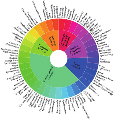
In situ characterization techniques applied in MBE are reviewed in this section. It is important to note that these characterization techniques, some of which can be utilized for multiple purposes, have been categorized according to their primary use into the following categories: microscopic morphology analysis, surface properties analysis, phase analysis, compositional analysis, and common analysis. We summarize the applications of these in situ characterization techniques and evaluate their advantages and disadvantages. The techniques included in this review are displayed in Fig. 1, in which we also listed the potential analysis to be integrated with MBE in the future.

Figure 1.(Color online) In situ characterization techniques applied in MBE.
Microscopic morphology analysis
Microscopic techniques, such as scanning tunneling microscopy (STM), scanning electron microscopes (SEM), atomic force microscopy (AFM), and low-energy electron microscopy (LEEM), can provide a wealth of microscopic surface information. These techniques also enable researchers to gain insight into the evolution of the growth by observing surface changes in materials, with several of them having been integrated with MBE.
Scanning tunneling microscopy (STM)
In situ STM has been used to analyze nucleation and growth kinetics in the early stages of growth. For example, Socha et al. observed the island-like growth pattern of the film through STM and directly determined the correlation between the STM image and the film surface height[42]. Similarly, Yang et al. used STM to characterize GaN with increasing thickness, discovering that due to different growth gradients throughout the film, a three-dimensional growth mode of GaN in both horizontal and vertical directions was achieved with MBE, which was potentially originated from thread dislocations or strain relaxation during growth[43]. Kawasaki et al. found that the ErSb/GaSb nanostructures formed via a surface-mediated self-assembly mechanism, through the observation by STM during growth, as shown in Fig. 2[44]. They explained that the growth occurs entirely during the initial stages and is not a result of diffusion or segregation. Additionally, when studying the growth of graphene on Au(111) surface, Hernández et al. found dendritic islands accumulated at the edge of the atomic step with STM[45]. Haze et al. obtained the local electronic structure around non-magnetic Zn impurities in CeCoIn5 film by combining STM with MBE, providing a convenient way to study the electronic properties of heavy fermion compounds[46]. These studies demonstrated the power of in situ STM in providing valuable insight into the growth process of semiconductor materials and its potential for optimizing growth parameters.
Figure 2.(Color online) STM images of filled states obtained after sequential depositions at 500 °C: (a) 0.6 ML ErSb on a GaSb (001) surface, followed by (b) 2 ML of GaSb, and then followed by (c) an additional 0.6 ML ErSb. STM images acquired after depositing additional GaSb on the surface shown in (a). (d) 4 ML of GaSb and (e) 10 ML of GaSb. Higher-resolution STM insets (10 nm × 10 nm) reveal the surface reconstruction of the ErSb sites, with (a–c) showing exposed ErSb and (d-e) showing GaSb coverage over the ErSb sites. Reproduced with permission. Ref. [44] Copyright 2013, American Chemical Society.
For the exploration of new materials, Zhang et al. leveraged the power of in situ characterization techniques, combining low-temperature STM and low-energy electron diffraction (LEED), to obtain a phosphorene structure model on Au(111) surface[27]. This structure was highly consistent with the calculation results of density functional theory (DFT). Cai et al. used STM and ex situ X-ray photoelectron spectroscopy (XPS) valence analysis results to prove the successful growth of CeOI thin films[47]. Similarly, Dávila et al. synthesized germanene layers on Au(111) and identified the material by combining STM and LEED observations with DFT calculations, as shown in Fig. 3[48]. These studies demonstrate the importance and capability of in situ characterization techniques of STM in developing and understanding new materials.
Figure 3.(Color online) (a) STM image of the modulated honeycomb × superstructure with a close-up in the bottom left corner. (b) The LEED pattern of (a). (c) Schematic representation of one-sixth of the pattern, where filled dots represent the hidden (0, 0) spot and integer-order spots, and open circles represent spots corresponding to the × superstructure (in red), the × superstructure (in green), and the 5 × 5 superstructure (in blue). Reproduced with permission. Ref. [48].
Combining in situ STM with other characterization techniques offers a powerful tool for understanding the growth mechanisms and optimizing the quality of materials[49]. Using spectroscopic imaging and STM, Wu et al. successfully revealed different energy scales of the local state's density and explained the origins of pseudo gap and superconductivity[50]. By combining STM, reflection high energy electron diffraction (RHEED), and angle-resolved photoelectron spectroscopy (ARPES), Song et al. were able to identify new materials and reveal their properties with atomic-plane resolution[51]. They determined the optimum temperatures for layer-by-layer growth of Bi2Se3 films in Se-rich conditions. When the growth thickness exceeded 10 atomic layers, they also found that the film became a bulk insulator. Lin et al. combined low-temperature superconducting magnets spin-polarized STM with MBE, which allows for high-quality data collection without compromising the vacuum integrity, as shown in Fig. 4, illustrating the reconstructions of GaN[38].
Figure 4.(Color online) STM image of c(6 × 12) reconstructions on wurtzite GaN(). Reproduced with permission. Ref. [38] Copyright 2014, AIP Publishing.
Much emphasis has been placed on the development of self-assembled quantum dots in recent years. However, the lack of understanding of the precise mechanism of quantum dot self-assembly hampers the effective control of their size, density, and distribution for specific applications. With the development of in situ techniques such as STM, researchers have overcome these challenges and achieved highly crystalline quantum dots. Toujyou et al. applied a voltage to the tip at a specific position on the two-dimensional wetting layer during growth and simultaneously observed it through in situ STM, leveraging the mechanism that the nucleation of quantum dots can be affected by tiny alloy fluctuations of the two-dimensional wetting layer, thus successfully realizing the fabrication of site-controlled and high-crystalline InAs quantum dots[52, 53]. Similarly, Rauschenbach et al. used in situ RHEED and STM to study the factors that affect the crystalline quality of GaN film, finding that the ratio of ions to atoms is the key to control the thin-film's growth mode[54]. They grew two-dimensional thin films of GaN with smooth morphology, high crystalline quality, low biaxial stress, and low defect density by controlling this ratio.
Scanning electron microscopes (SEM)
SEM offers enhanced observation of discernible phenomena during MBE processes, by providing an expansive field of view. For instance, SEM provides better performance, compared to STM with a more limited observation field, when adatom diffusion lengths become significant during high-temperature growth. Homma et al. have used SEM to study the effects of changes in adatoms at the kink points of atomic steps during crystal growth[55]. SEM can also observe the growth process, including island growth, coalescence, and completion of monolayer growth. Furthermore, for the initial stages of nanowire growth in the presence of a catalyst, SEM can observe the dynamic changes in nanowire growth and provide insight into the growth mechanism, potentially including the dissolution of the substrate by the catalyst and the filling of nanowires by the catalyst[56]. Kolíbal et al. employed SEM to investigate the initial stage of surface nucleation in thin films, discovering that the primary factor causing growth delay in nanowires is the filling of droplets by nanowire materials[56]. Wang et al. used SEM to observe micro-scale indium (In) droplets, resulting in the discovery of in situ droplet formation[57].
Atomic force microscopy (AFM)
AFM, in combination with other characterization techniques, such as STM reviewed in the previous section, can provide valuable insight into growth process and material properties, and verify the roughness, structure and morphology of the film surface during growth. The non-contact AFM can also be used to get large-area images with atomic resolution and identify different reconstructions. For example, from in situ AFM results shown in Fig. 5, Kim et al. investigated the contribution of defects in the chemical reaction between a Pb-containing solution and an oxide surface, using as-grown NiO on Ni(110) as the sample with defect, and the MBE-grown NiO on MgO(001) substrate as the defect-free one[58]. Deng et al. utilized STM and AFM to investigate the growth of single-layer FeTe films on NbSe2 single crystals, discovering that the Moiré superlattice modulation undergoes structural relaxation at larger orientation deviation angles[59].
Figure 5.(Color online) In situ AFM images for as-grown NiO on Ni(110) in (a) air, (b) water, and (c) 10 mM Pb-contained solution for 15 h. MBE-grown NiO on MgO(001) in (d) air, (e) water, and (f) 10 mM Pb-contained solution for 15 h. Reproduced with permission. Ref. [58].
Low-energy electron microscopy (LEEM)
Compared with other characterization techniques, low-energy electron microscopy (LEEM) allows for real-time observation of sample changes in vacuum or with exposure to gases or vapors in variable temperature environments, even at ultra-high temperatures[60]. As an example shown in Fig. 6, LEEM can be utilized in a wide range of temperatures in MBE, from 135 to 316 °C. LEEM is mainly used in surface studies of materials. For instance, Fortin et al. used LEEM patterns to monitor the substrate passivation process, the formation of a chemically stable layer on material surface to protect it from the influence of impurity ions or elements, demonstrating that Ge passivation prior to epitaxy allows tuning the electronic properties of antimonene (2D-Sb)[61]. Kanjanachuchai et al. studied morphological changes in Ⅲ−Ⅴ heteroepitaxial thin films and used LEEM to observe the nucleation and kinetics of Ⅲ droplets[62]. Mandziak et al. optimized the growth parameters and Fe doping for NiO thin films deposited on Ru(0001) using LEED[63]. Croes et al. used LEEM to explore the volume fraction of ferroelectric domains and domain sizes across a wide range of film thicknesses, demonstrating that interfacial misfit dislocations formed during growth play a vital role in the stability of ferroelectric nanodomains[64].
Figure 6.SnS on graphene substrates as a function of temperature as observed by LEEM. Reproduced with permission. Ref. [60] Copyright 2018, American Chemical Society.
Surface properties analysis
Surface properties and microscopic morphology analysis are two distinct categories of characterization techniques that are commonly used to study the properties and behaviors of materials. One of the apparent differences between them is the time interval between each observation. On the one hand, microscopic morphology analysis primarily gathers data via point-by-point scanning and assembles it into a complete data map, which is a time-consuming process to fine-tune the device parameters in order to obtain high-quality data. On the other hand, surface property analysis focuses on utilizing electron beams or rays to acquire information about the material, typically acquiring data with a receiving device such as a fluorescent screen or a display. Hence, one of the critical benefits of surface property analysis is the capacity to swiftly and constantly obtain data, such as reciprocal lattice. It prevents missing the necessary phenomenon owing to parameter change and enables a deeper understanding of material surface structure and properties.
Reflection high energy electron diffraction (RHEED)
RHEED is a powerful in situ characterization technique that provides valuable insights into the surface properties of thin films through the analysis of reciprocal lattice rods[65]. This technique is widely employed in the semiconductor industry to monitor surface cleanliness, analyze reconstruction, evaluate surface flatness or roughness, determine crystalline quality, and measure lattice constant evolution and stress-strain changes[66−71]. For example, the presence of a suitable buffer layer and the absence of stress-strain changes can be determined by analyzing RHEED patterns, as shown in Fig. 7[66]. The presence of bright specular stripes at 1.5 × indicates a flat and phase-pure CaTi5O11 surface, while the TiO2-B membrane also exhibits distinct and unadulterated 1.5 × stripes. Additionally, recording and analyzing RHEED diffraction patterns enables the optimization of growth conditions of different materials and the realization of high-quality epitaxy[67, 72]. As shown in Fig. 8, the surface morphology of GaN films with a thickness of about 10 nm was obtained from STM, along with the corresponding final RHEED patterns. In the case of ion to atom ratio (I/A) = 3.1, the surface exhibits islands and the corresponding RHEED pattern consists of point reflections, which indicates a three-dimensional growth. In contrast, GaN films deposited with I/A = 1.6 show a relatively flat surface with wide terraces, and the RHEED pattern consists of narrow striped reflections, representing a typical two-dimensional growth mode. Moreover, Li et al. monitored the surface structure evolution of the of ZnO films during the growth process and found that all the grown films exhibited good crystallinity properties in the wurtzite phase with RHEED[73].
Figure 7.(Color online) RHEED patterns taken after the growth of (a) CaTi5O11 and (b) TiO2-B films on (001) SrTiO3 substrates. Reproduced with permission. Ref. [66].
Figure 8.(Color online) RHEED patterns, corresponding STM images, and modeled patterns of GaN films deposited with different I/A ratios. Reproduced with permission. Ref. [54].
Moreover, an RHEED pattern is a powerful tool for understanding the growth mechanism of thin films. For example, Li et al. demonstrated that Zn-polar ZnO films grow through the standard Stranski-Krastanov mode, while O-polar ZnO films grow through a layer−by−layer mechanism[74]. In addition, with RHEED analysis, Dau et al. reported a fascinating discovery regarding the growth of Ge nanowires on Si(111) surfaces[75]. Through careful investigation, the researchers identified an Au-wetting layer located between the Ge nanowires and the substrate. This layer acts as a surfactant, facilitating the growth of the Ge layer between the nanowires. In addition, RHEED is also essential for understanding the growth characteristics of superlattices, particularly the mismatch of lattice and strain driving forces[76]. By controlling growth parameters such as temperatures of substrate and source via RHEED, researchers like Mietze et al. have achieved perfect superlattice growth of metastable cubic GaN/AlN layers[77]. When the thickness ratio of the compressive and tensile layers is 3/4, Yang et al. optimized the superlattice structure to achieve complete strain relaxation with RHEED and XRD analyses[78].
Additionally, the real-time analytical capabilities of RHEED are widely regarded as its most valuable feature. By providing a wealth of information about the growth window of parameters and slight deviations caused by non-stoichiometry, RHEED offers unparalleled insights into the dynamics of thin-film growth[79, 80]. For instance, McClure et al. utilized in situ RHEED to study the crystal structure transition of α-Fe phase to Γ phase in Fe1−xZnx alloys, discovering that the transition mainly occurred at 40% Zn concentration, as shown in Fig. 9[81]. Halder et al. used in situ RHEED to precisely determine the timing of transitions from two-dimensional to three-dimensional growth of InAlGaAs quantum dot[82]. Zhao et al. successfully observed the transition from three-dimensional to two-dimensional growth process on the surface of the ZnTe epitaxial layer through RHEED, which lasted about one minute[83]. Additionally, Hu et al. employed in situ RHEED to study the growth modes of ZnTe layers and determined the relationship between the Ⅵ/Ⅱ ratio and the growth modes transition between two-dimensional and three-dimensional[84].
Figure 9.(Color online) RHEED patterns of Fe1−xZnx films deposited on MgO (001) substrates: (a) and (b) pure Fe, (c) and (d) low Zn concentration, (e) and (f) moderate Zn concentration with α to Γ phase transition and (g) and (h) Fe0.29Zn0.71 with Γ phase. Reproduced with permission. Ref. [81] Copyright 2011, AIP Publishing.
Real-time analysis is also beneficial for quantifying surface reconstruction and determining the optimal growth conditions for thin films. Studies have shown that monitoring the oscillation of RHEED intensity can accurately determine the number of monolayers in a film, as demonstrated by Encomendero et al[85]. Dursap et al. used RHEED to track the growth of wurtzite-phase GaAs nanowires in real time, achieving controlled growth of these critical materials for electronic and optoelectronic applications[86]. Li et al. revealed that the film structure varied with growth temperature and Mg/B ratio during the epitaxy of MgB2 thin films, using RHEED[87]. With the assistance of RHEED in the growth of GaN thin films on (0001)-oriented 6H-SiC substrates via nitrogen ion beam assisted MBE, Rauschenbach et al. found that the RHEED patterns changed along with different ion to atom (I/A) ratios and they successfully controlled the growth of island-like and flat-structured GaN, as shown in Fig 8[54]. Therefore, the in situ RHEED system enables real-time growth monitoring, making it a powerful tool for optimizing growth parameters to achieve specific film growth and better understanding of the surface growth mechanism.
RHEED also offers high detection sensitivity and compatibility in addition to its real-time analysis capabilities. Its ability to detect slight changes in composition, such as the excess or deficiency of cobalt (Co) in strontium cobaltite (SCO) thin films, as demonstrated by Schöffmann et al., allows for high-precision growth and rapid adjustment of growth parameters[88]. They found that the RHEED pattern is sensitive to the slight change of the Co amount, while XRD failed to reveal this difference. As shown in Fig. 10, two additional sets of spots appear in the RHEED diffraction pattern with Co/Sr = 1.30, indicating well-crystallized three-dimensional structures. Conversely, when the Co/Sr ratio is low, the RHEED pattern only shows very weak Bragg spots and rough Laue rings with Co/Sr = 0.90, indicating a decrease in crystallinity. Furthermore, RHEED can be combined with other characterization techniques, such as XRD, laser reflection, and glancing-angle reflectance electron energy loss spectroscopy, to provide a more comprehensive understanding of the material under study[89−91]. Taking advantages of the high sensitivity of laser reflection signals to species and surface morphology, and corresponding the significant decrease during In deposition and the increase during N irradiation in RHEED intensity with the opposite variation trend of laser reflection intensity, Wang et al. have demonstrated that the laser reflection signal can serve as a valuable complement to RHEED[57]. In addition, Strawbridge et al. also achieved in situ monitoring of the growth of Ⅲ-nitride thin films by combining RHEED, AFM with glancing-angle reflectance electron energy loss spectroscopy (REELS)[70]. As shown in Fig. 11, the RHEED patterns and AFM images are utilized to discern the surface roughness of films, thereby correlating smooth surfaces with a plasmon peak at 16.9 eV and rough surfaces with a peak at 21.4 eV in the REELS spectrum. Jakob et al. compared the potential applications of RHEED with XRD in MBE and highlighted the potential of combining these two techniques to translate time-resolved information into height-resolved information analysis, without the need for prior assumptions about growth modes, which are, in contrast, typically required by traditional methods[92]. Although the definitive study of RHEED focuses on the analysis of diffraction patterns, Sen et al. have shown that the use of diffuse scattering in RHEED can also qualitatively trace the variation of thin metallic layer thickness[93]. Besides monitoring, RHEED can also be used as a source of high-energy electrons to adjust surface status, or generate X-ray fluorescence for composition analysis. May et al. successfully obtained a GaAs seed layer on the surface of single crystals by utilizing a combination of careful RHEED beam exposure and methods to increase adatom mobility[94]. They demonstrated the effectiveness of this method in promoting GaAs nucleation on NaCl substrates. With the using of X-ray fluorescence generated from the RHEED measurements, Keenan et al. achieved in situ determination of the relative compositions of Y and Mn during YMnO3 growth on GaN template/sapphire substrate[95].
Figure 10.(Color online) (a) RHEED images of the SrTiO3(001) substrate. RHHED images of the SrCoO2.5 grown on substrate with different Co/Sr ratios: (b) Co/Sr = 1.00, (c) Co/Sr = 1.30, and (d) Co/Sr = 0.90. Reproduced with permission. Ref. [88].
Figure 11.REELS spectra, RHEED patterns, and AFM images of AlN: (a) a smooth surface, (b) a rougher surface. Reproduced with permission. Ref. [70] Copyright 2011, AIP Publishing.
Recent advances in machine learning techniques have further enhanced the capabilities of RHEED by automating the classification and analysis of diffraction patterns. By using principal component analysis and k-means clustering, Provence et al. showed that RHEED analysis with the assist of machine learning can help understand surface evolution during growth and provide more insight into the growth process of perovskite oxides[96]. Kwoen et al. identified feature points from the atlas input database and then used the trained model to classify the experimental data through machine learning, with which they achieved automatic classification and high classification accuracy of RHEED images of GaAs reconstructions[79]. With great significance in accomplishing high reproducibility for epitaxial growth, this technique sees a wide range of potential applications in the field of high-quality Ⅲ−Ⅴ growth. Recently, his team also realized the identification of RHEED patterns through unsupervised learning mechanisms[97]. Therefore, machine learning has proven to be a valuable tool in RHEED analysis, providing researchers with more efficient and accurate results.
Low-energy electron diffraction (LEED)
LEED is another of the most widely applied techniques for surface structure analysis, which differs with RHEED in the mode of electron incidence and path for scattered electrons. More specifically, RHEED uses grazing incidence and forward scattered electrons, while LEED employs normal incidence and backscattered electrons. By directing lower energy electrons onto a surface and measuring their diffraction pattern on a fluorescent screen, LEED can determine the surface structure of the sample and characterize crystallinity, surface relaxation, and the reconstruction of adsorbate-covered surfaces[84, 98−101]. Researchers, such as Zhang et al., have combined LEED patterns with density functional theory calculation to study the relationship between structural transitions and substrate temperature for depositing coronene monolayers on Cu(110) surfaces[102]. By calculating the temperature dependence of free energy, they explained the irreversible transition and the stable state determined by the LEED patterns shown in Fig. 12. Ruwisch et al. and Navío et al. achieved quality control of individual films and determined the chemical composition of the near-surface region and the surface structure of each layer by in situ XPS and LEED[103, 104].
Figure 12.Evolution of LEED patterns of coronene monolayers on Cu(110) surface during (A−G) the heating and (H) cooling process. Reproduced with permission. Ref. [102] Copyright 2010, American Chemical Society.
To solve the issue of realizing Xene (X = Si, Ge, Sn, etc.) heterostructures, Dhungana et al. introduced a concept based on epitaxy of silicene and stanene on Ag(111) and used LEED to monitor and identify the surface structure, as shown in Fig. 13[105]. The study demonstrated a feasible single Xene layer enabling another type of Xene layer with distinct properties produced heterogeneously subsequently. However, the use of electron guns and detectors in LEED requires them to be positioned near the substrate. As a result, surface probing during the deposition process is not supported[106].
Figure 13.(Color online) Typical LEED patterns of the silicene-stanene on Ag(111) during hetero-epitaxy. (a) Post preparation at incident energy. (b) After Si deposition. (c) After Sn deposition. (d) After non-reactive Al2O3 encapsulation. Reproduced with permission. Ref. [105].
Other surface properties analysis techniques
Additionally, several in situ surface characterization techniques have also been integrated into MBE, such as grazing-incidence fast atomic diffraction (GIFAD), nuclear norward scattering (NFS), and reflectance anisotropy spectroscopy (RAS). GIFAD, as a technique suitable for in situ measurement of complex surface reconstruction, has been rapidly developed. GIFAD obtains surface information by controlling factors such as the incidence angle and scattering angle of heavy ion beams introduced into the material surface. Its exceptional sensitivity to subtle surface changes makes it an ideal tool for high-resolution, real-time monitoring[107]. Researchers such as Debiossac et al. have applied it to study the β2 (2 × 4) reconstruction of GaAs(001) surfaces under As4 overpressure and at elevated temperatures[87, 108]. With its growing popularity in the MBE community, GIFAD is expected to revolutionize the study of intricate surface structures[107]. NFS is a nondestructive analytical technique that utilizes synchrotron radiation and excitation of nuclear resonances. It represents a temporal simulation of the classical Mössbauer effect, providing a unique and valuable tool for investigating local structures, oxidation states and magnetism using localized probes[109−111]. Merkel et al. utilized NFS to study the magnetic evolution of iron grown on silica nanospheres[109]. Through in situ NFS measurements, they tracked the magnetic moment and observed the size of the silica nanospheres that formed the template layer, providing valuable insight into how these factors affect the magnetic evolution in the thin film. This study highlighted the capabilities of NFS in providing a detailed understanding of the complex interactions that occur at the interfaces of thin films. In addition, in situ diffuse reflectance spectroscopy was utilized to accurately determine and monitor the actual temperature and thickness of CdTe films grown on GaAs substrates by MBE[112]. Fleischer et al. studied the RAS of Fe3O4(110) film with different thicknesses, suggesting that the clear correlation of the RAS minima position with thickness can be employed to establish RAS as an in situ nondestructive optical method for monitoring thin-film growth[113]. To explore more potential applications of this characterization technique, Ortega et al. conducted a detailed analysis of its oscillation mechanism by RAS[114, 115].
Phase analysis
Analyses of microscopic morphologies and surface properties primarily focus on changes at film surface. Meanwhile, phase analysis enables researchers not only to further understand the surface layer changes but also to identify the elements and bond types in the thin films.
X-ray scattering (XRS)
In situ X-ray scattering (XRS) characterization techniques, such as grazing-incidence small-angle X-ray scattering (GISAXS), are widely used in the semiconductor industry to monitor surface properties[116]. Thin-film synthesis can be probed at the atomic scale with in situ XRS, as demonstrated by Li et al., showing their insight into creating interfaces during epitaxial growth on mixed-terminated surfaces[117]. As shown in Fig. 14, by comparing the dynamic calculation results with the measurement results, it can be observed that the spacing between the topmost layers may relax relative to the bulk La0.18Sr0.82Al0.59Ta0.41O3 (LSAT) lattice parameter due to strain. The light-green curve represents the La0.18Sr0.82O terminated surface, with θ = 0.6 and Δz = 6%, indicating an outward relaxation of the plane by 6% relative to the interplanar spacing of the bulk crystal. This technique is crucial for advancing our understanding of mixed-terminated LSAT surfaces and post-deposition structures of LaO or NiO2 monolayers and is expected to play a critical role in developing advanced semiconductor materials.
Figure 14.(Color online) Specular rod for LSAT(001) measured with X-rays and calculated profiles. (a) Calculated rod for AO-terminated LSAT Substrates with varying La0.18Sr0.82O surface coverage. (b) Calculated rod with varying topmost plane displacement relative to the bulk LSAT lattice parameter at growth temperature. (c) Calculated rod accounting for both surface coverage and surface relaxation. Reproduced with permission. Ref. [117].
Furthermore, in situ characterization techniques utilizing X-rays have gained significant attention in the field of surface property monitoring. Utilized in combination, these methods offer a powerful toolset for understanding material surface properties with high accuracy and precision[116, 118]. The combination of in situ XRS and absorption spectroscopy has been used by Andersen et al. to observe atomic-scale processes and the evolution of oxygen defects and the defect ordering within the growing films during reactive deposition[119]. Cantelli et al. used GISAXS and grazing-incidence X-ray diffraction (GIXD) to investigate the formation and evolution of nanostructures[116]. Furthermore, Li et al. employed off-resonant and resonant anomalous in situ synchrotron surface XRS in MBE to achieve reproducible heterostructures, regardless of the mixture degree of surface termination and layer−by−layer deposition sequences[120].
X-ray diffraction (XRD)
X-rays have also been applied as widely as electron beams for nondestructive testing, capable of monitoring crystal structure and growth kinetics[121, 122]. In reciprocal space geometry, when X-rays interact with the atoms in the crystal, diffraction occur, generating diffraction peaks, which corresponds to Bragg diffraction from specific crystal planes within the material, and the corresponding crystal truncation rods in reciprocal space[123]. The positions and intensities of these diffraction peaks depend on the arrangement of atoms in the crystalline lattices. Lee et al. have demonstrated the possibility of in situ probing of the film with XRD in oxide MBE growth[124]. Hong et al. fabricated ultrathin LaTiO3/SrTiO3 heterostructures via oxide MBE monitored with in situ XRD in real time, allowing the accurate determination of the thicknesses required to accomplish well-defined interfaces and the designed heterostructures[125]. Additionally, XRD also plays a crucial role in monitoring the dynamic evolution of material growth. Researchers such as Chakraborty et al. have leveraged the nondestructive nature of XRD to study phase transitions at various temperatures during annealing processes[126]. This transition happened at longer annealing times with the formation of a two-phase structure at temperatures above 400 °C. Additionally, Quynh et al. have used in situ angle-dispersion synchrotron XRD and Raman spectroscopy (RS) to investigate the pressure-induced structural phase transition of self-supporting screw dislocation-driven GaSe thin-film layers grown by MBE[127]. As illustrated in Fig. 15, the XRD diffraction peaks consistently shifted toward higher 2θ-angles with increasing compression, providing insight into the thin film's bulk modulus by further calculation.
Figure 15.(Color online) Selected XRD spectra of the sub-free SDD-GaSe film during pressurization. Reproduced with permission. Ref. [127].
Additionally, Sasaki et al. identified dominant growth in nanowires or two-dimensional layers by changing intensities of specific Bragg peaks[128]. They used in situ XRD to analyze the effect of In supply on the kinetics of Au-catalyzed InGaAs nanowire growth. The technique was also applied by Takahasi to evaluate the structure of three-dimensional quantum dots[129]. Besides the strain distribution inside the quantum dots, the lateral and vertical dimensions of the quantum dots were also determined as a function of growth time. Kashani et al. achieved long-term monitoring of growing single nanowires and demonstrated that micro XRD with high angles and sufficient time resolution could observe the vibrational bending of nanowires, as shown in Fig. 16[130]. They investigated the evolution of the XRD intensity distribution of nanowires (NWs) during annealing at 610 °C. Between 57 and 91 min, the NW signal slightly broadened, and it shifted along the Debye−Scherrer ring, indicating a change of 0.26° in the projected tilt angle β within the detector plane. After ultra-high-pressure annealing for 91 min, the variation in β accelerated. With increasing annealing time, the signal from “NW1” significantly broadened along the Debye−Scherrer ring until it completely disappeared, indicating a further increase in tilting. They investigated and gained an insight into the interplay between XRD analysis results and surface morphology, demonstrating the capability of XRD in obtaining a deeper understanding of the dynamics for material growth.
Figure 16.(Color online) Diffraction intensity as a function of time, in nanowires annealed at 610 °C. Reproduced with permission. Ref. [130] Copyright 2019, American Chemical Society.
Other phase analysis techniques
Moreover, for comprehensive investigations of distinct phases within materials, techniques such as X-ray reciprocal space mapping (RSM), X-ray absorption near-edge structure (XANES), and Raman spectroscopy (RS) have been incorporated into MBE. To facilitate the investigation of the correlation between strain relaxation and lattice tilt, researchers have employed RSM in MBE, allowing for direct measurements of nanoscale film thickness[131]. In a recent study, Sasaki et al. utilized in situ three-dimensional RSM to examine an InGaAs multilayer structure on GaAs(001) and successfully probed the relaxation process of each layer[132]. The technique effectively revealed the interaction between the first and second InGaAs layers, providing valuable insight into the evolving of strain relaxation and lattice tilting in real time, highlighting the potential of RSM in multilayer structural material studies, and opening new avenues for research. Furthermore, the team investigated the strain, indium composition, and crystal quality changes in InGaAs thin films during growth by RSM, further demonstrating the versatility and power of this technique[133]. XANES has also gained attention in MBE research. By utilizing multiple scattering of photoelectrons from surrounding atoms, XANES can identify short- and long-range atomic order within materials, providing unique absorption characteristics[119, 134]. Additionally, XANES can be effectively combined with other characterization techniques to understand phase distribution within the material comprehensively[119]. As shown in Fig. 17, the brownmillerite-structured SrCoO2.5 film maintains a 3+ oxidation state from the very beginning, even after the growth of only four bilayers (BLs), indicating that the oxygen vacancy concentration is established at four BLs. Additionally, the initial layer of cobalt oxide appears to be CoO, potentially originating from a tetrahedrally coordinated layer. In addition, RS, as a well-established technique, has been used to study various materials' composition, microstructure, and internal motion states in MBE[135]. This technique is useful for detecting thermal expansion and non-harmonic decay, enabling the determination of the absolute temperature of substrates and epitaxial layers[136]. However, the application of RS is limited by the instability of experimental conditions. To overcome this, researchers have leveraged the tip enhancement effect by utilizing sharp tips with smooth surfaces, via a high-vacuum tip-enhanced Raman spectroscopy (HV-TERS) system, which has shown promising results in improving the accuracy and stability of RS measurements[137].
Figure 17.(Color online) Results of the in situ XANES measurements. (a) The single-phase brownmillerite-structured SrCoO2.5. (b) Two-phase brownmillerite-structured SrCoO2.5 and Sr3Co2O6±δ films. Reproduced with permission. Ref. [119] Copyright 2018, American Chemical Society.
Composition analysis
The composition analysis mainly refers to obtaining information of the composition and content of materials through analyzing a spectrum, an energy spectrum, or mass spectrometry signals. With the essential capabilities of in situ real-time growth monitoring, these analysis methods provide improved understanding and practical approaches for in situ control of the material growth process.
Spectroscopic ellipsometry (SE)
Spectroscopic ellipsometry (SE) and scanning tunneling spectroscopy (STS) have mainly been used for composition analysis in MBE. SE measures the reflected light from a material at different angles to calculate its complex refractive index and extinction coefficient. Based on the acquired data, further processing and modeling are performed to extract information on the composition distribution and thickness of the measured thin film. Obtaining SE data before removing samples from the MBE chamber prevents sample oxidation, which is highly desired for achieving precise measurement[138]. Johs et al. designed and tested the SE settings that compensate for substrate wobble in the return path configuration, demonstrating great accuracy of the acquired SE data with this setting[139]. SE has been applied to trace in real time the growth front in the dynamic atomic layer epitaxy (D-ALEp), a proposed and developed epitaxial process to grow coherent monolayer-InN on/in GaN-matrix[140]. During pre-deposition heat treatment of the CdTe for the growth of CdHgTe/CdTe/ZnTe/Si (310), Marin et al. proposed an effective approach via SE for calibrating growth temperatures by establishing a linear dependence of several critical points of the measured spectra for the optical constants with temperature[18]. Hilse et al. demonstrated that SE can determine the dielectric functions of both the substrate and the growing film without being disrupted by surface or interface reactions. Together with the growth temperature, absolute film thickness, and growth rate determined by SE in real time, they investigated the temperature dependence of the dielectric function of Bi2Se3, showcasing the exceptional capability and potential of SE in optimizing film quality and improving reproducibility[19]. SE can also facilitate the measurement of the composition distribution over epitaxial film thickness[141, 142]. Shvets et al. adopted SE to study cadmium-mercury-tellurium compounds’ thickness dependence of the composition, highlighting its potential in accurate reproduction of the composition profile for the heterostructures[143].
Scanning tunneling microscopy/spectroscopy (STM/STS)
STM/STS is a scanning probe technique that is based on the quantum tunneling effect, which involves cooperatively probing the sample through a small gap under atmospheric pressure. With a three-dimensional scanning system, the probe moves horizontally and vertically across the sample surface. The tunneling current intensity is recorded at each position, allowing the generation of atomic-level topographic images of the sample surface and atomic-level structures and features. In STS mode, by varying the applied voltage and measuring the corresponding tunneling current, density of electron states at the particular location of the sample surface can be obtained. This technique finds wide application in studying the properties of materials at the nanoscale and surface science, providing crucial information for the design of nanodevices and materials[144−147]. As depicted in Fig. 18, the transition of the material from semiconductor to metal is observable as the number of layers increases. Researchers such as Xue et al. have employed in situ STS to investigate the surface morphology and electronic properties of PdTe2/Bi2Te3 heterostructures, providing valuable insight into the superconducting properties of topological insulators (TIs)[148].
Figure 18.(Color online) Layer-dependent STS reveals the transition from semiconductor to semimetal as the layer number increases from one to six in PtSe2 on highly oriented pyrolytic graphite (HOPG). Reproduced with permission. Ref. [147] Copyright 2021, Wiley-VCH GmbH.
Quadrupole mass spectrometers (QMS) and desorption mass spectrometers (DMS)
In the field of MBE, advanced mass spectrometric techniques such as quadrupole mass spectrometers (QMS) and desorption mass spectrometers (DMS) are frequently employed to gain insight into the composition and chemical reactions occurring during the growth process. In situ quadrupole mass spectrometry (QMS) involves accelerating molecules to induce electron ionization, followed by separation using a quadrupole filter based on their mass-to-charge ratio. The resulting data is obtained through measurements using a detector that determines specific ion concentrations[149, 150]. Wölz et al. employed in situ QMS to study the growth of InxGa1−xN nanowires[151]. As shown in Fig. 19, a calibration of the In partial pressure was performed using the same nanowire geometry and background pressure, allowing for the quantification of In partial pressure and the conversion of relative desorbed In flux values into absolute fluxes, expressed in terms of equivalent growth rates. This calibration process lays the foundation for constructing a model to investigate the variation of composition with temperature. Similarly, Katmis et al. used in situ QMS to determine the substrate temperature window for the growth of Ge2Sb2Te5 epitaxial layers and observed that polycrystalline layers were obtained at temperatures slightly below 180 °C[152]. In comparison, thermal decomposition occurred at temperatures above 220 °C. QMS is also a powerful tool for understanding and investigating the limiting factors of material growth, the growth rate, and even the thermal decomposition rates[153]. Furthermore, DMS employs laser absorption, thermal ablation, or chemical reactions to treat the sample surface and generate gas molecules, which are subsequently introduced into the mass spectrometer for analysis. McCoy et al. utilized DMS to precisely adjust the Sb/Ga flux ratio in GaSb1−xBix in order to determine the sensitivity of Bi doping to this ratio. They observed that the influence of Bi doping on GaSb1−xBix was the greatest when the Sb/Ga flux ratio approached unity, confirming the capability of DMS to rapidly identify the optimal growth parameter window for this alloy[154]. Kaspi et al. used DMS to achieve rapid converge of a set of the growth parameters without the need for ex situ calibration[155].
Figure 19.(Color online) Desorption during the growth of InxGa1–xN/GaN nanowires by MBE. (a) Calibration of full desorption and background pressure at 800 °C, with the growth of a segment at 604 °C. (b) Comparison of InxGa1–xN quantum well (QW) (blue line) and extended NW segment (red line) growth at the same temperature. (c) In desorption during InxGa1–xN QW growth at different substrate temperatures. Reproduced with permission. Ref. [151] Copyright 2012, American Chemical Society.
X-ray photoelectron spectroscopy (XPS) and ultraviolet photoemission spectroscopy (UPS)
X-ray photoelectron spectroscopy (XPS) is an analytical technique that is used to study the elemental composition and chemical states of materials. With X-ray irradiation, the electrons of samples are emitted from the sample’s surface. By analyzing the kinetic energy of these emitted electrons, XPS provides information about the material's electronic structure and chemical bonding. XPS is valuable for identifying elements, determining oxidation states, and detecting surface contaminants. Through XPS analysis after annealing for 2 h after deposition at 600 °C, Ngo et al. found that the Si−O bonding at the interface between SrTiO3 (STO) and Si was minimal[156]. They also found that the crystalline lanthanum aluminate (LaAlO3, or LAO) films can remain amorphous after annealing at 550 °C for 2 h. The research results help in further defining the optimal annealing temperature during the process. With XPS, Lin et al. also investigated the chemical bonding at the Y2O3/GaSb interface grown by MBE and atomic layer deposition (ALD)[157]. Compared to surface property analysis, XPS is based on in-depth research, being able to serve as a reference for process optimization and study of the device operation mechanisms[158, 159]. Maiti et al. gained an understanding of the chemical composition of the grown molybdenum oxide (β-MoO3) films by XPS, revealing a shift of the Mo 3d peaks towards lower binding energies, and a shift of the O 1s core level from lattice oxygen (OL) peak to oxygen vacancies (OV) peak, with increasing temperatures, indicating the reduction in Mo oxidation states[158]. Ultraviolet photoemission spectroscopy (UPS) is mainly used to characterize the electronic band structure, Fermi energy level position, electronic density of states, and other information of materials, with high sensitivity and resolution for the analysis of surface electronic properties. With in situ UPS, Meng et al. evaluated the valence band offset of NixMg1−xO/MgO and the work function of the NixMg1−xO films, evolving from 1.47 to 1.50 eV, and from 4.33 to 4.64 eV, respectively, with decreasing Ni content from 0.39 to 0.35, providing information about the bonding state and the growth mechanism[160].
The main difference between XPS and UPS lies in the different energies of the photon sources that excite electrons. XPS uses X-rays to excite electrons, while UPS uses ultraviolet light. Combining the powerful capabilities of UPS and XPS allows for a comprehensive study of the charge transfer mechanisms at material surfaces and interfaces[161]. By studying the Cu2O/MgO heterointerface, Wang et al. obtained core energy level information from XPS and investigated the composition and structure of Cu2O thin films using in situ UPS and XPS, as shown in Fig. 20[162]. With this method, a detailed band alignment diagram and a precise understanding of the valence band structure of the Cu2O/MgO heterojunction were obtained. Additionally, UPS can also be used to gauge the degree of air exposure experienced by a material by monitoring shifts in the energy spectrum. Han et al. performed in situ UPS/XPS measurements on MoO3 capping ZnO thin films to get an in-deep insight into the interfacial interaction between ZnO and MoO3 capping layers[161]. They obtained the evolution of UPS spectra at the low kinetic energy and valence band regions concerning MoO3 thickness. Thus, the vacuum level of ZnO with MoO3 capping can be calculated by linear extrapolation of the low kinetic energy onset presented in those UPS spectra. Seo et al. combined in situ UPS/XPS with DFT and investigated the evolution of the electronic structure of Si(001) during the deposition of semi-monolayer Sr, obtaining the surface core-level shifts of Si(001) and 1/2 ML Sr/Si(001)[163].
Figure 20.(Color online) (a) Valence band maximum measured by UPS for Cu2O with nominal thickness of 42 nm. (b) Core-level energy spectrum measured by XPS for Cu2O with nominal thickness of 42 nm. Reproduced with permission. Ref. [162].
Angle-resolved photoemission spectroscopy (ARPES)
Angle-resolved photoemission spectroscopy (ARPES) is also among the most used spectral analysis methods. It uses a monochromatic photon beam to irradiate the surface of a material, exciting the electrons into the conduction band, and subsequently driving the excited electron out of the material surface, generating a photoelectron. ARPES directly records the information of the energy, momentum, and angular information of these photoelectrons, revealing the energy and momentum of electrons within the material[164]. Chatterjee et al. utilized ARPES to reveal the final state of Yb valence in the intermetallic compound YbAl3, confirming it to be a mixed-valence compound and further highlighting the potential of in situ ARPES in the field of MBE[165]. Zhu et al. demonstrated that ARPES can be utilized to dynamically monitor film growth, explore the evolution of material electronic band structure, and understand growth kinetics, leading to the discovery of growth conditions for high-quality films[16]. Since the formation of topological insulators (TIs) involves the transition of energy bands, ARPES has become a crucial tool for dynamically monitoring the Dirac surface states in TIs[166, 167]. Chatterjee et al. also used in situ ARPES to analyze mixed-valence static lattice systems and found that valence fluctuations can lead to dramatic changes in Fermi surface topology and even Lifshitz transitions[168]. As depicted in Fig. 21, with decreasing temperature, the electron pocket undergoes a rise in energy and reaches a state of complete unoccupancy around 21 K. Given that the pocket is centered at Γ, this elevation above EF aligns with a Lifshitz transition. Gong et al. systematically investigated topological crystalline insulator SnTe(111) thin films with different thicknesses and substrate conditions using ARPES[169]. Xiang et al. used ARPES to uncover the microscopic mechanism of bcc-structured Nb superconductivity, and the low-level electronic structure shows a kink-like structure in the band dispersion[170]. ARPES can also be used to discover new TIs. Zhou et al. demonstrated that Mg3Bi2 is a semimetal with topological surface states using ARPES[171]. Additionally, ARPES can be employed to study quasiparticle dispersion, magnetism, volume gap, spin polarization, and other aspects of materials[169, 172, 173].
Figure 21.(Color online) A series of ARPES spectra of YbAl3 was collected along the (0, 0) to (0, π) direction at kz ≈ Γ, spanning temperatures from 255 down to 21 K. Reproduced with permission. Ref. [168].
Other spectroscopic techniques
In situ conversion electron Mössbauer spectroscopy (CEMS), magneto-optic Kerr effect (MOKE), X-ray absorption spectroscopy (XAS), X-ray photoelectron diffraction (XPD) and angle-integrated photoemission spectra (AIPES) are precious tools for gaining insight into the properties and behavior of thin films grown by MBE. For example, the composition of the FexO1−x oxide film was determined in situ by XPS and CEMS in MBE growth with high-purity 57Fe and O2 by Abreu et al, obtaining ultrathin films containing a significant amount of the FeO(100) phase by systematically varying the atomic flux, oxygen partial pressure, and annealing temperature[174]. Soria et al. grew CoFe2O4 thin films on Pt(111) by oxygen-assisted MBE equipped with in situ CEMS to identify the environment of iron cations and investigate the effect of annealing under different conditions on the cation distribution in the material, revealing that thinner films exhibited higher magnetic ordering compared to thicker samples[175]. Meanwhile, MOKE can be used to measure the magnetism and spin polarization of thin films, as demonstrated by Khalid et al., revealing that iron films with a thickness of 1 nm, deposited on MgO/GaN/sapphire, exhibited in-plane ferromagnetism at room temperature[176]. Furthermore, by combining XAS with photoelectron spectroscopy (PES), Li et al. investigated conduction, valence, and core-level structures at the interface[177]. XAS, when combined with XANES, can also be used to probe oxidation states, measure oxygen vacancy concentration, and characterize nanostructures[178]. In addition, XPD can provide valuable information on the surface atomic arrangement, adsorbed molecule orientation, symmetry and distances of bonds, as demonstrated by Kilian et al. in the study of atomic structure of Cr2O3/Ag(111) and Pd/Cr2O3/Ag(111) surfaces[179].
Although the main focuses of spectroscopic researches are those employing XPS, UPS and ARPES, there are also reports on Auger electron spectroscopy (AES) and electron energy loss spectroscopy (EELS) in MBE[23, 70]. Mudiyanselage et al. utilized in situ AES to quantitatively monitor elemental flux ratios during growth, providing valuable insight into the growth process[23]. Madisetti et al. employed AES to monitor the removing traces of carbon and oxides on the surface by heating the samples to a high temperature of 850 °C for 1 h[180]. Zhang et al. used AES to investigate the effect of different surface cleanliness on GaAs growth[181]. Although EELS has been used less frequently in MBE, Galkin et al. emphasized the importance of combining EELS with other characterization techniques to comprehensively understand film properties during deposition[182]. Additionally, angle-integrated photoemission spectra (AIPES) can also extract the strength of the electron−phonon coupling from the spectral linewidth to understand superconductivity, interfacial doping, and oxygen vacancies in thin films[183]. Fan et al. first provided a direct and detailed description of the complete process of electronic structure evolution in the insulator-to-metal transition (IMT) of [(SrIrO3)m/(SrTiO3)] superlattices (SIO−STO SLs) with AIPES[184]. As shown in Fig. 22, The evolution of the low-energy electronic structure in SIO−STO SLs is examined and compared with the electronic structure of Sr2IrO4 (SIO-214) using in situ PES. For an infinite number of layers (m = ∞), two peaks are observed. As m decreases to 1, the narrow Jeff = 1/2 band gradually develops a complete bandgap. Simultaneously, the spectral weight near the Fermi energy (EF) shifts and merges into the higher binding energy Jeff = 3/2 state. In the case of m = 3, it can be confirmed that the Mott gap remains unopened, and the quasiparticle peak near EF does not shift significantly to higher binding energies. Moreover, the bandwidth (W) of the material can be easily tuned by varying the value of m. When m ≥ 3, the Jeff = 1/2 state intersects with EF, resulting in a semi-metallic state in these SLs. Conversely, for m ≤ 2 or in the case of SIO-214, the effective U parameter causes the narrow Jeff = 1/2 band to split into the lower and upper Hubbard bands, leading to the opening of the Mott gap.
Figure 22.(Color online) (a) Angle-integrated photoemission spectroscopy (PES) of various SIO−STO SLs and the SIO-214 film. The dotted black line represents the Fermi energy (EF), while the blue (orange) shaded region corresponds to the peak position of the Jeff = 1/2 (Jeff = 3/2) bands. (b) Schematic model illustrating the bandwidth-control Mott transition in SIO−STO SLs and the SIO-214 film. Reproduced with permission. Ref. [184].
Common analysis
In addition to the in situ characterization techniques mentioned above, there are also several techniques, which we refer to as “common analysis” here, that directly obtain information including the curvature, surface carrier transport, temperature, growth rates, and roughness of the material surface. In situ curvature measurement (CM), which quantifies localized area curvature changes on a material surface, is a powerful tool for analyzing material relaxation properties. CM traditionally involves elastic modules, such as an elastic membrane or rods, to deform according to the thin-film surface. Techniques based on the mechanical or the piezo-electric properties of the elastic modules, and now more sensitive optical trace interferometry are used to measure the deformation of the elastic body, from which the curvature change, the residual stress, and other information in the thin film can be evaluated, providing direct information on the structural quality and stress evolution of the film surface[185]. Aidan et al. utilized in situ curvature to investigate the strain dependence of buffer layer thickness during growth, while Levillayer et al. monitored and managed to maintain constant nitrogen (N) incorporation during InGaAsN growth using this technique[186, 187]. Furthermore, the result of in situ curvature can also be combined with RHEED to estimate the influence of surface doping and surface reconstruction[187, 188]. To probe stress evolution in the material, a multi-beam optical system (MOS) can be employed[90, 189]. With the rise of research on topological insulators (TIs), there is a growing need for the accurate characterization of surface carrier transport in these materials. Hoefer et al. have effectively achieved this through in situ four-point conductance measurement (4PC), demonstrating the high mobility of TI surfaces[190]. Taking advantage of the temperature dependence of the optical absorption edge of semiconductor substrates, the accurate surface temperatures can be estimated through the development of band-edge monitoring (BEM)[191]. Additionally, Lo et al. used in situ reflectance interferometry to monitor growth rates and surface roughness[192]. The reflectivity distribution can be considered as the combination of the first-order reflection intensity and the interference intensity caused by the first-order reflection, multiplied by the absorption attenuation term. By eliminating the interference term, the first-order reflection intensity and attenuation term can be extracted. As shown in Fig. 23, the reflectivity changes over time in these samples, suggesting that their surface morphology differs. As the growth rate (GR) increases, the first-order reflection intensity abnormally rises, indicating the accumulation of indium metal on the a-plane surface of InN and subsequently reducing surface roughness. However, when the nitrogen flux is excessively high, samples with a high nitrogen content show a gradual decline in reflectivity from initially high to lower values. This observation indicates that increasing the nitrogen flux does not address the problem of indium accumulation.
Figure 23.(Color online) (a) In situ reflectivity profiles of samples B to E, exhibiting significant variations in GR and N/In ratio. (b) The extracted 1 st reflectivity profiles of samples B to E during () a-plane InN growth. Reproduced with permission. Ref. [192] Copyright 2015, Elsevier B.V.
Potential analysis
The potential of several characterization techniques to be effectively incorporated into in situ applications is explored, with two approaches of selecting such techniques provided. First, if a technique is readily combined with those suitable for in situ characterization, then this technique holds great potential to be equipped in situ. For example, recently, X-ray photoemission electron microscopy (XPEEM) has been used in conjunction with LEEM, which is typically employed for in situ characterization of materials, indicating the potential application of XPEEM in the field of in situ characterization, as demonstrated by Mandziak et al[193]. XPEEM, similar to other electron microscopy methods, uses X-rays to irradiate the surface of a sample, releasing photoelectrons that carry important information about the sample’s surface chemistry, structure, and physical properties including their energy, momentum, and directional distribution, with a spatial resolution better than 30 nm[26]. Additionally, X-ray magnetic circular dichroism (XMCD) has also been used for direct monitoring of magnetization components in MBE, facilitating the measurement of the magnetic moment and magnetic order of ferromagnets[194]. Mandziak et al. also acquired quantification information of composition, element-specific cationic valences, and magnetic moments by XMCD and XAS, for the oxygen-assisted MBE growth of mixed iron-nickel oxides on Ru(0001)[195]. It is worth to note that while XMCD and XAS are both discussed and currently implemented as ex situ characterization techniques in Ref. [195], there have been reports of XAS being utilized for in situ characterization, indicating the great potential of XMCD in the field of in situ characterization[196].
Second, it is an excellent approach to adopt conventional ex situ characterization techniques for in situ scenarios, thereby providing richer and more accurate information for research. For instance, Gruenewald et al. showed that in situ differential reflectance spectroscopy (DRS), which is usually used ex situ, is sensitive to distinguish chemisorption from physisorption[197]. They found that molecular films as thin as 0.1 ML, corresponding to a nominal thickness of only 0.03 nm, can be analyzed spectroscopically, demonstrating the capability of DRS to analyze thicknesses ranging from sub-monolayer to several monolayers. Being sensitive to the optical properties of the substrate used, DRS also enables qualitative classification for different physisorption adsorption schemes, making it feasible and worthwhile to directly monitor film growth in real time[198]. Moreover, cathodoluminescence (CL), which is also typically used ex situ, have also been equipped in situ to characterize the AlGaN/GaN samples with different heterostructures, clearly displaying the peak information in the CL spectra influenced by the different aluminum (Al) molar fractions of the AlGaN layers and the presence of an AlN spacer layer[199]. The research findings presented above are highly insightful in demonstrating a shift trend from ex situ to in situ for characterization applications. By adopting more in situ techniques, researchers are expected to be able to obtain real-time material data with improved accuracy, greatly facilitating in-depth various material studies.
Challenges and potential solutions
To gain a comprehensive understanding of material morphology changes and provide valuable information for simulation research and process optimization, researchers need access to material components, crystal structure, and other related information in addition to surface morphology. Consequently, an increasing number of researchers are adopting multiple characterization techniques to achieve a higher level of material analysis. While impressive results have been achieved using various in situ characterization techniques in the same growth chamber, the available space of a single MBE chamber remains constrained that can only be equipped with a limited number of characterization techniques. To cope with this challenge, combining multiple chambers together in an MBE system is considered as a feasible solution. However, it is time-consuming to transfer the sample from one in situ characterization environments to another. Meanwhile, utilizing a larger chamber is obviously another option for real-world production applications, which will, however, inevitably increase the cost for research and manufacture. Therefore, carefully selecting several techniques with complementary functions is a more practical approach. For example, the SEM and XPS can be integrated into a single equipment, enabling in situ composition analysis and morphology characterization through shared sample platform and control system. AFM and RS can share the laser system and optical lens, allowing simultaneous surface manipulation and chemical composition analysis. Combining XRD and CEMS detectors and control circuits enables simultaneous measurement of material composition and surface magnetism.
Although the in situ characterization techniques reviewed above have provided researchers numerous powerful tools for material studies, there are several limitations for many of these techniques. For example, AFM and SEM require the transfer of samples to other chambers for in situ monitoring, which interrupt the growth process during characterization[29, 30, 33]. In addition, characterization techniques such as scanning probe microscopy and surface plasmon resonance spectroscopy, necessitate close proximity or direct contact with the film surface, which can result in surface damage, such as scratches, and interruption of other in situ characterization and the growth process[200]. Although such growth interruption is acceptable in the research phase, it may lower the manufacturing yield and restrict the development of its applications in high-volume production. In contrast, without requiring interference with the ongoing material growth process, RHEED stands out as the most widely employed method, as evidenced by its significantly greater number of reports compared to other techniques shown in Fig. 24. The data presented in the figure were obtained by the author's team through quick reading and filtering of article data from the past 30 years. The primary reference databases used were Web of Science and Science Direct. In addition, the results obtained from RHEED analysis by MBE can now be correlated with other relevant characterization information, thanks to the recent advancement in machine learning techniques employed in material growth[201]. Since conventional data analysis techniques rely on a comprehensive physical model to explain material growth phenomena, their ability is often inadequate for interpreting the research phenomena with unestablished or incomplete physical model. In contrast, machine learning offers a novel approach to establish a correlation between known and unknown phenomena, overcome the challenges in the interpretability of physical models, and advance the study and development of related materials, provided that sufficiently complex models are available. In a ground-breaking study, Liang et al. successfully bridged the relevance between RHEED analysis results and the structural phase diagram using the U-net model[202]. Their RHEED analysis results were qualitatively linked to the processed X-ray diffraction analysis data, providing valuable insight for further research. Therefore, an optional approach is combining several in situ characterization techniques, with the information gained from a single representation method able to be linked to that from other methods.
Figure 24.(Color online) Statistics of in situ characterization techniques involved in publications in recent years.
Summary and perspectives
In this review, we investigated the diverse in situ characterization techniques employed in MBE, which is a crucial technique for precise epitaxial film growth in the semiconductor industry. Among them, a number of techniques, such as SEM and AFM, frequently require multiple chambers to achieve in situ functionality, providing researchers with a wealth of information on surface morphology changes, and the capability to visually observe material growth and changes with greater accuracy. In contrast, some other techniques, such as RHEED and LEED, offer the advantage of conducting growth and characterization within a single chamber, thereby avoiding the time-consuming process of transferring materials between multiple chambers. Moreover, this article provides a comprehensive analysis of the integration of spectroscopic techniques in MBE, with a specific emphasis on their utility in phase and composition analysis. The advantages, disadvantages, and functions of each technology are succinctly summarized in Table 1. The incorporation of these techniques is pivotal in dissecting the intricate microscopic alterations and unraveling the energy band information of materials.
This review categorizes these established in situ characterization techniques based on their application fields, enumerates their advantages and limitations in detail, and primarily focuses on the most used technique. In addition, we present an overview of several in situ characterization techniques with great potential to be integrated deeply with MBE in the future or already put into use, pointing out the development for novel in situ characterization for MBE growth. By combining various in situ techniques, researchers can obtain complementary characterization information, enabling a more comprehensive understanding of the surface and internal information of material.
Among all of the in situ characterization techniques, the most attention has been paid to RHEED, not only because there were more articles published involving RHEED but also because RHEED did not affect the material growth process during the characterization process, without requiring sample movement or pausing the growth process. This key feature makes RHEED an essential tool for in situ process research and dynamic optimization of the MBE growth process. However, it is worth noting that there is still vast room for further development in in situ characterization techniques, particularly in the integration of machine learning. There have been several reports that combine RHEED analysis with machine learning to classify RHEED patterns and realize automatic recognition of material surface states, showing great potential in the future. One of the most exciting developments is the recently reported correlation between RHEED and XRD results, providing a new approach for the development of in situ characterization techniques; namely, by correlating the in situ characterization results with more material information through machine learning techniques. The ability to predict and classify material growth states during the dynamic process using AI-based algorithms can provide valuable insight into the growth mechanism and tremendous aid in actively monitoring the MBE process.
| Technique | Advantages | Disadvantages | Functions |
|---|
| STM | High spatial resolution; morphology and electronic structure analysis | Limited to conductive samples, requires ultra-high vacuum | Surface morphology, electronic structure analysis |
| SEM | High depth of field, for conductive and non-conductive samples | Lower resolution than STM, sample preparation challenges | Morphology analysis of various samples |
| AFM | High resolution in both lateral and vertical directions | Relatively slow imaging, tip wear and contamination effects | Surface morphology analysis, material property studies |
| LEEM | High spatial resolution, real-time imaging of surface dynamics | Limited to conductive samples, complex instrumentation | Surface morphology analysis, real-time imaging |
| RHEED | Real-time monitoring, provides crystal structure information | Limited to conducting samples, surface sensitivity variability | Thin-film growth monitoring, surface structure determination |
| LEED | High sensitivity for surface structure determination | Requires ultra-high vacuum, limited to ordered surfaces | Crystallography studies, surface structure analysis |
| GIFAD | Provides structural information for surfaces | Limited to specific incident angles, complex instrumentation | Surface structure analysis, studies of ordered surfaces |
| NFS | Nondestructive, element-specific, sensitive to vibrations | For certain isotopes, relatively low scattering cross section | Study of vibrational dynamics, element-specific analysis |
| RAS | Real-time monitoring, sensitive to surface changes | Requires careful data analysis, limited to specific materials | Monitoring of surface processes, surface structure analysis |
| XRS | Provides atomic arrangement information in crystals | Requires a crystalline sample, limited to periodic structures | Crystallography studies |
| XRD | High precision in determining crystal structures | For crystalline samples, bulk analysis lack surface specificity | Crystallography studies, analysis of crystalline materials |
| RSM | Detailed information on crystal lattice parameters | Requires crystalline samples, complex instrumentation | Strain analysis, determination of crystal lattice parameters |
| XANES | Provides local electronic structure information | For elements with absorption edges in the X-ray range | Study of local electronic structure in various materials |
| RS | Nondestructive, applicable to a wide range of materials | Low spatial resolution, susceptibility to fluorescence interference | molecular structures analysis |
| SE | High sensitivity, nondestructive | Requires accurate modeling, limited to certain sample types | Film thickness and optical constant determination |
| STM/STS | Provides electronic structure, density of states information | Limited to conductive samples, sample preparation challenges | Surface electronic structure, density of states analysis |
| QMS | High sensitivity to mass changes, real-time analysis | Limited to gas-phase analysis, may require sample ionization | Gas composition analysis |
| DMS | Provides real-time information on desorbed species analysis | Limited to studying desorption phenomena, sample-dependent | Surface desorption analysis, study of desorption processes |
| PES | High surface sensitivity, elemental composition analysis | Requires ultra-high vacuum, limited to surface analysis | Surface composition analysis, chemical state determination |
| XPS | Surface-sensitive for elemental composition analysis | Limited depth of analysis, sample charging affect results | Surface composition analysis, chemical state determination |
| UPS | Provides information about valence band, surface-sensitive | Requires ultra-high vacuum, limited to surface analysis | Valence band electronic structure analysis, surface chemical analysis |
| ARPES | Provides detailed information about electronic band structure | Requires ultra-high vacuum, limited to surface analysis | Electronic band structure analysis, surface electronic states |
| CEMS | Provides information on chemical environment, Mössbauer-active nuclei | Limited to specific isotopes, requires cryogenic temperatures | Study of chemical environments, Mössbauer-active nuclei analysis |
| MOKE | Sensitive to magnetic properties and domain structures | Limited to magnetic materials, complex instrumentation | Magnetic domain structure, magnetic properties analysis |
| XAS | Provides information on local electronic and geometric structure | Requires synchrotron radiation, complex data analysis | Local electronic and geometric structure analysis |
| XPD | Provides structural information at the atomic level, surface-sensitive | Requires ultra-high vacuum, limited to surface analysis | Surface structural analysis, study of atomic arrangement |
| AES | Elemental and chemical state analysis of surfaces, high sensitivity | Limited depth of analysis, surface sensitivity | Surface composition analysis, chemical state determination |
| EELS | Provides information on electronic excitations and bonding, high spatial resolution | Requires sophisticated instrumentation, complex data analysis | Electronic structure analysis, study of electronic excitations |
| AIPES | Provides angle-integrated information on electronic structure | Limited to angle-integrated data, lack angular information | Electronic structure analysis, study of electronic states |
| CM | Measures surface curvature, provides strain information | Limited to surface properties | Strain analysis, characterization of curved surfaces |
| MOS | Simultaneous measurement of multiple parameters | System complexity may require careful calibration | Multifaceted parameter monitoring, simultaneous data acquisition |
| 4PC | Accurate measurement of electrical conductivity | Requires precise sample preparation | Electrical conductivity analysis, study of conductive materials |
| BEM | Monitors changes in band structure during processes | Specific to semiconductor materials, requires precise control of growth conditions | Real-time monitoring of band structure changes during thin-film growth |
| XPEEM | Combines high-resolution imaging with surface-sensitive spectroscopy | Requires ultra-high vacuum conditions, limited to surface analysis | Surface chemical composition analysis, electronic structure imaging |
| CL | Probes luminescent properties of materials under electron beam excitation | Limited to materials with luminescent properties, resolution may be limited | Study of bandgap, defects, and luminescent properties of materials |
| XMCD | Sensitive to magnetic properties and magnetic moments of elements | Requires synchrotron radiation for high-quality data, limited to magnetic materials | Study of magnetic properties, magnetic moment determination |
| DRS | Sensitive to changes in the optical properties of materials | Data analysis may require careful consideration of multiple factors | Monitoring changes in optical properties, surface and interface analysis |
Table 1. A summary of the advantages, disadvantages, and functions of characterization technologies.
In conclusion, in situ characterization is an essential component of MBE research, revealing valuable information about the growth process and the properties of the material. The integration of multiple characterization techniques offers a more comprehensive and refined analysis of the material growth process, thereby providing a detailed theoretical basis for the in-depth investigation of material growth mechanisms. The development and integration of AI-based algorithms for in situ characterization pave the way for further enhancing the understanding of growth mechanism and enabling dynamic optimization of the MBE processes.
References
[1] W Nunn, T K Truttmann, B Jalan. A review of molecular-beam epitaxy of wide bandgap complex oxide semiconductors. J Mater Res, 36, 4846(2021).
[2] Z Zuo, Z G Xu, R J Zheng et al. In-situ epitaxial growth of graphene/h-BN van der Waals heterostructures by molecular beam epitaxy. Sci Rep, 5, 14760(2015).
[3] C Zhao, T K Ng, N N Wei et al. Facile formation of high-quality InGaN/GaN quantum-disks-in-nanowires on bulk-metal substrates for high-power light-emitters. Nano Lett, 16, 1056(2016).
[4] D Priante, B Janjua, A Prabaswara et al. Highly uniform ultraviolet-a quantum-confined AlGaN nanowire LEDs on metal/silicon with a TaN interlayer. Opt Mater Express, 7, 4214(2017).
[5] C Zhao, Y H Chen, B Xu et al. Evolution of InAs nanostructures grown by droplet epitaxy. Appl Phys Lett, 91, 033112(2007).
[6] A T Bollinger, J Wu, I Božović. Perspective: Rapid synthesis of complex oxides by combinatorial molecular beam epitaxy. APL Mater, 4, 053205(2016).
[7] H S Kim, J Jeong, G H Kwon et al. Improvement of electrical performance using PtSe2/PtTe2 edge contact synthesized by molecular beam epitaxy. Appl Surf Sci, 585, 152507(2022).
[8] Y F Ma, S C Zhang, Z F Peng et al. Investigation on 1065 nm laser performance with Nd: GdLaNbO4 mixed crystal and molybdenum disulfide. Opt Laser Technol, 120, 105715(2019).
[9] L E Bourree, D R Chasse, P L Stephan Thamban et al. Comparison of the optical characteristics of GaAs photocathodes grown using MBE and MOCVDSPIE Proceedings. Low-Light-Level and Real-Time Imaging Systems, Components, and Applications(2003).
[10] F Schubert, S Zybell, J Heitmann et al. Influence of the substrate grade on structural and optical properties of GaN/AlGaN superlattices. J Cryst Growth, 425, 145(2015).
[11] M Opel. Spintronic oxides grown by laser-MBE. J Phys D: Appl Phys, 45, 033001(2012).
[12] K Kosiel. MBE—Technology for nanoelectronics. Vacuum, 82, 951(2008).
[13] K Zekentes, V Papaioannou, B Pecz et al. Early stages of growth of β-SiC on Si by MBE. J Cryst Growth, 157, 392(1995).
[14] N A Güsken, T Rieger, P Zellekens et al. MBE growth of Al/InAs and Nb/InAs superconducting hybrid nanowire structures. Nanoscale, 9, 16735(2017).
[15] H Iha, Y Hirota, M Yamauchi et al. Effect of arsenic cracking on in incorporation into MBE-grown InGaAs layer. Phys Status Solidi C, 12, 524(2015).
[16] K J Zhu, Y H Bai, X Y Hong et al. Investigating and manipulating the molecular beam epitaxy growth kinetics of intrinsic magnetic topological insulator MnBi2Te4 with in situ angle-resolved photoemission spectroscopy. J Phys: Condens Matter, 32, 475002(2020).
[17] J Q Fan, S Z Wang, X Q Yu et al. Molecular beam epitaxy growth and surface structure of Sr1–xNdxCuO2 cuprate films. Phys Rev B, 101, 180508(2020).
[18] D V Marin, V A Shvets, I A Azarov et al. Ellipsometric thermometry in molecular beam epitaxy of mercury cadmium telluride. Infrared Phys Technol, 116, 103793(2021).
[19] M Hilse, X Y Wang, P Killea et al. Spectroscopic ellipsometry as an in situ monitoring tool for Bi2Se3 films grown by molecular beam epitaxy. J Cryst Growth, 566/567, 126177(2021).
[20] A Botchkarev, A Salvador, B Sverdlov et al. Properties of GaN films grown under Ga and N rich conditions with plasma enhanced molecular beam epitaxy. J Appl Phys, 77, 4455(1995).
[21] H S Peng, Q W Li, T Chen. Preface. Industrial applications of carbon nanotubes. Amsterdam: Elsevier(2017).
[22] S Y Karpov, R A Talalaev, Y N Makarov et al. Surface kinetics of GaN evaporation and growth by molecular-beam epitaxy. Surf Sci, 450, 191(2000).
[23] K Mudiyanselage, K Katsiev, H Idriss. Effects of experimental parameters on the growth of GaN nanowires on Ti-film/Si(1 0 0) and Ti-foil by molecular beam epitaxy. J Cryst Growth, 547, 125818(2020).
[24] Y W Jung, T J Kim, Y D Kim et al. Temperature dependence of the dielectric response of AlSb. AIP Conference Proceedings, 37(2011).
[25] M Albert, C Golla, C Meier. Optical in situ temperature management for high-quality ZnO molecular beam epitaxy. J Cryst Growth, 557, 126009(2021).
[26] M Fortin-Deschênes, O Waller, T O Menteş et al. Synthesis of antimonene on germanium. Nano Lett, 17, 4970(2017).
[27] W Zhang, H Enriquez, A J Mayne et al. First steps of blue phosphorene growth on Au(1 1 1). Mater Today, 39, 1153(2021).
[28] W Wang, Q A Zhou, Y A Dong et al. Critical thickness for strain relaxation of Ge1–xSnx (x ≤ 0.17) grown by molecular beam epitaxy on Ge(001). Appl Phys Lett, 106, 232106(2015).
[29] Y Kong, C J Bennett, C J Hyde. A review of non-destructive testing techniques for the in situ investigation of fretting fatigue cracks. Mater Des, 196, 109093(2020).
[30] H J Lin, H W Li, H Y Shao et al. In situ measurement technologies on solid-state hydrogen storage materials: A review. Mater Today Energy, 17, 100463(2020).
[31] D M Zhernokletov, H Dong, B Brennan et al. Investigation of arsenic and antimony capping layers, and half cycle reactions during atomic layer deposition of Al2O3 on GaSb(100). J Vac Sci Technol A, 31, 060602(2013).
[32] P Laukkanen, M P J Punkkinen, J J K Lång et al. Bismuth-containing c(4 × 4) surface structure of the GaAs(1 0 0) studied by synchrotron-radiation photoelectron spectroscopy and ab initio calculations. J Electron Spectrosc Relat Phenom, 193, 34(2014).
[33] W Zhang, P K J Wong, S Jiang et al. Integrating spin-based technologies with atomically controlled van der Waals interfaces. Mater Today, 51, 350(2021).
[34] A A Lazarenko, T N Berezovskaya, D V Denisov et al. Preparation of a silicon surface for subsequent growth of dilute nitride alloys by molecular-beam epitaxy. J Phys, 917, 32003(2017).
[35] V Kladko, A Kuchuk, P Lytvyn et al. Substrate effects on the strain relaxation in GaN/AlN short-period superlattices. Nanoscale Res Lett, 7, 289(2012).
[36] T Zhang, N Levy, J Ha et al. Scanning tunneling microscopy of gate tunable topological insulator Bi2Se3 thin films. Phys Rev B, 87, 115410(2013).
[37] A F Bai, M Hilse, P D Patil et al. Probing the growth quality of molecular beam epitaxy-grown Bi2Se3 films via in situ spectroscopic ellipsometry. J Cryst Growth, 591, 126714(2022).
[38] W Z Lin, A Foley, K Alam et al. Facility for low-temperature spin-polarized-scanning tunneling microscopy studies of magnetic/spintronic materials prepared in situ by nitride molecular beam epitaxy. Rev Sci Instrum, 85, 043702(2014).
[39] J Huidobro, J Aramendia, G Arana et al. Reviewing in situ analytical techniques used to research Martian geochemistry: From the Viking project to the MMX future mission. Anal Chim Acta, 1197, 339499(2022).
[40] D M Lin, K K Li, L M Zhou. Advanced in situ characterizations of nanocomposite electrodes for sodium-ion batteries-A short review. Compos Commun, 25, 100635(2021).
[41] R O'Hegarty, O Kinnane, D Lennon et al. In-situ U-value monitoring of highly insulated building envelopes: Review and experimental investigation. Energy Build, 252, 111447(2021).
[42] R P Socha, M Szczepanik-Ciba, W Powroźnik et al. Epitaxial α-Mn(001) films on MgO(001). Thin Solid Films, 556, 137(2014).
[43] R Yang, T Krzyzewski, T Jones. The study of in situ scanning tunnelling microscope characterization on GaN thin film grown by plasma assisted molecular beam epitaxy. Appl Phys Lett, 102, 112104(2013).
[44] J K Kawasaki, B D Schultz, H Lu et al. Surface-mediated tunable self-assembly of single crystal semimetallic ErSb/GaSb nanocomposite structures. Nano Lett, 13, 2895(2013).
[45] I Hernández-Rodríguez, J M García, J A Martín-Gago et al. Graphene growth on Pt(111) and Au(111) using a MBE carbon solid-source. Diam Relat Mater, 57, 58(2015).
[46] M Haze, Y Torii, R Peters et al. In situ STM observation of nonmagnetic impurity effect in MBE-grown CeCoIn5 films. J Phys Soc Jpn, 87, 034702(2018).
[47] X Q Cai, Z L Xu, H Zhou et al. Epitaxial growth and band structure of antiferromagnetic Mott insulator CeOI. Phys Rev Materials, 4, 064003(2020).
[48] M E Dávila, L Xian, S Cahangirov et al. Germanene: A novel two-dimensional germanium allotrope akin to graphene and silicene. New J Phys, 16, 095002(2014).
[49] P Allongue, F Maroun. Electrodeposited magnetic layers in the ultrathin limit. MRS Bull, 35, 761(2010).
[50] Z B Wu, D Putzky, A K Kundu et al. Homogeneous superconducting gap in DyBa2Cu3O7–δ synthesized by oxide molecular beam epitaxy. Phys Rev Materials, 4, 124801(2020).
[51] C L Song, Y L Wang, Y P Jiang et al. Topological insulator Bi2Se3 thin films grown on double-layer graphene by molecular beam epitaxy. Appl Phys Lett, 97, 143118(2010).
[52] T Toujyou, S Tsukamoto. Temperature-dependent site control of InAs/GaAs (001) quantum dots using a scanning tunneling microscopy tip during growth. Nanoscale Res Lett, 5, 1930(2010).
[53] T Toujyou, S Tsukamoto. in situ STM observation during InAs growth in nano holes at 300 °C. Surf Sci, 605, 1320(2011).
[54] B Rauschenbach, A Lotnyk, L Neumann et al. Ion beam assisted deposition of thin epitaxial GaN films. Materials, 10, 690(2017).
[55] T Nishinaga. Handbook of crystal growth(2015).
[56] M Kolíbal, T Pejchal, T Musálek et al. Catalyst–substrate interaction and growth delay in vapor–liquid–solid nanowire growth. Nanotechnology, 29, 205603(2018).
[57] K Wang, T Yamaguchi, T Araki et al. In situ investigation of growth mechanism during molecular beam epitaxy of In-polar InN. Jpn J Appl Phys, 50, 01AE02(2011).
[58] J Kim, B Y Hou, C Park et al. Effect of defects on reaction of NiO surface with Pb-contained solution. Sci Rep, 7, 44805(2017).
[59] H B Deng, Y A Li, Z L Feng et al. Moiré superlattice modulations in single-unit-cell FeTe films grown on NbSe2 single crystals. Chin Phys B, 30, 126801(2021).
[60] P Sutter, E Sutter. Growth mechanisms of anisotropic layered group IV chalcogenides on van der waals substrates for energy conversion applications. ACS Appl Nano Mater, 1, 3026(2018).
[61] M Fortin-Deschênes, O Moutanabbir. Recovering the semiconductor properties of the epitaxial group V 2D materials antimonene and arsenene. J Phys Chem C, 122, 9162(2018).
[62] S Kanjanachuchai, T Wongpinij, S Kijamnajsuk et al. Preferential nucleation, guiding, and blocking of self-propelled droplets by dislocations. J Appl Phys, 123, 161570(2018).
[63] A Mandziak, G D Soria, J E Prieto et al. Different spin axis orientation and large antiferromagnetic domains in Fe-doped NiO/Ru(0001) epitaxial films. Nanoscale, 12, 21225(2020).
[64] B Croes, F Cheynis, P Müller et al. Polar surface of ferroelectric nanodomains in GeTe thin films. Phys Rev Materials, 6, 064407(2022).
[65] A Bag, S Das, D Biswas. Observation of in-situ reciprocal lattice evolution of AlGaN/InGaN on Si (111) through GaN and AlN interlayers by RHEED and reflectance. Phys Status Solidi C, 13, 186(2016).
[66] W Guo, D X Ji, Z S Yuan et al. Epitaxial growth of bronze phase titanium dioxide by molecular beam epitaxy. AIP Adv, 9, 035230(2019).
[67] H Zhou, X X Liao, S M Ke. Effects of strain on ultrahigh-performance optoelectronics and growth behavior of high-quality indium tin oxide films on yttria-stabilized zirconia (001) substrates. J Mater Sci, 32, 21462(2021).
[68] K Ghosh, P Busi, S Das et al. Excimer laser annealing: An alternative route and its optimisation to effectively activate Si dopants in AlN films grown by plasma assisted molecular beam epitaxy. Mater Res Bull, 97, 300(2018).
[69] J Zhu, J Jing, W B Luo et al. Epitaxial growth of (100)-oriented ceria film on c-plane GaN/Al2O3 using YSZ/TiO2 buffer layers by pulse laser molecular beam epitaxy. J Vac Sci Technol B, 29, 032202(2011).
[70] B Strawbridge, N Cernetic, J Chapley et al. Influence of surface topography on in situ reflection electron energy loss spectroscopy plasmon spectra of AlN, GaN, and InN semiconductors. J Vac Sci Technol A, 29, 041602(2011).
[71] A Alanís, H Vilchis, E López et al. Cubic GaN films grown below the congruent sublimation temperature of (0 0 1) GaAs substrates by plasma-assisted molecular beam epitaxy. J Vac Sci Technol B, 34, 02L115(2016).
[72] J Pak, W Lin, K Wang et al. Growth of epitaxial iron nitride ultrathin film on zinc-blende gallium nitride. J Vac Sci Technol A, 28, 536(2010).
[73] Y P Li, H Q Wang, H Zhou et al. Tuning the surface morphologies and properties of ZnO films by the design of interfacial layer. Nanoscale Res Lett, 12, 551(2017).
[74] Q Li, M J Ying, M D Zhang et al. Structural characterization and surface polarity determination of polar ZnO films prepared by MBE. Appl Nanosci, 13, 3197(2023).
[75] M T Dau, M Petit, A Watanabe et al. Growth of germanium nanowires on silicon(111) substrates by molecular beam epitaxy. J Nanosci Nanotech, 11, 9292(2011).
[76] F F Ge, X M Wang, Y N Li et al. Controllable growth of nanocomposite films with metal nanocrystals sandwiched between dielectric superlattices. J Nanopart Res, 13, 6447(2011).
[77] C Mietze, E A Jr DeCuir, M O Manasreh et al. Inter- and intrasubband spectroscopy of cubic AlN/GaN superlattices grown by molecular beam epitaxy on 3C-SiC. Phys Status Solidi (c), 7, 64(2010).
[78] Z Yang, C Ke, L L Sun et al. Growth and structure investigation of multiferroic superlattices: [(La0.8Sr0.2MnO3)4n/(BaTiO3)3n]M. Solid State Commun, 150, 1432(2010).
[79] J Kwoen, Y Arakawa. Classification of reflection high-energy electron diffraction pattern using machine learning. Cryst Growth Des, 20, 5289(2020).
[80] R C Haislmaier, G Stone, N Alem et al. Creating Ruddlesden-Popper phases by hybrid molecular beam epitaxy. Appl Phys Lett, 109, 043102(2016).
[81] A McClure, P Rugheimer, Y U Idzerda. Magnetic and structural properties of single crystal Fe1–xZnx thin films. J Appl Phys, 109, 07A932(2011).
[82] N Halder, J Suseendran, S Chakrabarti et al. Effect of InAlGaAs and GaAs combination barrier thickness on the duration of dot formation in different layers of stacked InAs/GaAs quantum dot heterostructure grown by MBE. J Nanosci Nanotech, 10, 5202(2010).
[83] J E Zhao, Y P Zeng, C Liu et al. Substrate temperature dependence of ZnTe epilayers grown on GaAs(001) by molecular beam epitaxy. J Cryst Growth, 312, 1491(2010).
[84] Y Ma, A Edgeton, H Paik et al. Realization of epitaxial thin films of the topological crystalline insulator Sr3SnO. Advanced Materials, 32, 2000809(2020).
[85] J Encomendero, S M Islam, D Jena et al. Molecular beam epitaxy of polar III-nitride resonant tunneling diodes. J Vac Sci Technol A, 39, 023409(2021).
[86] T Dursap, M Vettori, C Botella et al. Wurtzite phase control for self-assisted GaAs nanowires grown by molecular beam epitaxy. Nanotechnology, 32, 155602(2021).
[87] M Debiossac, P Atkinson, A Zugarramurdi et al. Fast atom diffraction inside a molecular beam epitaxy chamber, a rich combination. Appl Surf Sci, 391, 53(2017).
[88] P Schöffmann, S Pütter, J Schubert et al. Tuning the Co/Sr stoichiometry of SrCoO2.5 thin films by RHEED assisted MBEgrowth. Mater Res Express, 7, 116404(2020).
[89] D V Nechaev, A A Sitnikova, P N Brunkov et al. Stress generation and relaxation in (Al, Ga)N/6H-SiC heterostructure grown by plasma-assisted molecular-beam epitaxy. Tech Phys Lett, 43, 443(2017).
[90] D Zolotukhin, D Nechaev, N Kuznetsova et al. Control of stress and threading dislocation density in the thick GaN/AlN buffer layers grown on Si (111) substrates by low- temperature MBE. J Phys:Conf Ser, 741, 012025(2016).
[91] P Vogt, O Bierwagen. The competing oxide and sub-oxide formation in metal-oxide molecular beam epitaxy. Appl Phys Lett, 106, 081910(2015).
[92] J Jakob, P Schroth, L Feigl et al. Correlating in situ RHEED and XRD to study growth dynamics of polytypism in nanowires. Nanoscale, 13, 13095(2021).
[93] S Sen, S Paul, C Singha et al. Monitoring the growth of III-nitride materials by plasma assisted molecular beam epitaxy employing diffuse scattering of RHEED. J Vac Sci Technol B, 38, 014007(2020).
[94] B J May, J J Kim, P Walker et al. Molecular beam epitaxy of GaAs templates on water soluble NaCl thin films. J Cryst Growth, 586, 126617(2022).
[95] C Keenan, S Chandril, T H Myers et al. In-situ stoichiometry determination using X-ray fluorescence generated by reflection-high-energy-electron-diffraction. J Appl Phys, 109, 114305(2011).
[96] S R Provence, S Thapa, R Paudel et al. Machine learning analysis of perovskite oxides grown by molecular beam epitaxy. Phys Rev Materials, 4, 083807(2020).
[97] J Kwoen, Y Arakawa. Classification of in situ reflection high energy electron diffraction images by principal component analysis. Jpn J Appl Phys, 60, SBBK03(2021).
[98] I Yanilkin, W Mohammed, A Gumarov et al. Synthesis, characterization, and magnetoresistive properties of the epitaxial Pd0.96Fe0.04/VN/Pd0.92Fe0.08 superconducting spin-valve heterostructure. Nanomaterials, 11, 64(2020).
[99] M. A Carpenter, S Mathur, A Kolmakov. Metal oxide nanomaterials for chemical sensors. Springer(2013).
[100] O Kuschel, W Spiess, T Schemme et al. Real-time monitoring of the structure of ultrathin Fe3O4 films during growth on Nb-doped SrTiO3(001). Appl Phys Lett, 111, 041902(2017).
[101] A Esmaeili, I V Yanilkin, A I Gumarov et al. Epitaxial growth of Pd1−xFex films on MgO single-crystal substrate. Thin Solid Films, 669, 338(2019).
[102] L Zhang, D X Shi, S X Du et al. Structural transition and thermal stability of a coronene molecular monolayer on Cu(110). J Phys Chem C, 114, 11180(2010).
[103] K Ruwisch, T Pohlmann, M Hoppe et al. Inferface magnetization phenomena in epitaxial thin Fe3O4/CoxFe3–xO4 bilayers. J Phys Chem C, 125, 23327(2021).
[104] C Navío, M Villanueva, E Céspedes et al. Ultrathin films of L1-MnAl on GaAs (001): A hard magnetic MnAl layer onto a soft Mn-Ga-As-Al interface. APL Mater, 6, 101109(2018).
[105] D S Dhungana, C Grazianetti, C Martella et al. Two-dimensional silicene–stanene heterostructures by epitaxy. Adv Funct Materials, 31, 2102797(2021).
[106] M A Hafez, M K Zayed, H E Elsayed-Ali. Review: Geometric interpretation of reflection and transmission RHEED patterns. Micron, 159, 103286(2022).
[107] M Debiossac, P Roncin. Image processing for grazing incidence fast atom diffraction. Nucl Instrum Meth Phys Res Sect B, 382, 36(2016).
[108] M Debiossac, A Zugarramurdi, H Khemliche et al. Combined experimental and theoretical study of fast atom diffraction on the β2(2 × 4) reconstructed GaAs(001) surface. Phys Rev B, 90, 155308(2014).
[109] D G Merkel, D Bessas, Z Zolnai et al. Evolution of magnetism on a curved nano-surface. Nanoscale, 7, 12878(2015).
[110] Y V Knyazev, A I Chumakov, A Dubrovskiy et al. Nuclear forward scattering application to the spiral magnetic structure study in ε–Fe2O3. Phys Rev B, 101, 094408(2020).
[111] C Strohm, P Van der Linden, R Rüffer. Nuclear forward scattering of synchrotron radiation in pulsed high magnetic fields. Phys Rev Lett, 104, 087601(2010).
[112] R J Gu, C A Shen, Y Y Guo et al. in situ thickness and temperature measurements of CdTe grown by molecular beam epitaxy on GaAs substrate. J Vac Sci Technol B, 30, 041203(2012).
[113] K Fleischer, R Verre, O Mauit et al. Reflectance anisotropy spectroscopy of magnetite (110) surfaces. Phys Rev B, 89, 195118(2014).
[114] J Ortega-Gallegos, L E Guevara-Macías, A Lastras-Martínez et al. Rapid reflectance-anisotropy spectroscopy as an optical probe for real-time monitoring of thin film deposition. AIP Conference Proceedings, 1934, 040001(2018).
[115] J Ortega-Gallegos, L E Guevara-Macías, A D Ariza-Flores et al. On the origin of reflectance-anisotropy oscillations during GaAs (0 0 1) homoepitaxy. Appl Surf Sci, 439, 963(2018).
[116] V Cantelli, O Geaymond, O Ulrich et al. Thein situ growth of nanostructures on surfaces (INS) endstation of the ESRF BM32 beamline: Acombined UHV–CVD and MBE reactor forin situ X-ray scattering investigations of growing nanoparticles and semiconductor nanowires. J Synchrotron Radiat, 22, 688(2015).
[117] Y Li, F Wrobel, X Yan et al. Interface creation on a mixed-terminated perovskite surface. Appl Phys Lett, 118, 061601(2021).
[118] S Kowarik. Thin film growth studies using time-resolved X-ray scattering. J Phys:Condens Matter, 29, 043003(2017).
[119] T K Andersen, S Cook, G Wan et al. Layer-by-layer epitaxial growth of defect-engineered strontium cobaltites. ACS Appl Mater Interfaces, 10, 5949(2018).
[120] Y Li, F Wrobel, Y J Cheng et al. Self-healing growth of LaNiO3 on a mixed-terminated perovskite surface. ACS Appl Mater Interfaces, 14, 16928(2022).
[121] N Kakuda, T Kaizu, M Takahasi et al. Time-resolved X-ray diffraction measurements of high-density InAs quantum dots on Sb/GaAs layers and the suppression of coalescence by Sb-irradiated growth interruption. Jpn J Appl Phys, 49, 095602(2010).
[122] M Takahasi. X-ray diffraction study of crystal growth dynamics during molecular-beam epitaxy of III–V semiconductors. J Phys Soc Jpn, 82, 021011(2013).
[123] X Yan, F Wrobel, Y Li et al. in situ X-ray and electron scattering studies of oxide molecular beam epitaxial growth. APL Mater, 8, 101107(2020).
[124] J H Lee, I C Tung, S H Chang et al. in situ surface/interface X-ray diffractometer for oxide molecular beam epitaxy. Rev Sci Instrum, 87, 013901(2016).
[125] H Hong, J L McChesney, F Wrobel et al. in situ study on the evolution of atomic and electronic structure of LaTiO3/SrTiO3 system. Phys Rev Materials, 6, L011401(2022).
[126] J Chakraborty, T P Harzer, M J Duarte et al. Phase decomposition in nanocrystalline Cr0.8Cu0.2 thin films. J Alloys Compd, 888, 161391(2021).
[127] N Q Diep, S K Wu, C W Liu et al. Pressure induced structural phase crossover of a GaSe epilayer grown under screw dislocation driven mode and its phase recovery. Sci Rep, 11, 19887(2021).
[128] T Sasaki, M Takahasi. Influence of indium supply on Au-catalyzed InGaAs nanowire growth studied by in situ X-ray diffraction. J Cryst Growth, 468, 135(2017).
[129] M Takahasi. Quantitative monitoring of InAs quantum dot growth using X-ray diffraction. J Cryst Growth, 401, 372(2014).
[130] S M Mostafavi Kashani, D Kriegner, D Bahrami et al. X-ray diffraction analysis of the angular stability of self-catalyzed GaAs nanowires for future applications in solar-light-harvesting and light-emitting devices. ACS Appl Nano Mater, 2, 689(2019).
[131] T Sasaki, H Suzuki, A Sai et al. Growth temperature dependence of strain relaxation during InGaAs/GaAs(0 0 1) heteroepitaxy. J Cryst Growth, 323, 13(2011).
[132] T Sasaki, M Takahasi, H Suzuki et al. in situ three-dimensional X-ray reciprocal-space mapping of InGaAs multilayer structures grown on GaAs(001) by MBE. J Cryst Growth, 425, 13(2015).
[133] T Sasaki, M Takahasi. Real-time structural analysis of InGaAs/InAs/GaAs(1 1 1)A interfaces by in situ synchrotron X-ray reciprocal space mapping. J Cryst Growth, 512, 33(2019).
[134] S Ibrahimkutty, A Seiler, T Prüßmann et al. A portable ultrahigh-vacuum system for advanced synchrotron radiation studies of thin films and nanostructures: EuSi2nano-islands. J Synchrotron Radiat, 22, 91(2015).
[135] C X Wang, X G Zhu, L Nilsson et al. in situ Raman spectroscopy of topological insulator Bi2Te3 films with varying thickness. Nano Res, 6, 688(2013).
[136] T Hutchins, M Nazari, M Eridisoorya et al. Raman measurements of substrate temperature in a molecular beam epitaxy growth chamber. Rev Sci Instrum, 86, 014904(2015).
[137] Y R Fang, Z L Zhang, M T Sun. High vacuum tip-enhanced Raman spectroscope based on a scanning tunneling microscope. Rev Sci Instrum, 87, 033104(2016).
[138] Y W Jung, J S Byun, S Y Hwang et al. Dielectric response of AlP by in-situ ellipsometry. Thin Solid Films, 519, 8027(2011).
[139] B Johs, P He. Substrate wobble compensation for in situ spectroscopic ellipsometry measurements. J Vac Sci Technol B, 29, 03C111(2011).
[140] Z T Mi, L Z Wang, C Jagadish. Preface. Semiconductors and semimetals. Elsevier(2017).
[141] A V Voitsekhovskii, S N Nesmelov, S M Dzyadukh et al. Electrical characterization of insulator-semiconductor systems based on graded band gap MBE HgCdTe with atomic layer deposited Al2O3 films for infrared detector passivation. Vacuum, 158, 136(2018).
[142] N Mikhailov, V Shvets, D Ikusov et al. Interface studies in HgTe/HgCdTe quantum wells. Phys Status Solidi B, 257, 1900598(2020).
[143] V A Shvets, N N Mikhailov, D G Ikusov et al. Determining the compositional profile of HgTe/CdxHg1–xTe quantum wells by single-wavelength ellipsometry. Opt Spectrosc, 127, 340(2019).
[144] M Tsukada, K Kobayashi, N Isshiki et al. First-principles theory of scanning tunneling microscopy. Surf Sci Rep, 13, 267(1991).
[145] H Koinuma, S Gonda, J P Gong et al. Surface and interface characterization of high Tc related epitaxial films by STM/STS and XPS. J Phys Chem Solids, 54, 1215(1993).
[146] J X Dai, W B Wang, M Brahlek et al. Restoring pristine Bi2Se3 surfaces with an effective Se decapping process. Nano Res, 8, 1222(2015).
[147] L Zhang, T Yang, M F Sahdan et al. Precise layer-dependent electronic structure of MBE-grown PtSe2. Adv Elect Materials, 7, 2100559(2021).
[148] H Y Xue, H Yang, Y F Wu et al. Molecular beam epitaxy of superconducting PdTe2 films on topological insulator Bi2Te3. Sci China Phys Mech Astron, 62, 76801(2019).
[149] J H Batey. The physics and technology of quadrupole mass spectrometers. Vacuum, 101, 410(2014).
[150] M Sobanska, Z R Zytkiewicz, G Calabrese et al. Comprehensive analysis of the self-assembled formation of GaN nanowires on amorphous AlxOy: in situ quadrupole mass spectrometry studies. Nanotechnology, 30, 154002(2019).
[151] M Wölz, S Fernández-Garrido, C Hauswald et al. Indium incorporation in InxGa1–xN/GaN nanowire heterostructures investigated by line-of-sight quadrupole mass spectrometry. Cryst Growth Des, 12, 5686(2012).
[152] F Katmis, R Calarco, K Perumal et al. Insight into the growth and control of single-crystal layers of Ge–Sb–Te phase-change material. Cryst Growth Des, 11, 4606(2011).
[153] T Auzelle, G Calabrese, S Fernández-Garrido. Tuning the orientation of the top-facets of GaN nanowires in molecular beam epitaxy by thermal decomposition. Phys Rev Materials, 3, 013402(2019).
[154] J McCoy, C T Lu, R Kaspi. in situ monitoring of GaSb1–xBix growth using desorption mass spectrometry. J Vac Sci Technol B, 38, 022210(2020).
[155] R Kaspi, C T Lu, C Yang et al. Desorption mass spectrometry: Revisiting the in situ calibration technique for mixed group-V alloy MBE growth of ~3.3 µm diode lasers. J Cryst Growth, 425, 5(2015).
[156] Q N Thong, D M Martin, P Agham et al. Growth of crystalline LaAlO3 by atomic layer deposition. Proceedings Volume 8987, Oxide-based Materials and Devices V, 8987, 898712(2014).
[157] Y H Lin, K Y Lin, W J Hsueh et al. Interfacial characteristics of Y2O3/GaSb(001) grown by molecular beam epitaxy and atomic layer deposition. J Cryst Growth, 477, 164(2017).
[158] P Maiti, P Guha, H Hussain et al. Microscopy and spectroscopy study of nanostructural phase transformation from β-MoO3 to Mo under UHV - MBE conditions. Surf Sci, 682, 64(2019).
[159] G G Wu, W T Zheng, F B Gao et al. Near infrared electroluminescence of ZnMgO/InN core-shell nanorod heterostructures grown on Si substrate. Phys Chem Chem Phys, 18, 20812(2016).
[160] G Meng, H P Ying, X M Wang et al. Epitaxial growth and determination of the band alignment for NixMg1-xO/MgO interface by laser molecular beam epitaxy. J Alloys Compd, 822, 153618(2020).
[161] C Han, D Xiang, M R Zheng et al. Tuning the electronic properties of ZnO nanowire field effect transistors via surface functionalization. Nanotechnology, 26, 095202(2015).
[162] X M Wang, D W Yan, C L Shen et al. Cu2O/MgO band alignment and Cu2O-Au nanocomposites with enhanced optical absorption. Opt Mater Express, 3, 1974(2013).
[163] H Seo, M Choi, A B Posadas et al. Combined in-situ photoemission spectroscopy and density functional theory of the Sr Zintl template for oxide heteroepitaxy on Si(001). J Vac Sci Technol B, 31, 04D107(2013).
[164] G Koster, G Rijnders. In situ characterization of thin film growth. Woodhead Publishing Limited(2011).
[165] S Chatterjee, S H Sung, D J Baek et al. Epitaxial growth and electronic properties of mixed valence YbAl3 thin films. J Appl Phys, 120, 035105(2016).
[166] M Kanagaraj, Y Z Sun, J A Ning et al. Topological quantum weak antilocalization limit and anomalous Hall effect in semimagnetic Bi2–xCrxSe3/Bi2Se3–yTey heterostructure. Mater Res Express, 7, 016401(2020).
[167] Y C Yang, Z T Liu, J S Liu et al. High-resolution ARPES endstation for in situ electronic structure investigations at SSRF. Nucl Sci Tech, 32, 31(2021).
[168] S Chatterjee, J P Ruf, H I Wei et al. Lifshitz transition from valence fluctuations in YbAl3. Nat Commun, 8, 852(2017).
[169] Y Gong, K J Zhu, Z Li et al. Experimental evidence of the thickness- and electric-field-dependent topological phase transitions in topological crystalline insulator SnTe(111) thin films. Nano Res, 11, 6045(2018).
[170] P Xiang, J S Liu, M Y Li et al. In situ electronic structure study of epitaxial niobium thin films by angle-resolved photoemission spectroscopy. Chin Phys Lett, 34, 077402(2017).
[171] T Zhou, M Y Tong, Y Zhang et al. Topological phase transition in Sb-doped Mg3Bi2 monocrystalline thin films. Phys Rev B, 103, 125405(2021).
[172] Y Liu, H P Nair, J P Ruf et al. Revealing the hidden heavy Fermi liquid in CaRuO3. Phys Rev B, 98, 041110(2018).
[173] Z C Huang, Y J Pu, H C Xu et al. Electronic structure and superconductivity of single-layer FeSe on Nb: SrTiO3/LaAlO3 with varied tensile strain. 2D Mater, 3, 014005(2016).
[174] G J P Abreu, R Paniago, H D Pfannes. Growth of ultra-thin FeO(100) films on Ag(100): A combined XPS, LEED and CEMS study. J Magn Magn Mater, 349, 235(2014).
[175] G D Soria, K Freindl, J E Prieto et al. Growth and characterization of ultrathin cobalt ferrite films on Pt(111). Appl Surf Sci, 586, 152672(2022).
[176] N Khalid, J Y Kim, A Ionescu et al. Structure and magnetic properties of an epitaxial Fe(110)/MgO(111)/GaN(0001) heterostructure. J Appl Phys, 123, 103901(2018).
[177] Y P Li, H Q Wang, K Ibrahim et al. Interfacial electronic states of misfit heterostructure between hexagonal ZnO and cubic NiO. Phys Rev Materials, 4, 124601(2020).
[178] A Seiler, O Bauder, S Ibrahimkutty et al. Growth and structure characterization of EuSi2 films and nanoislands on vicinal Si(001) surface. J Cryst Growth, 407, 74(2014).
[179] A S Kilian, F Bernardi, A Pancotti et al. Atomic structure of Cr2O3/Ag(111) and Pd/Cr2O3/Ag(111) surfaces: A photoelectron diffraction investigation. J Phys Chem C, 118, 20452(2014).
[180] S Madisetti, V Tokranov, A Greene et al. Growth of strained InGaSb quantum wells for p-FET on Si: Defects, interfaces, and electrical properties. J Vac Sci Technol B, 32, 051206(2014).
[181] C M Zhang, K Alberi, C Honsberg et al. Investigation of GaAs surface treatments for ZnSe growth by molecular beam epitaxy without a buffer layer. Appl Surf Sci, 549, 149245(2021).
[182] N G Galkin, K N Galkin, A V Tupkalo et al. A low temperature growth of Ca silicides on Si(100) and Si(111) substrates: Formation, structure, optical properties and energy band structure parameters. J Alloys Compd, 813, 152101(2020).
[183] R Peng, H C Xu, M Xia et al. Tuning the dead-layer behavior of La0.67Sr0.33MnO3/SrTiO3 via interfacial engineering. Appl Phys Lett, 104, 081606(2014).
[184] C C Fan, Z T Liu, S H Cai et al. Reactive molecular beam epitaxial growth and in situ photoemission spectroscopy study of iridate superlattices. AIP Adv, 7, 085307(2017).
[185] R Lingaparthi, N Dharmarasu, K Radhakrishnan et al. In-situ stress evolution and its correlation with structural characteristics of GaN buffer grown on Si substrate using AlGaN/AlN/GaN stress mitigation layers for high electron mobility transistor applications. Thin Solid Films, 708, 138128(2020).
[186] R Aidam, E Diwo, N Rollbühler et al. Strain control of AlGaN/GaN high electron mobility transistor structures on silicon (111) by plasma assisted molecular beam epitaxy. J Appl Phys, 111, 114516(2012).
[187] M Levillayer, A Arnoult, I Massiot et al. As-grown InGaAsN subcells for multijunction solar cells by molecular beam epitaxy. IEEE J Photovolt, 11, 1271(2021).
[188] C Cornille, A Arnoult, Q Gravelier et al. Links between bismuth incorporation and surface reconstruction during GaAsBi growth probed by in situ measurements. J Appl Phys, 126, 093106(2019).
[189] D V Nechaev, O A Koshelev, V V Ratnikov et al. Effect of stoichiometric conditions and growth mode on threading dislocations filtering in AlN/c-Al2O3 templates grown by PA MBE. Superlattices Microstruct, 138, 106368(2020).
[190] K Hoefer, C Becker, D Rata et al. Intrinsic conduction through topological surface states of insulating Bi2Te3 epitaxial thin films. Proc Natl Acad Sci USA, 111, 14979(2014).
[191] R N Jacobs, B Pinkie, J Arias et al. In situ band-edge monitoring of Cd1−yZnyTe substrates for molecular beam epitaxy of HgCdTe. J Electron Mater, 48, 6138(2019).
[192] Y Y Lo, M F Huang, Y C Chiang et al. Effect of indium accumulation on the characteristics of a-plane InN epi-films under different growth conditions. Thin Solid Films, 589, 322(2015).
[193] A Mandziak, J de la Figuera, J E Prieto et al. Combining high temperature sample preparation and in situ magnetic fields in XPEEM. Ultramicroscopy, 214, 113010(2020).
[194] V M Pereira, C N Wu, C E Liu et al. Molecular beam epitaxy preparation and in situ characterization of FeTe thin films. Phys Rev Materials, 4, 023405(2020).
[195] A Mandziak, J de la Figuera, S Ruiz-Gómez et al. Structure and magnetism of ultrathin nickel-iron oxides grown on Ru(0001) by high-temperature oxygen-assisted molecular beam epitaxy. Sci Rep, 8, 17980(2018).
[196] M Sawada, T Ueno, T Tagashira et al. XMCD experimental station optimized for ultrathin magnetic films at HiSOR-BL14. AIP Conference Proceedings, 1234, 939(2010).
[197] R Forker, M Gruenewald, T Fritz. Optical differential reflectance spectroscopy on thin molecular films. Annu Rep Prog Chem, Sect C: Phys Chem, 108, 34(2012).
[198] A W Jackson, P R Pinsukanjana, A C Gossard et al. In situ monitoring and control for MBE growth of optoelectronic devices. IEEE J Sel Top Quantum Electron, 3, 836(1997).
[199] P Das, N N Halder, R Kumar et al. Graded barrier AlGaN/AlN/GaN heterostructure for improved 2-dimensional electron gas carrier concentration and mobility. Electron Mater Lett, 10, 1087(2014).
[200] T Ogino, S Nishimura, J I Shirakashi. Scratch nanolithography on Si surface using scanning probe microscopy: Influence of scanning parameters on groove size. Jpn J Appl Phys, 47, 712(2008).
[201] L Zhang, S F Shao. Image-based machine learning for materials science. J Appl Phys, 132, 100701(2022).
[202] H T Liang, V Stanev, A G Kusne et al. Application of machine learning to reflection high-energy electron diffraction images for automated structural phase mapping. Phys Rev Materials, 6, 063805(2022).