• Journal of Semiconductors
  • Vol. 42, Issue 2, 023101 (2021)
Ran Cheng1, Zhuo Chen1, Sicong Yuan1, Mitsuru Takenaka3, Shinichi Takagi3, Genquan Han2, and Rui Zhang1
Author Affiliations
  • 1School of Micro-Nano Electronics, Zhejiang University, Hangzhou 310058, China
  • 2State Key Discipline Laboratory of Wide Bandgap Semiconductor Technology, School of Microelectronics, Xidian University, Xi’an 710071, China
  • 3School of Engineering, Tokyo University, Yayoi 2-11-16, Tokyo 113-8656, Japan
  • show less
    DOI: 10.1088/1674-4926/42/2/023101 Cite this Article
    Ran Cheng, Zhuo Chen, Sicong Yuan, Mitsuru Takenaka, Shinichi Takagi, Genquan Han, Rui Zhang. Mobility enhancement techniques for Ge and GeSn MOSFETs[J]. Journal of Semiconductors, 2021, 42(2): 023101 Copy Citation Text show less
    (Color online) The fabrication process of the high-k/GeOx/Ge gate stacks with PPO method.
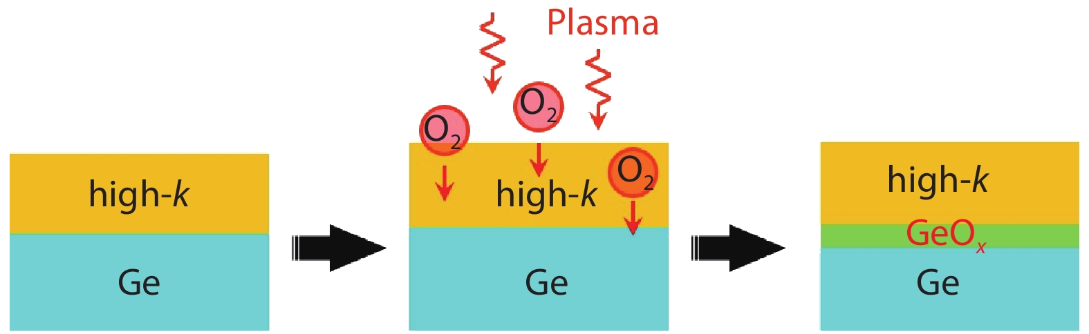
    Fig. 1. (Color online) The fabrication process of the high-k/GeOx/Ge gate stacks with PPO method.
    (Color online) The AR-XPS spectra taken from an 1-nm-thick Al2O3/Ge structure with 650 W PPO for 10 s.
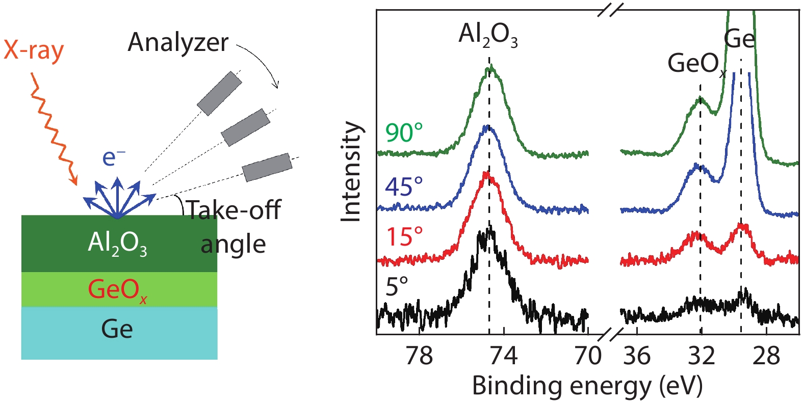
    Fig. 2. (Color online) The AR-XPS spectra taken from an 1-nm-thick Al2O3/Ge structure with 650 W PPO for 10 s.
    (Color online) (a) The C–V characteristics of an Au/Al2O3 (1 nm)/GeOx (1.2 nm)/Ge MOS capacitor fabricated with the PPO method. (b) The Dit at the Al2O3/Ge MOS interfaces w/ and w/o PPO treatment.
    Fig. 3. (Color online) (a) The C–V characteristics of an Au/Al2O3 (1 nm)/GeOx (1.2 nm)/Ge MOS capacitor fabricated with the PPO method. (b) The Dit at the Al2O3/Ge MOS interfaces w/ and w/o PPO treatment.
    (Color online) The Dit at Ei – 0.2 eV taken from PPO Al2O3/GeOx/Ge MOS interfaces fabricated with different Al2O3 capping thickness, plasma power and oxidation time.
    Fig. 4. (Color online) The Dit at Ei – 0.2 eV taken from PPO Al2O3/GeOx/Ge MOS interfaces fabricated with different Al2O3 capping thickness, plasma power and oxidation time.
    (Color online) (a) The C–V curves of the Au/HfO2/p-Ge MOS capacitors w/ and w/o PPO, compared with that of Au/Al2O3/GeOx/p-Ge MOS capacitor. (b) The C–V curves of of the Au/HfO2/Al2O3/p-Ge MOS capacitor after PPO. The inset of it shows the energy distribution of Dit of this MOS capacitor.
    Fig. 5. (Color online) (a) The C–V curves of the Au/HfO2/p-Ge MOS capacitors w/ and w/o PPO, compared with that of Au/Al2O3/GeOx/p-Ge MOS capacitor. (b) The C–V curves of of the Au/HfO2/Al2O3/p-Ge MOS capacitor after PPO. The inset of it shows the energy distribution of Dit of this MOS capacitor.
    The cross section TEM image of an HfO2 (2.2 nm)/Al2O3 (0.2 nm)/Ge structure after 15 s’ PPO using 500 W plasma.
    Fig. 6. The cross section TEM image of an HfO2 (2.2 nm)/Al2O3 (0.2 nm)/Ge structure after 15 s’ PPO using 500 W plasma.
    (Color online) The Dit at the energy of Ei – 0.2 eV of the HfO2/Al2O3/GeOx/Ge and Al2O3/GeOx/Ge gate stacks, as a function of EOT.
    Fig. 7. (Color online) The Dit at the energy of Ei – 0.2 eV of the HfO2/Al2O3/GeOx/Ge and Al2O3/GeOx/Ge gate stacks, as a function of EOT.
    (Color online) The schematic illusion of the ozone post oxidation process.
    Fig. 8. (Color online) The schematic illusion of the ozone post oxidation process.
    Cross section TEM of an HfO2 (2 nm)/Al2O3 (0.3 nm)/Ge structure after OPO for 60 s at 300 °C.
    Fig. 9. Cross section TEM of an HfO2 (2 nm)/Al2O3 (0.3 nm)/Ge structure after OPO for 60 s at 300 °C.
    (Color online) The EOT of the OPO HfO2/Al2O3/GeOx/Ge gate stacks with different Al2O3 thicknesses and OPO times.
    Fig. 10. (Color online) The EOT of the OPO HfO2/Al2O3/GeOx/Ge gate stacks with different Al2O3 thicknesses and OPO times.
    (Color online) The Dit at the energy of Ei – 0.2 eV in OPO HfO2/Al2O3/GeOx gate stacks, compared with the PPO gate stacks as a function of EOT.
    Fig. 11. (Color online) The Dit at the energy of Ei – 0.2 eV in OPO HfO2/Al2O3/GeOx gate stacks, compared with the PPO gate stacks as a function of EOT.
    (Color online) The oxide thickness of the PPO and OPO gate stacks at side wall and top regions of a 3D structured Ge channel.
    Fig. 12. (Color online) The oxide thickness of the PPO and OPO gate stacks at side wall and top regions of a 3D structured Ge channel.
    (Color online) The fabrication process of the Ge MOSFETs with OPO HfO2/Al2O3/GeOx gate stacks.
    Fig. 13. (Color online) The fabrication process of the Ge MOSFETs with OPO HfO2/Al2O3/GeOx gate stacks.
    (Color online) The Id–Vd (a) and Id–Vg (b) characteristics of an (100)/ HfO2/Al2O3/GeOx/Ge pMOSFET fabricated by 60 s OPO.
    Fig. 14. (Color online) The IdVd (a) and IdVg (b) characteristics of an (100)/<110> HfO2/Al2O3/GeOx/Ge pMOSFET fabricated by 60 s OPO.
    (Color online) The hole mobility in HfO2/Al2O3/GeOx/Ge pMOSFET fabricated by OPO with different oxidation times, compared with that in the HfO2/Al2O3/Ge pMOSFET.
    Fig. 15. (Color online) The hole mobility in HfO2/Al2O3/GeOx/Ge pMOSFET fabricated by OPO with different oxidation times, compared with that in the HfO2/Al2O3/Ge pMOSFET.
    (Color online) The mechanism of suppressed carrier scattering in the Si passivated GeSn channel, compared with the direct oxide/GeSn channel.
    Fig. 16. (Color online) The mechanism of suppressed carrier scattering in the Si passivated GeSn channel, compared with the direct oxide/GeSn channel.
    The cross section TEM image of a GeSn MOS structure having the Si passivation.
    Fig. 17. The cross section TEM image of a GeSn MOS structure having the Si passivation.
    (Color online) (a) Id–Vg and (b) Id–Vd characteristics of the (100) GeSn QW pMOSFET with Si passivation.
    Fig. 18. (Color online) (a) IdVg and (b) IdVd characteristics of the (100) GeSn QW pMOSFET with Si passivation.
    (Color online) The hole mobility in the Si passivated GeSn QW pMOSFETs with different channel orientations of (100), (110) and (111).
    Fig. 19. (Color online) The hole mobility in the Si passivated GeSn QW pMOSFETs with different channel orientations of (100), (110) and (111).
    (Color online) The comparison of (a) Id–Vd curves, (b) Gm curves and (c) hole mobility of GeSn QW pMOSFETs with different Sn contents of 2.7%, 4.0% and 7.5%.
    Fig. 20. (Color online) The comparison of (a) IdVd curves, (b) Gm curves and (c) hole mobility of GeSn QW pMOSFETs with different Sn contents of 2.7%, 4.0% and 7.5%.
    (Color online) The equienergy contours of heavy hole sub-band for GeSn pMOSFETs with different Sn contents of 2.7%, 4.0% and 7.5%, at a Ns of 5 × 1012 cm–2. The equienergy contour lines are for multiples of 20 meV.
    Fig. 21. (Color online) The equienergy contours of heavy hole sub-band for GeSn pMOSFETs with different Sn contents of 2.7%, 4.0% and 7.5%, at a Ns of 5 × 1012 cm–2. The equienergy contour lines are for multiples of 20 meV.
    Ran Cheng, Zhuo Chen, Sicong Yuan, Mitsuru Takenaka, Shinichi Takagi, Genquan Han, Rui Zhang. Mobility enhancement techniques for Ge and GeSn MOSFETs[J]. Journal of Semiconductors, 2021, 42(2): 023101
    Download Citation