
Ran Cheng, Zhuo Chen, Sicong Yuan, Mitsuru Takenaka, Shinichi Takagi, Genquan Han, Rui Zhang. Mobility enhancement techniques for Ge and GeSn MOSFETs[J]. Journal of Semiconductors, 2021, 42(2): 023101
- Journal of Semiconductors
- Vol. 42, Issue 2, 023101 (2021)
Abstract
1. Introduction
In the past few decades, the device scaling of Si metal–oxide–semiconductor field-effect transistors (MOSFETs), following Moore’s Law, drives the fast development of complementary metal–oxide–semiconductor (CMOS) integrated circuits[
It is essential to employ the high-k dielectrics (such as Al2O3, HfO2, etc.) for thinner equivalent oxide thickness (EOT), to satisfy the requirement of device scaling. Although the thin EOT high-k/Ge and high-k/GeSn MOSFETs have been demonstrated, the relatively low inversion carrier mobility severely limits the application of Ge and GeSn channels. This phenomenon attributes to the large interface state density (Dit) at the Ge and GeSn metal–oxide–semiconductor (MOS) interfaces, especially for the ultrathin Ge and GeSn gate stacks[
In this paper, the MOS interface passivation techniques from our previous work will be summarized for Ge and GeSn MOSFETs. Ge and GeSn MOSFETs with ultrathin EOT and superior channel mobility have been demonstrated, suggesting the great potential of Ge and GeSn MOSFETs as the alternative device structures in future advanced CMOS technologies.
2. Ge MOSFETs
2.1. EOT scaling and MOS interface passivation
Because of the large Dit at direct high-k/Ge interface, an interfacial layer (IL) is necessary to obtain the high mobility in Ge MOSFETs. It has been confirmed that the thermally oxidized GeO2/Ge interfaces are effective to passivate the Ge MOS interface, with a GeO2 thickness of ~20 nm[
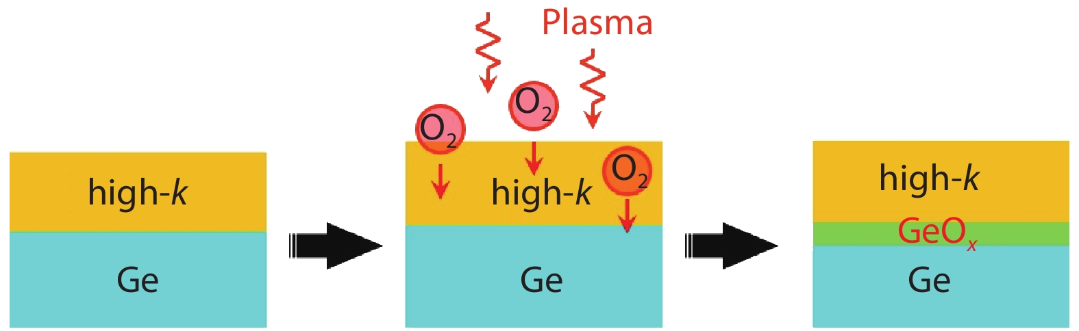
To fabricate ultrathin Ge MOS interfaces with low Dit, a plasma post oxidation (PPO) method was proposed by using oxygen plasma exposure to oxidize the high-k/Ge interface (Fig. 1), yielding a high-k/GeOx/Ge gate stack[
![]()
Figure 1.(Color online) The fabrication process of the high-
![]()
Figure 2.(Color online) The AR-XPS spectra taken from an 1-nm-thick Al2O3/Ge structure with 650 W PPO for 10 s.
The electrical properties of the PPO GeOx/Ge MOS interfaces were investigated using the Au/Al2O3/GeOx/Ge MOS capacitors. Fig. 3(a) shows the C–V curves of an Au/Al2O3 (1 nm)/GeOx (1.2 nm)/Ge MOS capacitor fabricated by PPO. The superior C–V characteristics are observed with an EOT of 1.06 nm. The Dit of this MOS capacitor was evaluated by the low temperature conductance method with the correction of surface potential fluctuation[
![]()
Figure 3.(Color online) (a) The
![]()
Figure 4.(Color online) The
The GeOx IL shows a superior scalability to maintain the low Dit for Ge MOS interfaces, indicating a possibility to realize high quality Ge gate stacks with ultrathin EOT. The suppression of EOT contributed by a high-k layer is also important. The formation of high quality GeOx/Ge MOS interfaces has been studied for HfO2/Ge structures. The strong inter-mixing between HfO2 and Ge at high temperature induces the generation of MOS interface defects[
![]()
Figure 5.(Color online) (a) The
![]()
Figure 6.The cross section TEM image of an HfO2 (2.2 nm)/Al2O3 (0.2 nm)/Ge structure after 15 s’ PPO using 500 W plasma.
The impact of the PPO time on Dit and EOT of the Au/HfO2 (2.2 nm)/Al2O3 (0.2 nm)/GeOx/p-Ge MOS capacitors were examined. The Dit values at Ei ‒ 0.2 eV of these MOS capacitors are summarized in Fig. 7 as a function of EOT. The Dit taken from the PPO Al2O3/GeOx/Ge gate stacks is also shown for comparison. Due to the drastic increase of the gate leakage of the Al2O3/GeOx/Ge gate stacks with decreasing Al2O3 thickness, the thickness of GeOx IL has to be reduced to further scale down the EOT of Al2O3/GeOx/Ge gate stacks. As a result, the clear degradation of the MOS interface quality is observed as EOT approaches ~1 nm for Al2O3/GeOx/Ge gate stacks because of the insufficient GeOx IL thickness[
![]()
Figure 7.(Color online) The
It is noted that in the HfO2/Al2O3/GeOx/Ge gate stacks, the thickness of the HfO2 layer was fixed at 2.2 nm to sufficiently suppress the gate leakage, while the EOT scaling capability of this gate stack structure is dominated by the GeOx IL thickness. Thus, it is still challenging to realize Ge gate stacks with thinner EOT but decently passivated MOS interface. Additionally, due to the directional nature of the oxygen plasma, it is difficult to realize an isotropic oxidation to 3D-structured Ge channels with the oxygen plasma. This phenomenon reduces the effectiveness of the PPO method to Ge FinFET or Ge gate-all-around devices, which are the most promising device structures for future Ge CMOS technology.
To solve these problems, an ozone post oxidation (OPO) was employed to form ultrathin Ge gate stacks with an isotropic oxidation (Fig. 8). After the ALD deposition of HfO2/Al2O3/Ge structures, the in-situ OPO was carried out at 300 °C in the 10% O3/O2 ambient with a pressure of ~100 Pa. The formation of the GeOx/Ge interface by OPO was examined by the cross-sectional TEM observation. As shown in Fig. 9, the gate stack with 60 s OPO shows a total physical thickness of 2.7 nm after 60 s OPO, indicating the growth of 0.4-nm-thick GeOx IL compared with the gate stack before OPO (2 nm HfO2/0.3 nm Al2O3). Here, the 0.3-nm-thick Al2O3 layer serves as a blocking layer to prevent the inter-mixing between HfO2 and GeOx during OPO. The partially crystallized HfO2 regions were observed in the HfO2 layer, which results in the increase of k value for HfO2[
![]()
Figure 8.(Color online) The schematic illusion of the ozone post oxidation process.
![]()
Figure 9.Cross section TEM of an HfO2 (2 nm)/Al2O3 (0.3 nm)/Ge structure after OPO for 60 s at 300 °C.
![]()
Figure 10.(Color online) The EOT of the OPO HfO2/Al2O3/GeO
![]()
Figure 11.(Color online) The
The effectiveness of the OPO method to the 3D-structured Ge channels was also examined using a series of Ge fins with the same fin height and different fin widths. The EOT on the sidewall and the EOT on the fin top are extracted for the PPO Al2O3/GeOx/Ge and the OPO HfO2/Al2O3/GeOx/Ge gate stacks. As shown in Fig. 12, the PPO Al2O3/GeOx/Ge gate stack has a thinner oxide thickness on the sidewall region than that at the bottom region, due to the insufficient formation of GeOx IL at the sidewall. In contrast, the OPO HfO2/Al2O3/GeOx/Ge gate stack shows almost the same oxide thickness for sidewall and bottom regions, meaning that the OPO exhibits an isotropic formation of GeOx IL. These results indicate the feasibility of OPO passivation for 3D-structured Ge channels.
![]()
Figure 12.(Color online) The oxide thickness of the PPO and OPO gate stacks at side wall and top regions of a 3D structured Ge channel.
2.2. Ultrathin EOT and high mobility Ge MOSFETs
The Ge MOSFETs have been demonstrated with the ultrathin EOT HfO2/Al2O3/GeOx gate stacks with OPO treatment. Gate first process was employed to fabricate the Ge MOSFETs with a structure shown in Fig. 13. The (100) n-Ge substrates with a resistivity of 1–10 Ω·cm were used. The SiO2 field oxide was deposited and the active areas were defined by etching off the SiO2. The HfO2/Al2O3/GeOx gate stacks were fabricated, and TiN gate electrodes were sputtered for the compatibility of process integration. The NiGe metal S/D structures were formed by Ni deposition and
![]()
Figure 13.(Color online) The fabrication process of the Ge MOSFETs with OPO HfO2/Al2O3/GeO
NiGe metallization at 400 °C for 1 min. Finally, Ni contact pads were deposited on gate and S/D regions by thermal evaporation, for electrical characterization.
Figs. 14(a) and 14(b) show the Id–Vd and Id–Vg characteristics of an HfO2/Al2O3/GeOx/Ge pMOSFETs with 60 s OPO, respectively. The ON/OFF ratios of the NiGe S/D pMOSFETs are ~3.5 orders of magnitude. The S factor of 85 mV/decade could be obtained for the device, which corresponds to a Dit of 2.3 × 1012 cm–2 eV–1 and agrees well with the Dit measured by the conductance method. The normal operations of the Ge pMOSFETs with different OPO times are also observed (data not shown). The effective hole mobility of the Ge pMOSFETs were evaluated by the split C–V method. Fig. 15 shows the hole mobility in HfO2/Al2O3/GeOx/Ge pMOSFETs with different OPO times. The Ge pMOSFETs with OPO HfO2/Al2O3/GeOx/Ge gate stacks exhibit a much better improved hole mobility than that in HfO2/Al2O3/Ge pMOSFETs, attributing to the MOS interface passivation by OPO treatment. The peak hole mobility of 130, 332, 417 cm2/(V·s) were achieved with ultrathin EOT of 0.78, 0.72, and 0.58 nm, respectively. Conventionally, the mobility decreases with the scaling down of EOT for Ge MOSFETs, due to the degradation of MOS interfaces in the thinner gate stacks. However, it is interestingly noted that the hole mobility in the OPO HfO2/Al2O3/GeOx/Ge pMOSFETs increases with the decrease of EOT. This phenomenon is attributable to the different mechanisms of EOT scaling by OPO treatment and the conventional interface engineering techniques for Ge gate stacks. The EOT scaling was achieved by the permittivity enhancement of HfO2 after OPO treatment for the HfO2/Al2O3/GeOx/Ge gate stacks, rather than the decrease of GeOx interfacial layer thickness obtained from the conventional Ge gate stack treatments. Thus, the EOT scaling and mobility improvement are both realized for the OPO HfO2/Al2O3/GeOx/Ge MOSFETs.
![]()
Figure 14.(Color online) The
![]()
Figure 15.(Color online) The hole mobility in HfO2/Al2O3/GeO
3. GeSn MOSFETs
3.1. MOS interface passivation
From the viewpoint of pursuing high mobility transistors, the alternative semiconductor materials are desired to further improve the CMOS performance. Although the Ge MOSFETs show promising properties to achieve an enhanced performance than the Si MOSFETs, the alternative channel materials are still mandatory for higher mobility MOSFETs. The GeSn channel MOSFETs are investigated as one of the possible solutions for future high mobility MOSFETs, especially for the high mobility pMOSFET applications. In contrast to the superior interface qualities of oxidation SiO2/Si and GeO2/Ge MOS interfaces, the oxidation GeSnOx/GeSn interface exhibits relatively high defect density[
![]()
Figure 16.(Color online) The mechanism of suppressed carrier scattering in the Si passivated GeSn channel, compared with the direct oxide/GeSn channel.
The Si passivation layers are grown on the surface of 6-nm-thick (100), (110) and (111) Ge0.92Sn0.08/Ge structures using MBE, with Si2H6 as the precursor. Fig. 17 shows the cross-section TEM image of a GeSn pMOSFET fabricated with the Si passivated GeSn substrate. Uniform layer thickness and sharp interface are observed for the Si/GeSn structure, indicating the successful formation of the GeSn quantum well channel. The pMOSFET devices with Si passivated Ge0.92Sn0.08 quantum well channels were fabricated with a gate first process. The TaN/HfO2 gate stacks were deposited on the Si/GeSn/Ge structures, followed by a post deposition annealing at 450 °C. After the gate patterning, the boron implantation and activation annealing were carried out to form the source/drain regions. The fabricated GeSn pMOSFETs exhibit normal operations as indicated by the Id–Vg and Id–Vd characteristics (Fig. 18). The peak mobility of 685, 745, and 845 cm2/(V·s) are obtained for (100), (110), and (111) GeSn pMOSFETs, respectively (Fig. 19). Additionally, the (100), (110), and (111) GeSn pMOSFETs exhibit the mobility of 445, 571, and 576 cm2/(V·s) at an Ns of 1013 cm–2, which is improved by 1.5 times as compared with those in the Ge pMOSFET control sample. The much higher hole mobility in the GeSn pMOSFETs as compared with that in Ge pMOSFETs are attributable to the high bulk mobility in GeSn and the carrier confinement effect by the Si passivation layer.
![]()
Figure 17.The cross section TEM image of a GeSn MOS structure having the Si passivation.
![]()
Figure 18.(Color online) (a)
![]()
Figure 19.(Color online) The hole mobility in the Si passivated GeSn QW pMOSFETs with different channel orientations of (100), (110) and (111).
3.2. Channel strain engineering
Beside of the MOS interface passivation, the strain engineering is also an effective performance booster to improve the mobility for GeSn pMOSFETs. It is found that the compressive strain induces the reduction of the hole effective mass and valence band edge lifting for GeSn channels, resulting in a higher hole mobility, which is similar to those in strained SiGe and Ge channels[
Fig. 20(a) shows the Id–Vd characteristics of the GeSn pMOSFETs with different Sn contents of 2.7%, 4.0% and 7.5%. The Id increase has been obtained for the GeSn pMOSFETs with the increased Sn content, which is attributable to the mobility enhancement. A similar phenomenon is also observed in the transconductance curves of these devices (Fig. 20(b)). It is also noted that the OFF-state current is larger for the GeSn pMOSFET with a higher Sn content, possibly caused by the reduced band gap due to the valent band edge lifting. The hole mobility in the GeSn pMOSFETs with different Sn contents are shown in Fig. 20(c). The improved hole mobility is confirmed for the GeSn pMOSFETs with an increase of Sn content, as theoretically predicted. The peak mobility of 340, 378, and 496 cm2/(V·s) are achieved for the GeSn pMOSFETs with Sn contents of 2.7%, 4.0%, and 7.5%, respectively.
![]()
Figure 20.(Color online) The comparison of (a)
The physical origin of the enhanced hole mobility in the GeSn channel with increased Sn content is investigated by performing the subband calculation using the 8 × 8 k∙p method, Schrödinger equation, and Poisson equation, with the material parameters taken from the Refs. [46, 47]. Fig. 21 shows the equi-energy contour plots of heavy hole (HH) bands for GeSn with different Sn contents of 2.7%, 4.0%, and 7.5%. It is found that the effective mass of hole decreases with the increase of Sn content, which is responsible for the increase of hole mobility in GeSn pMOSFETs.
![]()
Figure 21.(Color online) The equienergy contours of heavy hole sub-band for GeSn pMOSFETs with different Sn contents of 2.7%, 4.0% and 7.5%, at a
4. Conclusion
The Ge and GeSn channel MOSFETs have been examined to further improve the performance of CMOS technology. It is found that through the interface passivation with ultrathin GeOx layer grown by plasma post oxidation method, the mobility of Ge MOSFETs is sufficiently improved due to the Dit reduction. In addition, it is also confirmed that the Si passivation technique is an effective technique to enhance the mobility in the GeSn channel by suppressing the carrier scattering and reducing the hole effective mass especially for transistors with higher Sn content. These results indicate that the Ge and GeSn channels are one of the most promising solutions to realize future high-performance CMOS devices.
Acknowledgements
This work was supported, in part, by the Zhejiang Provincial Natural Science Foundation of China under Grant LR18F040001 and in part by the Fundamental Research Funds for the Central Universities.
References
[1] K Kuhn. Considerations for ultimate CMOS scaling. IEEE Trans Electron Devices, 59, 1813(2012).
[2] C Auth, A Aliyarukunju, M Asoro et al. A 10 nm high performance and low-power CMOS technology featuring 3rd generation FinFET transistors, self-aligned quad patterning, contact over active gate and cobalt local interconnects. IEDM Tech Dig, 29.1(2017).
[3] S Narasimha, B Jagannathan, A Ogino et al. A 7 nm CMOS technology platform for mobile and high performance compute application. IEDM Tech Dig, 29.5(2017).
[4]
[5] K Rim, J Welser, J L Hoyt et al. Enhanced hole mobilities in surface-channel strained-Si p-MOSFETs. IEDM Tech Dig, 517(1995).
[6] S Takagi, J L Hoyt, J J Welser et al. Comparative study of phonon-limited mobility of two-dimensional electrons in strained and unstrained Si metal–oxide–semiconductor field-effect transistors. J Appl Phys, 80, 1567(1996).
[7] S Takagi, T Mizuno, T Tezuka et al. Channel structure design, fabrication and carrier transport properties of strained-Si/SiGe-on-insulator (strained-SOI) MOSFETs. IEDM Tech Dig, 57(2003).
[8] H Shang, M M Frank, E P Gusev et al. Germanium channel MOSFETs: Opportunities and challenges. IBM J Res Dev, 50, 377(2006).
[9] K C Saraswat, C O Chui, T Krishnamohan et al. Ge based high performance nanoscale MOSFETs. Microelectron Eng, 80, 15(2005).
[10] S Gupta, R Chen, B Magyari-Kope et al. GeSn technology: Extending the Ge electronics roadmap. IEEE Tech Dig, 16.6(2011).
[11] X Gong, G Q Han, F Bai et al. Germanium-tin (GeSn) p-channel MOSFETs fabricated on (100) and (111) surface orientations with sub-400 oC Si2H6 passivation. IEEE Electron Device Lett, 34, 339(2013).
[12] R R Lieten, T Maeda, W Jevasuwan et al. Tensile-strained GeSn metal-oxide-semiconductor field-effect transistor devices on Si (111) using solid phase epitaxy. Appl Phys Exp, 6, 101301(2013).
[13] R Xie, T H Phung, W He et al. High mobility high-k/Ge pMOSFETs with 1 nm EOT – New concept on interface engineering and interface characterization. IEDM Tech Dig, 393(2008).
[14] J Mitard, C Shea, B DeJaeger et al. Impact of EOT scaling down to 0.85 nm on 70 nm Ge-pFETs technology with STI. VLSI Symp Tech Dig, 82(2009).
[15] Y Kamata, K Ikeda, Y Kamimuta et al. High-k/Ge p- & n-MISFETs with strontium germanide interlayer for EOT scalable CMIS application. VLSI Symp Tech Dig, 211(2009).
[16] S Gupta, B Vincent, B Yang et al. Towards high mobility GeSn channel nMOSFETs: Improved surface passivation using novel ozone oxidation method. IEDM Tech Dig, 16.2(2012).
[17] L Liu, R R Liang, J Wang et al. Hole mobility enhancement of GeSn/Ge pMOSFETs with an interlayer formed by Sn-assisted oxynitridation. ECS Solid State Lett, 3, Q76(2014).
[18] T Haffner, M A Mahjoub, S Labau et al. Improvement of the electrical performance of Au/Ti/HfO2/Ge0.9Sn0.1 p-MOS capacitors by using interfacial layers. Appl Phys Lett, 115, 171601(2019).
[19] Y Nakakita, R Nakane, T Sasada et al. Interface-controlled self-align source/drain Ge p-channel metal-oxide-semiconductor field-effect transistors fabricated using thermally oxidized GeO2 interfacial layers. Jpn J Appl Phys, 50, 010109(2011).
[20] K Morii, T Iwasaki, R Nakane et al. High performance GeO2/Ge nMOSFETs with source/drain junctions formed by gas phase doping. IEEE Electron Device Lett, 31, 1092(2010).
[21] C H Lee, T Nishimura, T Tabata et al. Ge MOSFETs performance: Impact of Ge interface passivation. IEDM Tech Dig, 416(2010).
[22] R Zhang, T Iwasaki, N Taoka et al. Al2O3/GeOx/Ge gate stacks with low interface trap density fabricated by electron cyclotron resonance plasma postoxidation. Appl Phys Lett, 98, 112902(2011).
[23] R Zhang, T Iwasaki, N Taoka et al. Impact of GeO
[24] R Zhang, T Iwasaki, N Taoka et al. High-mobility Ge pMOSFET with 1-nm-thick EOT Al2O3/GeO
[25] R Zhang, P C Huang, J C Lin et al. High-mobility Ge p- and n-MOSFET with 0.7-nm EOT using HfO2/Al2O3/GeO
[26] N Taoka, K Ikeda, Y Yamashita et al. Quantitative evaluation of interface trap density in Ge-MIS interfaces. Ext Abst SSDM, 396(2006).
[27] H Matsubara, H Kumagai, S Sugahara et al. Evaluation of SiO2/GeO2/Ge MIS interface properties by low temperature conductance method. Ext Abst SSDM, 18(2007).
[28] K Martens, B D Jaeger, R Bonzom et al. New interface state density extraction method applicable to peaked and high-density distributions for Ge MOSFET development. IEEE Electron Device Lett, 27, 405(2006).
[29] J R Brews. Rapid interface parameterization using a single MOS conductance curve. Solid-State Electron, 26, 711(1983).
[30] G S Smith, P B Isaacs. The crystal structure of quartz-like GeO2. Acta Cryst, 17, 842(1964).
[31] S Van Elshocht, M Caymax, T Conard et al. Effect of hafnium germinate formation on the interface of HfO2/germanium metal oxide semiconductor devices. Appl Phys Lett, 88, 141904(2006).
[32] M Houssa, G Pourtois, M Caymax et al. First-principles study of the structural and electronic properties of (100) Ge/Ge(M)O2 interfaces (M = Al, La, or Hf). Appl Phys Lett, 92, 242101(2008).
[33] S Migita, Y Watanabe, H Ota et al. Design and demonstration of very high-k (k similar to 50) HfO2 for ultra-scaled Si CMOS. VLSI Symp Tech Dig, 119(2008).
[34] P Tsipas, S N Volkos, A Sotiropoulos et al. Germanium-induced stabilization of a very high-k zirconia phase in ZrO2/GeO2 gate stacks. Appl Phys Lett, 93, 082904(2008).
[35] D Tsoutsou, G Apostolopoulos, S Galata et al. Stabilization of a very high-k tetragonal ZrO2 phase by direct doping with germanium. Microelectron Eng, 86, 1626(2009).
[36] Y Oshima, M Shandalov, Y Sun et al. Hafnium oxide/germanium oxynitride gate stacks on germanium: Capacitance scaling and interface state density. Appl Phys Lett, 94, 183102(2009).
[37] C H Fu, K S Chang-Liao, L J Liu et al. An ultralow EOT Ge MOS device with tetragonal HfO2 and high quality Hf
[38] G Han, S Su, C Zhan, Q Zhou et al. High-mobility germanium-tin (GeSn) p-channel MOSFETs featuring metallic source/drain and sub-370 oC process modules. IEDM Tech Dig, 402(2011).
[39] S Gupta, Y C Huang, Y Kim et al. Hole enhancement in compressively strained Ge0.93Sn0.07 pMOSFETs. IEEE Electron Device Lett, 34, 58(2013).
[40] M Liu, G Han, Y Liu et al. Undoped Ge0.92Sn0.08 quantum well pMOSFETs on (001), (011) and (111) substrates with in situ Si2H6 passivation: High hole mobility and dependence of performance on orientation. VLSI Symp Tech Dig, 100(2014).
[41] T Mizuno, S Takagi, N Sugiyama et al. Electron and hole mobility enhancement in strained-Si MOSFET's on SiGe-on-insulator substrates fabricated by SIMOX technology. IEEE Electron Device Lett, 21, 230(2000).
[42] S E Thompson, M Armstrong, C Auth et al. A 90-nm logic technology featuring strained-silicon. IEEE Trans Electron Device, 51, 1790(2004).
[43] M L Lee, E A Fitzgerald, M T Bulsara et al. Strained Si, and Ge channels for high-mobility metal –oxide –semiconductor field-effect transistors. J Appl Phys, 97, 011101(2005).
[44] S Nakaharai, T Tezuka, N Sugiyama et al. Characterization of 7-nm-thick strained Ge-on-insulator layer fabricated by Ge-condensation technique. Appl Phys Phys, 83, 3516(2003).
[45] T Krishnamohan, Z Krivokapic, K Uchida et al. High-mobility ultrathin strained Ge MOSFETs on bulk and SOI with low band-to-band tunneling leakage: Experiments. IEEE Trans Electron Devices, 53, 990(2006).
[46] S Gupta, B Magyari-Kope, Y Nishi et al. Achieving direct band gap in germanium through integration of Sn alloying and external strain. J Appl Phys, 113, 073707(2014).
[47] Y Yang, K L Low, W Wang et al. Germanium-tin n-channel tunneling field-effect transistor: Device physics and simulation study. J Appl Phys, 113, 194507(2013).

Set citation alerts for the article
Please enter your email address
© Copyright 2018-2021 | Chinese Laser Press. All Rights Reserved 沪ICP备15018463号-20