
Giorgos Boras, Xuezhe Yu, Huiyun Liu. III–V ternary nanowires on Si substrates: growth, characterization and device applications[J]. Journal of Semiconductors, 2019, 40(10): 101301
- Journal of Semiconductors
- Vol. 40, Issue 10, 101301 (2019)
![(a)–(c) Scanning electron microscopy (SEM) images of InAsSb/GaSb core/shell NWs grown via MOCVD following SAG mode. The arrays of the grown NWs have a high level of homogeneity. NWs were grown with different Sb compositions, as indicated in each image. (Reprinted with permission from Ref. [34]. Copyright (2016) American Chemical Society.)](/richHtml/jos/2019/40/10/101301/img_1.jpg)
Fig. 1. (a)–(c) Scanning electron microscopy (SEM) images of InAsSb/GaSb core/shell NWs grown via MOCVD following SAG mode. The arrays of the grown NWs have a high level of homogeneity. NWs were grown with different Sb compositions, as indicated in each image. (Reprinted with permission from Ref. [34 ]. Copyright (2016) American Chemical Society.)
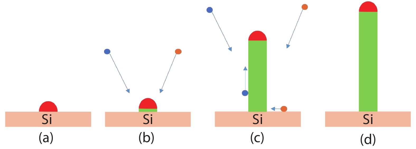
Fig. 2. (Color online) (a) Droplet is deposited on the Si substrate. (b) Elements are supplied in the reactor. The adatoms are alloyed with the liquid droplet and, after supersaturation, a monolayer is formed covering the liquid/solid interface. (c) The continuous supply of elements leads to the elongation of the NW. The adatoms reach the droplet either via direct impingement or after diffusion on the substrate and the NW sidewalls. (d) After the supply of elements is terminated, the axial growth stops.
Fig. 3. (Color online) (a) Top view and (b) front view schematic representations respectively for a GaAs NW cladded with a 20 nm thick AlInAs shell. The strain that is induced by the lattice mismatch between the core and the shell causes a severe bending of the NW. The convex side is more appropriate for adatom accommodation, further increasing this phenomenon. (Reprinted with permission from Ref. [59 ]. Copyright (2018) American Chemical Society.)
Fig. 4. (Color online) (a) SEM image of GaAsP NWs grown under V/III ratio of 50. Uniformity and vertically aligned NWs are observed. (b) SEM image of GaAsP NWs grown under V/III ratio of 75. The growth rate is reduced due to shrinkage of the droplet, causing a severe tapering in the NWs. (c) SEM image of GaAsP NWs grown under V/III ratio of 100. Large group V flux rapidly consumes the droplets and no VLS growth takes place. (d) Transmission Electron Microscopy (TEM) image of the overall and section views of a NW grown under V/III ratio of 50. In the middle of the structure, no defects are observed and the crystal adopts a pure ZB phase. The only defects are located at the top and bottom parts of the NW. The SAED pattern, a higher magnification on the droplet and a higher magnification of the part indicated by the white arrows are given in the insets. (e) A TEM image of a NW grown under V/III ratio of 75. Multiple defects are viewed in the image due to the increased flux of group V elements. The defects appear as regions of different brightness and three typical examples are shown with black arrows. (Figs. 4(a) –4(e) : Reprinted with permission from Ref. [69 ]. Copyright (2013) American Chemical Society.) (f) UV visible diffuse reflectance spectrum (absorption) of both narrow NWs (dashed line) and wide NWs (solid line) at different P contents. (g) Dependence of the bandgap on the nominal composition of P, for narrow and wide NWs. (Figs. 4(f) –4(g) : Reprinted with permission from Ref. [68 ]. Copyright (2014) American Chemical Society.) (h) SEM of NWs grown on patterned substrate, where the diameter of the holes is 50 nm and is smaller than the diameter of the droplet. A highly homogeneous NW arrays is formed. In the inset, a higher magnification of a single NW is depicted, confirming the homogeneous shape of the structure. (i) SEM image of NWs grown on patterned substrate where the diameter of the holes is 135 nm. The promotion of lateral VS growth leads to the structures taking the form of short nanopillars, as viewed in the inset. (Figs. 4(h) –4(i) : Reprinted with permission from Ref. [70 ]. Copyright (2014) American Chemical Society. Further permissions related to the material excerpted should be directed to the ACS.)
Fig. 5. (Color online) (a) TEM image of a GaAs QD embedded in a GaAsP NW. The brighter region, revealing the presence of the dot, is marked by the red circle. (b) EDX mapping of the structure. The QD section exhibits a higher As and lower P content than the NW part of NWQDs. (c) Micro PL spectra at different excitation powers from a single GaAsP/GaAs NWQD. Sharp peaks attributed to QD emission are observed at 1.66 eV. The linewidth is measured as narrow as 130 μ eV. (Figs. 5(a) –5(c) : Reprinted with permission from Ref. [71 ]. Copyright (2015) American Chemical Society.)
Fig. 6. (Color online) (a) SEM image of InAsP NWs tilted by 45°. The NWs are perpendicular to the Si substrate and their density is estimated at 5.5 × 108 cm–2. (b) Diameter distribution respectively for the InAsP NWs. High uniformity is confirmed. (c) High resolution TEM (HRTEM) of the middle part of an InAsP NW. Multiple stacking faults are observed. The inset presents the SAED pattern of this part. The streaky features confirm the formation of stacking faults. (d) HRTEM of the NW/Si interface. Misfit dislocations appear and are marked by yellow arrows in the image. In the inset the SAED pattern of the interface is shown. The clear spots reveal a pure ZB structure at the NW/Si interface, which leads to the conclusion of stacking faults being developed after the nucleation of the InAsP NWs at the initial stages of the growth. (Figs. 6(a) –6(d) : Reprinted with permission from Ref. [21 ]. Copyright (2013) American Chemical Society.) (e) Micro-PL spectrum of a single InP NW with two InAsP QD insertions. The peaks corresponding to the QDs are located at 1.401 and 1.412 μ m and are very sharp and narrow with a full width at half maximum of 120 μ eV. The narrow peaks are indicative of the 3D quantum confinement induced by the QD insertions. (Fig. 6(e) : Reprinted with permission from Ref. [76 ]. Copyright (2007) American Chemical Society.)
Fig. 7. (Color online) (a)–(c) SEM images of NWs grown on patterned substrate with pitch lengths of 1200, 800 and 400 nm, respectively. The density of the NWs is significantly increased with decreasing length of the pitch. d) PL spectra of NWs grown at different pitch lengths. Increasing size of the pitch leads to a redshift of the emission attributed to an increased presence of Sb in the NWs. That is in accordance with the Sb-richness induced by the increasing wetting angle of the droplet with enlarged holes. (Figs. 7(a) –7(d) : Reprinted with permission from Ref. [83 ]. Copyright (2016) American Chemical Society.) (e)–(f) SEM images of GaAsSb NW arrays grown under Sb flux of 2 × 10⁻⁷ and 8 × 10⁻⁷ Torr, respectively. Increasing Sb flux, thus enhanced Sb content, leads to a significant increase in the diameter of the NWs. (g) Graph of the diameter and the length of the NWs as a function of the Sb flux. Increasing Sb flux causes an increase in the diameter of the NWs as a result of the surfactant effect and a reduction in the length of the structures as a result of the poisoning effect. (h) BF-TEM image of a GaAs NW with a GaAsSb segment embedded inside. The red square and the orange square mark the bottom and top part of the segment, respectively. (i) High Resolution TEM image of the red square of Fig. 7(h) . The incorporation of Sb in the NW leads to a rapid WZ to ZB transition. (j) High Resolution TEM image of the orange square of Fig. 7(h) . Beyond the length of the GaAsSb segment, the crystal phase transits back into WZ. (Figs. 7(e) –7(j) : Reprinted with permission from Ref. [29 ]. Copyright (2016) American Chemical Society.)
Fig. 8. (Color online) (a) Normalized PL spectra of GaAsSb NWs grown on Si substrates, with different Sb content. The measurements are taken at 77 K and the wavelength of the emission reaches 1480 nm. (b) Normalized PL spectra of GaAsSb NWs grown on GaAs stems, with different Sb content. The measurements are taken at 77 K and the wavelength of the emission reaches 1760 nm. (Reprinted with permission from Ref. [52 ]. Copyright (2017) American Chemical Society.)
Fig. 9. (Color online) (a) SEM image of InAsSb NWs grown at 470 °C. The structures are vertically aligned on the (111)-oriented substrate. (b) SEM image of InAsSb NWs grown at 450 °C. The decreasing temperature forces the NWs to change orientation and elongate planar on the substrates. (Figs. 9(a) and 9(b) : Reprinted with permission from Ref. [91 ]. Copyright (2015) American Chemical Society.) (c)–(f) High resolution TEM of catalyst free InAs(Sb) NWs grown via the catalyst-free method at different Sb content as indicated in the images. White arrows show the direction of the growth. Increasing Sb content leads to a transition from WZ dominant to pure ZB crystal phase due to the surfactant effect of Sb. (Figs. 9(c) –9(f) : Reprinted with permission from Ref. [30 ]. Copyright (2014) American Chemical Society.) (g) PL spectra of InAsSb NWs with Sb content of 0, 3%, 10%, 16% and 19%, respectively. The shrinkage of the bandgap leads to peaks covering the entire mid-infrared region, reaching 0.23 eV. No QW-like peaks are noticed, due to the single crystallinity of the NWs. (Fig. 9(g) : Reprinted with permission from Ref. [93 ]. Copyright (2017) IOP Publishing Ltd.)
Fig. 10. (Color online) (a) SEM of an AlGaAs NW array grown on Si at 510 °C with a nominal composition of Al at 30%. (b) Cross sectional EDX scanning of an AlGaAs NW. The peaks of Al and dips of Ga at the external facets reveal the presence of an Al-rich shell. As expected, Arsenic is homogeneously distributed in the structure. (c) TEM image of a NW, revealing its inversed tapered shape. The darker colour of the shell reveals its higher percentage of Al. (Figs. 10(a) –10(c) : Reprinted with permission from Ref. [105 ]. Copyright (2016) American Chemical Society.) (d) PL spectrum of GaAs QDs embedded in GaAs/AlGaAs core/shell NWs. Two peaks are exhibited, X and X* attributed to exciton and biexciton transition, respectively. The linewidths for X and X* are 315 and 458 μ eV. (e) Second order correlation function of X, revealing antibunching behaviour and demonstrating the potential of the structure to act as a non-classical light source. (Figs. 10(d) –10(e) : Reprinted with permission from Ref. [107 ]. Copyright (2015) American Chemical Society.)
Fig. 11. (Color online) (a)–(h) SEM images of InGaAs NWs grown via MBE following SAG mode. The arrays of the grown NWs have a high level of homogeneity. NWs were grown at different temperatures with different Ga compositions, as indicated in each image. (i) Normalized micro PL spectra of InGaAs NWs grown at different Ga composition. A wide range of tuning is accomplished. (Figs. 11(a) –11(i) : Reprinted from Ref. [115 ] with the permission of AIP publishing.) (j) Optical image of a Si (111) wafer with InGaAs NWs grown. The slight variations in the NW density are demonstrated by the colour variations in the image. (k) and (l) SEM images for InGaAs NWs with 15% and 70% In content grown at 570 and 590 °C, respectively. Increased composition of In causes an increase in the diameter of the NWs, due to its incorporation at the external facets. (m) Micro-PL spectrum of an InGaAs NW array, with 20% In depicted as a black line. The red line corresponds to a similar array with the addition of a GaAs shell. The passivation of surface states by the shell leads to a considerable increase of the PL intensity. (Figs. 11(j) –11(m) : Reprinted with permission from Ref. [114 ]. Copyright (2011) American Chemical Society.)
Fig. 12. (Color online) (a)–(f) SEM images of InGaP NWs grown on InP substrates. The different temperatures of the growth are noted in the images. It is observed that low growth temperatures led to shorter NWs and promoted radial overgrowth (Fig. 12(a) ), while increasing temperatures induced the formation of highly homogeneous arrays of perpendicular NWs (Figs. 12(b) –12(d) ). Further increase above 750 °C in temperature led to compositional inhomogeneity that induced strain in the structures and ultimately caused their bending and non-vertical orientation (Figs. 12(e) –12(f) ). (g) CL spectra of InGaP NWs grown with different Ga composition. A blueshift related to the increased Ga content is presented with increasing flow ratio. After a critical point, polyrcrystals were formed instead of NWs. The shortest wavelength for standing NWs in this work was 799 nm, while the highest was obtained for InP NWs at 871 nm. (Figs. 12(a) –12(g) : Reprinted by permission from Springer Nature: Nano Research, Ref. [124 ]. Copyright (2017).) (i) Graph of the In content as a function of the diethylzinc molar fraction. It is clear that increasing presence of diethylzinc leads to a rapid reduction in the In composition of the structure. (j) EDS line scanning of an InGaP NW with consequent i- and p- regions. Ga peaks at the doped regions reveal increased presence of this element and confirm that the presence of diethylzinc causes a reduction in the In content and a subsequent increase in the Ga content. (Figs. 12(h) and 12(i) : Reprinted with permission from Ref. [125 ]. Copyright (2017) American Chemical Society.)
Fig. 13. (Color online) (a) Schematics of the InGaSb NW, showing the three different segments (InAs stem, InSb stem, InGaSb segment) of the structure. (b) SEM image of the wire-on-stem structures, clearly exhibiting differences in the diameter, between the consecutive segments. The scale bar is 200 nm. (c) EDX axial scanning of the NW. The InGaSb regions correspond with the increase in the Ga line (red). This segment is revealed to be Ga-rich, with approximately 60% Ga content. The scale bar is 100 nm. (Reprinted with permission from Ref. [126 ]. Copyright (2012) American Chemical Society.)
Fig. 14. (Color online) (a) SEM image of an AlInP NW array, demonstrating a high degree of morphological homogeneity. (b)–(d) High magnification SEM images of a WZ InP NW and two WZ AlInP NWs with Al content at 15% and 25%, respectively. Increasing Al content leads to a transition of the initial, hexagonal cross section to a more complex dodecagonal form, potentially due to the alterations of V/III ratio and elemental composition. (e) PL spectra of AlInP NW ensembles. Increasing Al content induces a blue shift of the peak towards the green region of the spectrum. For 0–40% Al, emission covers the range between 875 and 555 nm (infrared to green region). (Figs. 14(a) –14(e) : Reprinted with permission from Ref. [129 ]. Copyright (2018) American Chemical Society. Further permissions related to the material excerpted should be directed to the ACS.)
Fig. 15. (Color online) (a) PL spectra at room temperature for different excitation powers. The insets show a PL spectrum of FP modes below lasing threshold under a pump power density of 1.88 kW/cm2 (left) and a lasing peak with a linewidth of 0.76 nm (right). (b) PL specra of three different samples with Sb compositions of 1%, 5% and 8% for samples A, B and C, respectively. Increasing Sb presence leads to a redshift of the lasing peak enabling tunability between 890 and 990 nm. (Figs. 15(a) and 15(b) : Reprinted with permission from Ref. [132]. Copyright (2018) American Chemical Society.) (c) Lasing from an InGaAs nanopillars surrounded by GaAs shell, at 950 nm. The device operated up to room temperature (293 K). (d) PL spectra from InGaAs/GaAs core/shell nanopillars exhibiting lasing at different wavelengths as a function of the nominal composition of In. The In content of the core was varied between 12% and 20% leading to a control of lasing between 890 and 940 nm. (Figs. 15(c) and 15(d) : Reprinted by permission from Springer Nature: Nat Photonics, Ref. [109 ]. Copyright (2011).) (e) Cross-sectional TEM image of a GaAs/(In,Al)GaAs core/shell NW with InGaAs QWs embedded in the shell. (f) PL spectra of the structure of Fig. 15(e) at 10 K, exhibiting lasing with tunability from 1.36 to 1.57 eV for In composition ranging between 0 and 40%. (g) Similar spectra at room temperature exhibiting tunability up to 30% In content. (Figs. 15(e) –15(g) : Reprinted with permission from Ref. [133 ]. Copyright (2018) American Chemical Society.) (h) PL spectra from InGaAs NW grown on SOI exhibiting tuneable emission, covering 1.33 and 1.51 μ m telecommunication windows via tuning of their In composition. (Fig. 15(h) : Reprinted with permission from Ref. [135 ]. Copyright (2016) American Chemical Society.)
Fig. 16. (Color online) (a) SEM of a GaAsP NW solar cell with InGaAs passivation layer. The scale bar is 1 μ m. (b) P–V comparison between the passivated (red) and the unpassivated (blue) GaAsP NWs. The power reaches a maximum of 10.2 mW/cm2 for the passivated NWs while remaining at 6.8 mW/cm2 for unpassivated NWs. (Figs. 16(a) and 16(b) : Reprinted with permission by Springer Nature: Nature Communications, Ref. [140 ]. Copyright (2013)) (c) Schematics of photovoltaic solar cell structures based on InGaAs/AlInAs NWs on Si. (d) I –V curve in dark for InGaAs/AlInAs NWs showing a clear rectifying, diode-like behaviour. The ideality factor is extracted as 2.5. (e) Comparison of the I–V curves in dark and under illumination for passivated and unpassivated NWs. The curve of the unpassivated NWs exhibits S-shape behaviour, indicative of losses and low efficiency, which is absent from core/shell NWs. (Figs. 16(c) –16(e) : Reprinted with permission from Ref. [20 ]. Copyright (2015) American Chemical Society. Further permissions related to this material excerpted should be directed to the ACS.) (f) I–V curve of solar cells based on InAsP NWs. Clear diode, rectifying behaviour is exhibited. The ideality factor is small at 1.4 and comparable to the up-to-date NW solar cell technologies. (Fig. 16(f) : Reprinted with permission from Ref. [21 ]. Copyright (2013) American Chemical Society.)
Fig. 17. (Color online) (a) Schematics of the GaAsP NW, showing the growth of the p-type core and n-type shell, with an intrinsic shell between the two. (b) Schematics of a water splitting device consisted of a NW array grown on Si substrates. (c) Current density potential characteristics of GaAsP homojunction NWs photocathode. (d) Current density potential characteristics of GaAsP NWs photocathode with the addition of an InGaAs passivation shell. The insets in Figs. 17(c) –17(d) show the steady-state current density of the photocathodes. The measurements were conducted at 0.1 V versus RHE under AM 1.5G illumination. (Figs. 17(a) –17(d) : Reprinted with permission from Ref. [22 ]. Copyright (2014) American Chemical Society. Further permissions related to the material excerpted should be directed to the ACS.)
Fig. 18. (Color online) (a) SEM image of a single GaAsSb NW-based device with four metal electrodes. The scale bar is 500 nm. (b) I–V curve of a single GaAsSb NW in four-probe geometry (A–D). Probe A is close to the tip and D is close to the base as viewed in the SEM image of Fig. 18(a) . Rectifying behaviour is clearly observed in all configurations (with the C–D measurement closer to the base being more pronounced). (c) I–V curves under different illuminations of the photodetector fabricated by GaAsSb NWs that gave the measurements of Fig. 18(b) . The rectifying behaviour observed is a result of the asymmetric Schottky contacts formed at the NW ends. The inset shows the photocurrent as a function of the intensity of illumination. The photoresponsivity is calculated as 1463 A/W. (Figs. 18(a) –18(c) : Reprinted with permission from Ref. [79 ]. Copyright (2015) American Chemical Society.). (d) Schematics of a photodetector based on an array of GaAsSb/AlGaAs core/shell NWs. (e) I–V curves of the photodetector of Fig. 18(d) under different illuminations. Rectifying behaviour indicates the existence of asymmetric Schottky contacts at both NW ends. (f) I–V curve of the device of Fig. 18(d) . The photocurrent has a high value at forward bias, due to previous NW annealing. The stimulated fit is depicted by the red line. (Figs. 18(d) –18(f) : Reprinted with permission from Ref. [28 ]. Copyright (2018) IOP Publishing Ltd.)
Fig. 19. (Color online) (a) SEM (top) and schematics (bottom) of a back-gated FET with metal contacts based on a single InGaAs NW. (b) Transfer characteristics of the FET of Fig. 19(a) for different V DS. The inset depicts the statistics of the I ON/I OFF ratio of 100 such devices. (Figs. 19(a) and 19(b) : Reprinted with permission from Ref. [32 ]. Copyright (2012) American Chemical Society.) (c) Transfer characteristics of three back-gated FETs based on single In0.7Ga0.3As NWs with three different diameters. Smaller NWs present reduced electron transport and mobility. (Fig. 19(c) : Reprinted Ref. [141 ] with the permission of AIP publishing.) (d) Surround-gated FET comprised of a parallel array of 10 InGaAs NWs. Each NW is composed of a Si-doped InGaAs on top of an undoped InGaAs NW. Each NW is wrapped with Hf0.8Al0.2O gate oxide and tungsten (W) gate metal. L G is 200 nm and L G-D is 50 nm. (e) Capacitance-gate voltage curve of the surround gated FET of Fig. 19(d) , with 250 parallel NWs. The inset shows the SEM of a representative structure. (f) Transfer characteristics of a surround-gated FET based on InGaAs NWs. The values of different parameters are included in the figure. (Figs. 19(d) –19(f) : Reprinted by permission from Springer Nature: Nature, Ref. [31 ]. Copyright (2012).)
Fig. 20. (Color online) (a)–(c) Tables including III–V–V, III–III–V and rare alloys, respectively, encapsulating the bandgap, growth methods, basic properties and device implementation of the ternary III–V NWs described throughout the current paper.

Set citation alerts for the article
Please enter your email address
© Copyright 2018-2021 | Chinese Laser Press. All Rights Reserved 沪ICP备15018463号-20