
Giorgos Boras, Xuezhe Yu, Huiyun Liu. III–V ternary nanowires on Si substrates: growth, characterization and device applications[J]. Journal of Semiconductors, 2019, 40(10): 101301
- Journal of Semiconductors
- Vol. 40, Issue 10, 101301 (2019)
Abstract
1. Introduction
The application of electronic and optoelectronic technologies in numerous aspects of daily life has been growing immensely over the past decades. The underlying platform on which most of the electronic and optoelectronic circuits and devices are founded is Si due to its low cost, good thermal conductivity, abundant availability and high-level maturity[
A solution that has been suggested is employing a sophisticated growth technique of buffer layer between the Si substrate and the III–V structure[
A novel method to achieve III–V growth on Si is to employ semiconductor nanowires (NWs), an emerging and promising platform that is being thoroughly investigated and rapidly developed mainly during the past two decades. The small contact area between the substrate and the NW along with the large surface to volume ratio leads to elastic strain relaxation, which allows for the monolithic growth of III–V NWs on Si substrates and thus renders the direct integration of III–V semiconductors on the Si platform feasible[
An essential aspect of NWs research that is being under substantial investigations and is employed for applications is the use of ternary NWs, where, for III–V semiconductors, two group III and one group V or two group V and one group III elements are combined. This offers a high degree of freedom in material design owing to their fully tuneable bandgap depending on the elemental composition of the alloy. Generally, the elemental composition of the alloy is determined by the growth conditions and growth methods that are used and can be tuned to great extents by altering the growth parameters. Due to this flexibility that can be approached via the optimization of the growth, ternary NWs have been implemented in multiple applications such as energy harvesting, for example, solar cells[
In this review, we will present the recent advances in the growth and characterization of ternary III–V NWs grown on Si substrates. By examining the rich literature on this vibrant field, we have summarized the III–V ternary alloys that are available in the literature in terms of the growth methods, characterization and optical properties of each ternary alloy. In the first section, we will briefly discuss the different growth mechanisms, namely the vapour-liquid-solid (VLS) growth mode, selective area growth (SAG) and catalyst-free technique and the characteristics of each of them. Then, we will describe the effect of the strain for the growth of axial heterostructures or core/shell ternary III–V NWs, which is inevitably considered due to the essential of the heterostructure growth. A thorough description of each of the ternary alloy NWs will be demonstrated in the third section, including GaAsP, AlGaAs, GaAsSb, InAsSb, InGaAs and InGaP. Particular emphasis will be given to the aspects of the growth, the crystal purity of the NWs, as well as to the optical and electrical properties of the NWs. For some of these cases, growth on substrates other than Si is briefly included for comparison or for supplementary information, which includes the description of the growth of four rare III–V alloys of InGaSb, GaPSb, InPSb and AlInP, in the third section as well. Finally, we will briefly describe the various devices that have been implemented on the ternary III–V, such as lasers, solar cells, photodetectors, water splitting and FETs and their performance and potential optimizations are discussed.
2. Growth mechanisms
Ternary III–V NWs can be grown via epitaxial techniques available such as molecular beam epitaxy (MBE), metal-organic vapour phase epitaxy (MOVPE) also known as metal-organic chemical Vapour deposition (MOCVD), chemical beam epitaxy (CBE) and chemical vapour deposition (CVD). In each of the growth systems, there are two major growth modes that are being used extensively, namely the selective-area growth (SAG) and the vapour-liquid-solid (VLS) growth mode. The progress on these fundamental growth modes for ternary NW growth is remarkable. Nevertheless, there are still several challenges met in each of them and their exact solution has not been fully unravelled yet.
SAG for ternary NWs is a growth method where the NW growth occurs through holes patterned on the substrate by the use of a mask and a lithography technique (i.e. nanoimprint lithography, electron beam lithography (EBL) etc.[
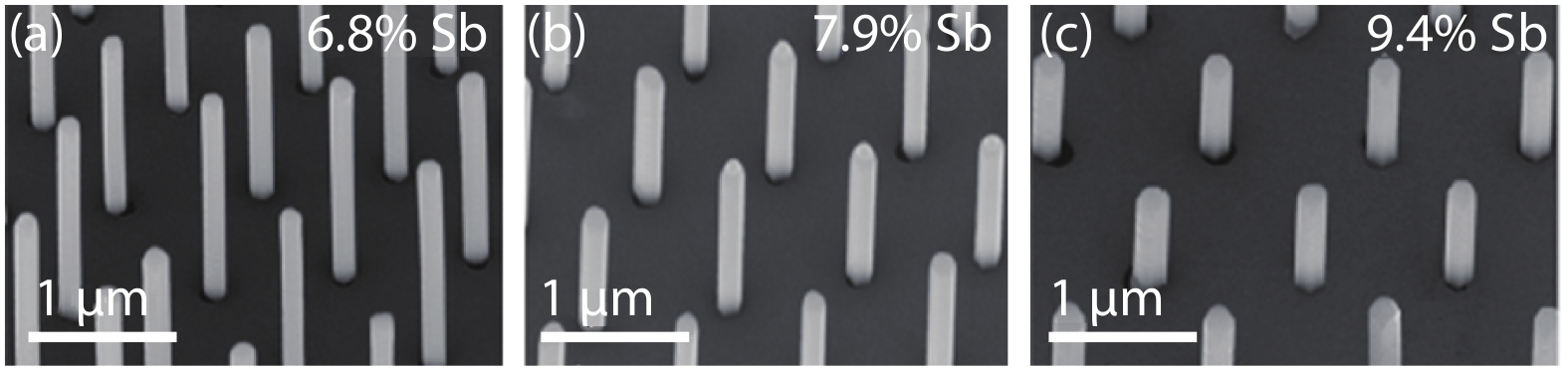
![]()
Figure 1.(a)–(c) Scanning electron microscopy (SEM) images of InAsSb/GaSb core/shell NWs grown via MOCVD following SAG mode. The arrays of the grown NWs have a high level of homogeneity. NWs were grown with different Sb compositions, as indicated in each image. (Reprinted with permission from Ref. [
VLS growth is the most popular method for the growth of ternary NWs. The growth is induced by a catalyst droplet, which can be either a foreign metal seed or an element which is also a component of the ternary NW. For ternary NWs of group III–V, group III elements can be used, for instance, Ga and In. Al can also be used as a catalyst droplet[
![]()
Figure 2.(Color online) (a) Droplet is deposited on the Si substrate. (b) Elements are supplied in the reactor. The adatoms are alloyed with the liquid droplet and, after supersaturation, a monolayer is formed covering the liquid/solid interface. (c) The continuous supply of elements leads to the elongation of the NW. The adatoms reach the droplet either via direct impingement or after diffusion on the substrate and the NW sidewalls. (d) After the supply of elements is terminated, the axial growth stops.
Due to the detrimental effects of Au on the applicability of the NWs, the need for an alternative route was emerging. This route could be the self-catalysed growth, where catalyst droplets that initiate the growth are also one of the components of the ternary NW. The growth mode is similar to the case of the foreign metal catalyst. The fact that the material of the droplet is already a component of the NW eliminates the contamination, as mentioned earlier[
As stated earlier, the reservoir effect which appears in VLS growth of ternary NWs hinders the abruptness of the interfaces[
Ternary III–V NWs have been grown via all three of the described techniques. It is highlighted, however, that due to the disadvantages of the Au droplet, self-catalysed and catalyst-free methods are particularly suitable for the growth of ternary NWs on Si substrates. In the next chapter, we will briefly describe the role of strain in NW structures, before continuing with the central part of our literature review.
3. Effect of strain
The integration of group III–V semiconductor structures with the cost-effective and mature Si platform has been hindered by the significant lattice mismatch between them, which induces high amounts of strain. The existence of strain would give rise to defects such as misfit dislocations and more importantly, threading dislocations that are formed in III–V structures. Threading dislocations are considered non-radiative recombination centres, which severely affect the intensity of the PL emission, thus degrading the performance of the resulting optoelectronic device. Other defects that may emerge include stacking faults, rotational twins, and grain boundaries. Due to the profound influence that these crystal defects have on the performance of the structures, intense efforts have been devoted to the optimization of their material quality and consequently, their optical performance.
NWs are unique compared with other nanostructures or thin films because of their large strain tolerance. Owing to their geometrical features, such as the large surface to volume ratio and the small contact area between the NW and the substrate, there is a critical radius below which the strain is elastically relaxed[
As a result of the above, it is clear that axial NWs are free of strain. It is noted that misfit dislocations can still be observed at the NW/substrate interface[
![]()
Figure 3.(Color online) (a) Top view and (b) front view schematic representations respectively for a GaAs NW cladded with a 20 nm thick AlInAs shell. The strain that is induced by the lattice mismatch between the core and the shell causes a severe bending of the NW. The convex side is more appropriate for adatom accommodation, further increasing this phenomenon. (Reprinted with permission from Ref. [
Based on the above results found in the literature, the strain can give rise to detrimental effects on the core/shell NW morphology and composition. A direct path to circumvent this obstacle is the combination of lattice-matched materials in core/shell structures. The minimum amount of strain between the core and the shell has been exploited to realize not only III–V core/shell NWs but even hybrid III–V/IV NW structures, with vast potential for optoelectronic applications[
Despite the types of strain that can be induced in the core/shell structures or intentionally applied in the NWs, the unique axial NW geometry allows for efficient, elastic strain relaxation which in turn enables compatibility of ternary III–V NWs with the mature Si platform. That property renders the NWs particularly appealing for a wide range of applications, where Si plays a crucial role such as electronics, optoelectronics and solar cells. Due to the effective elastic relaxation, strain plays a less significant role in the growth of axial NWs. The detailed investigation of core/shell architecture and the effects of strain is beyond the scope of this review. In the rest of the current report, we will focus on the growth and analysis of NWs with ternary cores.
In the following section, we will investigate the rich literature of each type of NWs that has been successfully grown, and some of them have already been applied to the prototypical devices. Particular emphasis will be given to the different aspects of the growth and to the characterization of NWs regarding their crystal structure to conclude on their material quality. A description of the optical and electrical properties of the ternary NWs will also be included. These features enable us to evaluate the suitability of these nanostructures for the fabrication of devices, which will be later analysed in the fifth section. Through this procedure the growth, characterization and device performance of ternary NWs will be discussed and clarified.
4. Ternary III–V NWs on Si
4.1. III–V–V nanowires
4.1.1. GaAsP nanowires
One of the most explored ternary NWs is GaAsP. The interest in this alloy is mainly due to the considerable frame of tunability of its bandgap, which can theoretically range between 1.43 eV (GaAs) and 2.24 eV (GaP) at room temperature. Even though GaP, as one of its edge alloys, has an indirect bandgap, GaAsP exhibits an indirect to direct transition at 44% P content[
One of the most crucial tasks during the growth of ternary NWs is defining the appropriate parameters that will determine the morphological features and the consequent properties of the structures. Among the growth parameters, the most critical one in ternary NW growth is the V/III ratio, owing to the different incorporation rates of group III and group V adatoms. By altering the V/III ratio, the morphology of the NWs can be entirely altered from uniform, standing NWs to tapered or cluster-like structures, due to changes in the geometry of the Ga droplets that initiate the growth. In the case of GaAsP NWs, at a relatively low V/III beam flux ratios of 50, the droplets are fully formed and clearly define the boundaries for the growth of the NWs (Fig. 4(a))[
![]()
Figure 4.(Color online) (a) SEM image of GaAsP NWs grown under V/III ratio of 50. Uniformity and vertically aligned NWs are observed. (b) SEM image of GaAsP NWs grown under V/III ratio of 75. The growth rate is reduced due to shrinkage of the droplet, causing a severe tapering in the NWs. (c) SEM image of GaAsP NWs grown under V/III ratio of 100. Large group V flux rapidly consumes the droplets and no VLS growth takes place. (d) Transmission Electron Microscopy (TEM) image of the overall and section views of a NW grown under V/III ratio of 50. In the middle of the structure, no defects are observed and the crystal adopts a pure ZB phase. The only defects are located at the top and bottom parts of the NW. The SAED pattern, a higher magnification on the droplet and a higher magnification of the part indicated by the white arrows are given in the insets. (e) A TEM image of a NW grown under V/III ratio of 75. Multiple defects are viewed in the image due to the increased flux of group V elements. The defects appear as regions of different brightness and three typical examples are shown with black arrows. (
The phosphoric content of GaAsP NWs is of great importance for the optical properties of the structures and is directly related to the bandgap of GaAsP. The UV visible diffuse reflectance spectrum presented in Fig. 4(f) analyses the photon absorption for NWs with a different nominal composition of P. The onset value of the absorption band is determined as the value of the bandgap of the semiconductor[
Most applications require a highly homogeneous array of NWs, which is particularly challenging, especially in the case of ternary NWs. A potential solution is the patterning of the Si substrates via lithography techniques. This method is costlier due to the additional processing steps but it is also instrumental in defining the exact position and dimensions of the NWs that form the array. The size of the holes is a vital parameter to be considered. When the size of the hole is equal or smaller than the diameter of the droplet, the latter covers the hole in its entirety, causing all of the Ga adatoms to reach the droplet and participate in the axial growth of the GaAsP NWs (Fig. 4(h)). On the contrary, when the size of the holes is larger than the diameter of the droplet, a vacant, oxide-free Si area is exposed and the Ga, P and As adatoms would cover this area and giving rise to lateral vapour-solid (VS) growth. That phenomenon reduces the number of Ga adatoms migrating to the droplet, leading to the formation of NWs with very narrow tips and mostly wide bases[
Interesting morphological and optical features can be observed after embedding a single GaAs QD axially in the GaAsP NWs[
![]()
Figure 5.(Color online) (a) TEM image of a GaAs QD embedded in a GaAsP NW. The brighter region, revealing the presence of the dot, is marked by the red circle. (b) EDX mapping of the structure. The QD section exhibits a higher As and lower P content than the NW part of NWQDs. (c) Micro PL spectra at different excitation powers from a single GaAsP/GaAs NWQD. Sharp peaks attributed to QD emission are observed at 1.66 eV. The linewidth is measured as narrow as 130
4.1.2. InAsP nanowires
InAsP is a ternary alloy with an extensive range of tunability of its bandgap. The bandgap energy varies between 0.36 (InAs) and 1.344 eV (InP), covering a full range from the near-infrared to the mid-infrared regions of the spectrum. InAsP NWs also has high electron mobility and large absorption coefficient. Nevertheless, the growth of InAsP NWs on Si has been hindered by the highly inhomogeneous compositional distribution that derive from the VLS growth mode. The reports on InAsP NWs monolithically grown on Si are, indeed, limited[
The growth of InAsP NWs on Si can be conducted via MOCVD[
![]()
Figure 6.(Color online) (a) SEM image of InAsP NWs tilted by 45°. The NWs are perpendicular to the Si substrate and their density is estimated at 5.5 × 108 cm–2. (b) Diameter distribution respectively for the InAsP NWs. High uniformity is confirmed. (c) High resolution TEM (HRTEM) of the middle part of an InAsP NW. Multiple stacking faults are observed. The inset presents the SAED pattern of this part. The streaky features confirm the formation of stacking faults. (d) HRTEM of the NW/Si interface. Misfit dislocations appear and are marked by yellow arrows in the image. In the inset the SAED pattern of the interface is shown. The clear spots reveal a pure ZB structure at the NW/Si interface, which leads to the conclusion of stacking faults being developed after the nucleation of the InAsP NWs at the initial stages of the growth. (
Contrary to Si, some reports are focused on the growth on InAs (111)B substrates[
4.1.3. GaAsSb nanowires
As clarified so far in the current review, one of the achievements of growing ternary NWs is the ability to tune the wavelength of the emission by altering the nominal composition of the alloy. The case of GaAsSb is of particular interest among other III–V ternary alloys because of the broad coverage of the near-infrared region of the spectrum. The bandgap of GaAsSb can theoretically range from 0.726 eV (GaSb) to 1.43 eV (GaAs) at room temperature. For that reason, GaAsSb structures have been extensively investigated for applications such as near-infrared photodetectors[
There are already reports that describe detailed characterizations and investigation of the optical properties of GaAsSb NWs on Si substrates grown via CVD[
![]()
Figure 7.(Color online) (a)–(c) SEM images of NWs grown on patterned substrate with pitch lengths of 1200, 800 and 400 nm, respectively. The density of the NWs is significantly increased with decreasing length of the pitch. d) PL spectra of NWs grown at different pitch lengths. Increasing size of the pitch leads to a redshift of the emission attributed to an increased presence of Sb in the NWs. That is in accordance with the Sb-richness induced by the increasing wetting angle of the droplet with enlarged holes. (
There are several interesting effects of the Sb incorporation in the NWs. One of the most interesting intrinsic properties of Sb is the surfactant effect, due to which, Sb tends to incorporate at the external facets of the NW, leading to the expansion of the NW diameter with the increasing Sb content[
Despite the remarkable features of antimonides, the range of tuning of the elemental composition of GaAsSb NWs grown on Si via MBE has been very narrow. The percentage of Sb does not exceed 50% for most of the papers mentioned so far, rendering the NWs Sb-poor[
![]()
Figure 8.(Color online) (a) Normalized PL spectra of GaAsSb NWs grown on Si substrates, with different Sb content. The measurements are taken at 77 K and the wavelength of the emission reaches 1480 nm. (b) Normalized PL spectra of GaAsSb NWs grown on GaAs stems, with different Sb content. The measurements are taken at 77 K and the wavelength of the emission reaches 1760 nm. (Reprinted with permission from Ref. [
4.1.4. InAsSb nanowires
After having examined the importance of Sb in ternary III–V NWs by focusing on GaAsSb structures, we will now describe another Sb-related ternary alloy. InAsSb has a bandgap ranging between 0.17 eV (InSb) and 0.36 eV (InAs), making it the ternary alloy with the narrowest bandgap among III–V semiconductors. The energy of the emission can, thus, reach the mid-infrared region of the spectrum and has a great potential for implementation in infrared photodetectors. Furthermore, both InAs and InSb are semiconductors with remarkably low electron carrier masses and high carrier mobility that renders InAsSb attractive for high-speed FET fabrication. Moreover, InAsSb QWs have been axially embedded in InAs NWs, with a highly bright spontaneous emission up to room temperature, located at the mid-infrared region[
The growth of InAsSb NWs on Si substrates has been reported several times, which have been done via MOCVD[
![]()
Figure 9.(Color online) (a) SEM image of InAsSb NWs grown at 470 °C. The structures are vertically aligned on the (111)-oriented substrate. (b) SEM image of InAsSb NWs grown at 450 °C. The decreasing temperature forces the NWs to change orientation and elongate planar on the substrates. (
The crystal structure of InAsSb NWs has also been investigated. The surfactant effect of Sb promotes the formation of pure ZB crystal phase, even when its presence in the NWs is limited[
As in any material, the quality of the NWs plays an important role in their optical properties and the existence of polytypism in NW structures causes the formation of a type II band alignment and the subsequent rise of a QW-like peak in the PL spectrum. The premier material quality achieved for InAsSb NWs allowed for the elimination of the type II band alignment, which in turn gave rise to only one peak associated with band-to-band emission[
4.2. III–III–V nanowires
4.2.1. AlGaAs nanowires
Another important ternary alloy is AlGaAs, which has great potential in the realization of lasers and other optical applications. AlGaAs has a bandgap theoretically ranging between 1.43 eV (GaAs) and 2.12 eV (AlAs) at room temperature. Experimentally, the growth of AlAs NWs on Si has not yet been reported and the nominal composition of Al in AlGaAs alloys cannot cover the entire range between the two mentioned values, so far. From the literature, the highest value of Al that has been reported in AlGaAs NWs on Si is 60% and further efforts for increasing the Al content has led to inhomogeneous, tapered or conical NWs with a highly irregular morphology[
On the other hand, the work on axial AlGaAs NWs is more limited. Available relevant reports on AlGaAs NWs on GaAs (111)B substrates highlighted the optimum optical properties of this ternary alloy[
The growth parameters play a crucial role in the case of AlGaAs NWs. The duration of the growth is of primary importance. A narrow time frame does not allow for NWs to be developed and adopt their axial morphology, while a wide time frame allows for the incorporation of more semiconductor adatoms and causes the elongation of the NWs[
![]()
Figure 10.(Color online) (a) SEM of an AlGaAs NW array grown on Si at 510 °C with a nominal composition of Al at 30%. (b) Cross sectional EDX scanning of an AlGaAs NW. The peaks of Al and dips of Ga at the external facets reveal the presence of an Al-rich shell. As expected, Arsenic is homogeneously distributed in the structure. (c) TEM image of a NW, revealing its inversed tapered shape. The darker colour of the shell reveals its higher percentage of Al. (
The importance of NWQDs was already described earlier for GaAsP NWs[
4.2.2. InGaAs nanowires
The bandgap of InGaAs covers the entire range from the near-infrared to mid-infrared, with values between 0.36 eV (InAs) and 1.43 eV (GaAs) at room temperature. InGaAs NWs have been used for solar cell fabrication with very good results[
The growth of InGaAs NWs has been achieved via MOCVD[
Similar to AlGaAs NWs, the growth of III–III–V ternary NWs is more challenging compared with III–V–V ternary NWs since the catalyst droplet is a group III element, which acts as both the collector and supplier, and altering group III fluxes while maintaining the stable growth is difficult due to the replacement of the component that the droplet consists of. Fortunately, both Ga and In can act as catalyst droplets. Taking advantage of this fact and by adopting the apparently different growth window for NWs growth with In and Ga droplets respectively, a full coverage of the compositional range can be achieved. It has been shown that in order to obtain In-rich, InGaAs NWs the ideal temperature would be 550 °C, while the temperature for Ga-rich NWs is 610 °C[
![]()
Figure 11.(Color online) (a)–(h) SEM images of InGaAs NWs grown via MBE following SAG mode. The arrays of the grown NWs have a high level of homogeneity. NWs were grown at different temperatures with different Ga compositions, as indicated in each image. (i) Normalized micro PL spectra of InGaAs NWs grown at different Ga composition. A wide range of tuning is accomplished. (
In a wafer scale, the distribution of NWs is important for the potential device fabrication. For the MOCVD growth, the density of InGaAs NWs demonstrates slight variations, as presented in the optical image of Fig. 11(j)[
The passivation shell was highlighted in the optical properties of the same InGaAs NWs and it was found that the passivation of surface states enhances the PL intensity significantly[
4.2.3. InGaP nanowires
Another important ternary alloy for optical and energy applications is InGaP, which has a bandgap ranging between 1.344 eV (InP) and 2.24 eV (GaP) at room temperature. As mentioned earlier, GaP has an indirect bandgap. However, an indirect-to-direct transition can occur when the alloy is crystallized into the WZ phase for GaP. This has not been realized yet on Si but is very promising for achieving green light emission and covering the entire compositional range between direct bandgap GaP and InP, when integrated with the Si platform. In combination with quaternary AlGaInP, InGaP NWs on GaP substrates have been demonstrated for the realization of orange, orange-red, yellow, and green LEDs[
On the contrary, the literature on InGaP NWs grown on substrates other than Si is more abundant. InGaP NWs have been grown via MBE[
![]()
Figure 12.(Color online) (a)–(f) SEM images of InGaP NWs grown on InP substrates. The different temperatures of the growth are noted in the images. It is observed that low growth temperatures led to shorter NWs and promoted radial overgrowth (
Besides, the crystal structure of InGaP NWs has been investigated. The NWs grown via MBE are crystallized mainly in the WZ phase, regardless of the growth parameters. However, several ZB monolayers in the form of stacking faults are exhibited periodically, within the predominant WZ segments[
4.3. InGaSb, InPSb, GaPSb and AlInP
After having examined some of the most heavily investigated ternary alloys NWs, we will focus on four other alloys that have not been explored much, for which the growth on Si is particularly challenging. It is noted that the growth of NWs based on three of these ternary alloys has not yet been reported on Si substrates, but their necessity renders their growth on other substrates, as well as Si, a great accomplishment. For that reason, we find it necessary to briefly describe each of them, which are III–III–V InGaSb and InAlP and III–V–V GaPSb and InPSb.
InGaSb is an alloy with great potential especially for high speed electronics and CMOS technology applications, as one of its edge alloys, InSb, has the highest electron mobility among III–V semiconductors and the other edge alloy, GaSb, has the highest hole mobility. This intriguing feature leads to InGaSb being an ideal candidate both for electron-based and hole-based electronic devices, depending on its composition. Its bandgap ranges from 0.17 eV (InSb) to 0.726 eV (GaSb) at room temperature. This coverage allows for the implementation of InGaSb NWs in infrared photodetectors and thermovoltaic devices, along with high speed electronics. Up-to-date, we are only aware of two reports on the growth of InGaSb NWs on InAs (111)B substrates via MOCVD[
![]()
Figure 13.(Color online) (a) Schematics of the InGaSb NW, showing the three different segments (InAs stem, InSb stem, InGaSb segment) of the structure. (b) SEM image of the wire-on-stem structures, clearly exhibiting differences in the diameter, between the consecutive segments. The scale bar is 200 nm. (c) EDX axial scanning of the NW. The InGaSb regions correspond with the increase in the Ga line (red). This segment is revealed to be Ga-rich, with approximately 60% Ga content. The scale bar is 100 nm. (Reprinted with permission from Ref. [
On the other hand, InPSb is a ternary alloy with a highly tuneable bandgap between 0.17 eV (InSb) and 1.344 eV (InP) at room temperature. As a result, it is particularly attractive for electronics, solar cells and most importantly mid-infrared photodetectors. Nevertheless, the large lattice mismatch between InP and InSb (approximately 10.4%) and lack of a suitable substrate renders its thin film growth challenging, for which NW geometry may be feasible, as it allows for the combination of materials with high lattice mismatch by elastic relaxation of strain. The difficulties in the growth of InPSb led to just one report on their development and characterization. The InPSb NWs were grown via MOCVD on InP (111)B substrates[
One of the most important fields where NWs can play an active role is energy harvesting, in solar cells and water splitting devices. Especially GaP exhibits stability as photocathode for water splitting devices and ideal band alignment for CO2 reduction. Its bandgap is indirect and has a value of 2.3 eV at room temperature. Alloying GaP with GaSb enables a wide tuning of the bandgap energy from 0.726 eV (GaSb) and 2.24 eV (GaP) and contributes in an indirect to direct transition, which is beneficial for solar cells and optoelectronic applications but also unbiased water splitting reaction[
As mentioned throughout the current review, NWs are promising as building blocks for the fabrication of important optical devices such as lasers and LEDs. Solid state lighting via LEDs is particularly attractive because of their bright emission, high efficiency, and long lifetimes. However, a significant obstacle that is encountered is the phenomenon known as the ‘green gap’, where the efficiency of the devices in the yellow and green regions is very low. AlInP NWs have a direct bandgap in the green region and are, thus, ideal candidates for the realization of green-emitting LEDs. Their bandgap theoretically ranges between 1.344 eV (InP) and 2.25 eV (AlP). In the work by Gagliano et al. AlInP NWs have been grown on (111)A InP substrates via SAG in an MOVPE reactor[
![]()
Figure 14.(Color online) (a) SEM image of an AlInP NW array, demonstrating a high degree of morphological homogeneity. (b)–(d) High magnification SEM images of a WZ InP NW and two WZ AlInP NWs with Al content at 15% and 25%, respectively. Increasing Al content leads to a transition of the initial, hexagonal cross section to a more complex dodecagonal form, potentially due to the alterations of V/III ratio and elemental composition. (e) PL spectra of AlInP NW ensembles. Increasing Al content induces a blue shift of the peak towards the green region of the spectrum. For 0–40% Al, emission covers the range between 875 and 555 nm (infrared to green region). (
After having thoroughly analysed the literature for the growth of ternary III–V NWs on Si and having included some particularly interesting cases of growth on different substrates, as a next step we will focus on the devices based on the ternary NWs. These devices include lasers, solar cells, water splitting, photodetectors and FETs and will be briefly described in different subchapters of the following section.
5. Devices based on ternary III–V NWs
5.1. Lasers
Group III–V semiconductor materials are ideal candidates for the fabrication of lasers, which produce stimulated emission at a desirable wavelength at room temperature. Lasers have been fabricated by employing QWs and QDs with excellent results. However, the lattice mismatch of the III–V compounds and Si substrates that induce strain can lead to defects such as threading dislocations, which enhance non-radiative recombination and hinder the performance of the devices. NW geometry allows for their monolithic integration on the mature Si platform, with elastic strain relaxation and lack of threading dislocations. For that reason, semiconductor NW lasers have been extensively studied as one of the emerging nanolasers. Another advantage for NW lasing is the necessary Fabry-Perot (FP) cavity to achieve stimulated emission as itis intrinsically formed in the micrometre scale by the NW geometry, which is different from the deliberate FP cavities by etching in traditional laser structure. NW lasers have been realized in various NWs-based nanostructures such as bulk NW material, dot-in-wire approaches and core/shell NWs with additional QWs in the shell as the active region. More specifically, group III–V GaAs, GaSb and phosphides can push the lasing to the infrared region, which is ideal for applications in optical communications, biomedical applications, and information technologies. Nevertheless, the lack of tunability of the bandgap and the wavelength of the stimulated emission is a significant obstacle in the wider implementation of binary III–V NW lasers. On another hand, ternary NWs offer a large range of tunability of their bandgaps, along with controllable material quality, which enables tuning of lasing to the desired region of the spectrum.
As mentioned in the previous section, the combination of GaAs core and AlGaAs shell is prevalent for laser fabrication, owing to the lattice match between the two compounds and to the bandgap of AlGaAs, which can be tuned in the near-infrared region. AlGaAs shell has a triple role; protecting the core from oxidation, neutralizing surface states, and confining the carriers in the core region[
On the other hand, on the matter of ternary core NWs on Si substrates, both GaAsSb and InGaAs have been exploited for laser fabrication[
![]()
Figure 15.(Color online) (a) PL spectra at room temperature for different excitation powers. The insets show a PL spectrum of FP modes below lasing threshold under a pump power density of 1.88 kW/cm2 (left) and a lasing peak with a linewidth of 0.76 nm (right). (b) PL specra of three different samples with Sb compositions of 1%, 5% and 8% for samples A, B and C, respectively. Increasing Sb presence leads to a redshift of the lasing peak enabling tunability between 890 and 990 nm. (
An important amount of work has been the realization of InGaAs NWs or nanopillars on silicon-on-insulator (SOI) substrates via SAG[
5.2. Solar cells
Solar energy is a particularly attractive and alternative, energy source since it is abundant and clean, without causing any pollution to the environment. It can be converted into electrical energy with multiple benefits regarding financial and environmental issues. Due to these advantageous features and the limitations of the natural resources from where energy is harvested, efforts are being made in increasing the cost efficiency and operational efficiency of such devices. However, the efficiency of the fabricated devices remains low in the order of 9%–18%[
As mentioned in the previous section, GaP has an ideal bandgap and band alignment for solar energy conversion. Additionally, the bandgap of GaAsP becomes direct at P content less than 44%[
![]()
Figure 16.(Color online) (a) SEM of a GaAsP NW solar cell with InGaAs passivation layer. The scale bar is 1
InGaAs NWs have also been used as the major platform for solar cell fabrication. In Ref. [20], solar cells has been fabricated based on the intrinsic p–n junction, where Si substrate is p-type and NW is n-type (Fig. 16(c)). An InAlAs shell is grown surrounding the InGaAs core, with remarkable results in the photovoltaic performance of the devices. The short circuit current increases from 4.3 to 10 μA/cm2[
A similar device structure has been adopted for InAsP NWs grown on Si as well[
5.3. Water splitting devices
Another ideal candidate source for green energy is hydrogen, as it is the simplest and most common compound in nature. One of the potential ways to develop such a technology is to convert solar energy to hydrogen via water splitting directly. Although this field has been intensively studied for many years, the results regarding the efficiency of this conversion are far from enough to implement it on its full scale. For photocathode fabrication, several wide bandgap materials have been preferred, especially TiO2 due to its photochemical stability. However, the bandgap of the material needs to be small enough to absorb a wide range of the solar spectrum and large enough to induce water splitting. The ideal values range between 1.6 and 2.4 eV[
GaAsP has a tuneable bandgap between 1.4 and 2.26 eV, which renders it ideal for water splitting devices fabrication. In the work by Wu et al., the growth of GaAsP core/shell NWs was conducted monolithically on Si via solid-source MBE (Fig. 17(a))[
![]()
Figure 17.(Color online) (a) Schematics of the GaAsP NW, showing the growth of the p-type core and n-type shell, with an intrinsic shell between the two. (b) Schematics of a water splitting device consisted of a NW array grown on Si substrates. (c) Current density potential characteristics of GaAsP homojunction NWs photocathode. (d) Current density potential characteristics of GaAsP NWs photocathode with the addition of an InGaAs passivation shell. The insets in
5.4. Photodetectors
Photodetectors are light sensors, which include a p–n junction that enables the conversion of light into current. Group III–V semiconductors have excellent optical properties owing to some of their advantageous features, such as the direct bandgap. As a result, they have been frequently employed for the realization of photodetectors. Especially antimonides enable photodetection in the near- or mid-infrared region of the spectrum, which is crucial for a wide range of applications regarding detection of infrared light. Ternary III–V alloys allow for a bandgap tuning, particularly beneficial for this type of optical applications. Considering the monolithic integration of III–Vs on Si, offered by the unique NW geometry, ternary III–V NWs are attractive as platforms for the fabrication of photodetectors. In this part of the fifth section, we will briefly describe photodetectors based on ternary III–V NWs on Si.
GaAsSb has been implemented for the fabrication of near-infrared photodetectors with excellent results. In the work by Huh et al., the single NW-based photodetector was organized in a four-probe geometry as depicted in the SEM of Fig. 18(a)[
![]()
Figure 18.(Color online) (a) SEM image of a single GaAsSb NW-based device with four metal electrodes. The scale bar is 500 nm. (b)
After having examined single NW-based photodetectors it is important to examine the figures of merit and the performance in an ensemble photodetector. The NWs in this case include an AlGaAs shell that is used for surface passivation (Fig. 18(d))[
5.5. Field-effect transistors (FETs)
The implementation of group III–V semiconductors in various types of FETs is gaining more and more attention, mainly because of the high carrier mobility of this category of materials. The dominance of electronics in an abundance of applications render investigation of this field crucial. The key to the exploitation of the advantageous carrier transport properties of III–V materials, however, is their on-chip integration. Considering that the vast majority of electronics is based on the cheap Si platform, monolithic growth of III–V structures on Si is a priority for the realization of efficient FETs. Until recently, this procedure was hindered by the large lattice mismatch between III–Vs and Si. This obstacle can be overcome with the adoption of the NW geometry which, as mentioned extensively in the current paper, offers elastic strain relaxation, allows for monolithic integration with the Si platform and has the potential to improve the performance of the NW-based devices.
Electron transport properties of ternary III–V NWs are an exciting topic of research. Owing to the high carrier mobility it presents, InGaAs is one of the most attractive ternary alloys for FET fabrication. Back-gated FETs can be fabricated based on these NWs, by using metal contacts defined via lithography techniques (Fig. 19(a))[
![]()
Figure 19.(Color online) (a) SEM (top) and schematics (bottom) of a back-gated FET with metal contacts based on a single InGaAs NW. (b) Transfer characteristics of the FET of
InGaAs NWs have also been used for the fabrication of surround-gated FETs[
A surround-gated or gate-all-around FET has been demonstrated by fabricating a parallel array of NWs, and the material comprising the gate is surrounding the NWs. The drain and source are comprised of metal contacts (Fig. 19(d))[
The high carrier mobility of InAs among the most of rest binary III–V semiconductors increased the interest for other ternary alloys comprised of InAs. For that reason, InAsSb NWs have also been examined for FET fabrication[
6. Conclusion and discussion
Growth of III–V ternary NWs has attracted attention, due to their promising properties in bandgap engineering, controllable material quality and monolithic integration on the Si platform. In our literature review the recent advances in the development of NWs and NWQDs based on III–V ternary alloys on Si substrates have been discussed, along with the challenges that were met. As described in the previous sections, one of the basic requirements is the realization of pure, defect-free NW structures, as crystal defects give rise to unwanted effects and uncontrollable phenomena. Indeed, as clearly shown in the case of Sb, inhomogeneous elemental distribution can significantly alter the morphology and the properties of NWs and degrade the performance of the resulting devices. For instance, the photodetectors based on antimonides presented persistent photocurrent, attributed to Sb-related defects, such as antisites or vacancies[
As stated in the growth mechanisms section, each primary technique employed for NW growth exhibits its own advantages and disadvantages. SAG can potentially lead to a highly homogeneous array of vertically aligned NWs, which is beneficial to photovoltaic cells, but includes several additional steps of lithography and etching that increase the complexity and the cost of the procedure[
Despite the difficulties and the complexity of the procedures regarding the growth of ternary III–V NWs on Si, the progress in device fabrication has also been significant. Energy harvesting devices such as solar cells and photocathodes for water splitting have shown promising characteristics and higher power conversion efficiency, when employing ternary III–V NWs. Even though room for improvement is still significant, the breakthroughs on this scientific field rendered the renewable energy sources and the alternatives to fossil fuels a realistic target for the future. Optoelectronic devices such as lasers and photodetectors based on ternary III–V NWs on Si, also show exceptional features. For instance, optically-pumped operation of ternary III–V nanolasers has been achieved at room temperature with lasing at tuneable wavelength. The controlled bandgap of III–V NWs enabled emission and photodetection of infrared light, a function that can be applied in several fields, such as telecommunications and medical applications. Furthermore, monolithic integration of III–V semiconductor NWs on the Si platform opened the route for the fabrication of highly efficient electronics that exhibit stability and good carrier transport features, with lower power consumption.
Our work has summarized and described the growth methods, properties and main applications of ternary III–V NWs on Si and briefly introduced ternary III–V NWs on other substrates. For clarity, in the following figure (Fig. 20), we present three tables, where the bandgap, growth methods, basic properties and device implementation of all the analysed ternary NWs are synopsised. Table 1 (Fig. 20(a)) contains III–V–V NWs, Table 2 (Fig. 20(b)) includes III–III–V NWs and the final table (Fig. 20(c)) encloses the four rare alloys that were described. It is reminded that, for the last case, growth on Si has only been reported for GaPSb and device implementation has not been achieved yet.
![]()
Figure 20.(Color online) (a)–(c) Tables including III–V–V, III–III–V and rare alloys, respectively, encapsulating the bandgap, growth methods, basic properties and device implementation of the ternary III–V NWs described throughout the current paper.
To sum up, in the current review we have thoroughly analysed the growth methods and characterization of ternary III–V NWs on Si substrates and highlighted the unique properties and behaviours of each of the examined ternary alloys. By employing this type of alloys, the bandgap can be widely controlled and as a result the wavelength of the emission is tuneable between the values of the two binary alloys comprising the ternary material. The introduction of a third element in the ternary alloy frequently has a significant impact on the morphology and the crystal structure of the NWs. Some rare alloys grown on substrates other than Si have also been described. Based on these observations, the devices based on ternary III–V NWs on Si including lasers, solar cells, water splitting devices, photodetectors and FETs have been illuminated, with emphasis on their optimized performance. Even though there is a long path of refinements lying ahead, the investigation and advances in ternary III–V NW growth on Si, presented in this paper, are promising for the future realization of highly efficient and accessible technologies in the field of electronics and optoelectronics.
Acknowledgment
This project has received funding from the European Union’s Horizon 2020 research and innovation programme under the Marie Skłodowska-Curie grant agreement No 721394.
References
[1] Q Y Tong, U Gösele. Semiconductor wafer bonding, science and technology. John Wiley & Sons, 204(1999).
[2] S Palit, J Kirch, M Huang et al. Facet-embedded thin-film III–V edge-emitting lasers integrated with SU-8 waveguides on silicon. Opt Lett, 35, 3474(2010).
[3] S Palit, J Kirch, G Tsvid et al. Low-threshold thin-film III–V lasers bonded to silicon with front and back side defined features. Opt Lett, 34, 2802(2009).
[4] M V Bogdanov, K A Bulashevich, O V Khokhlev et al. Current crowding effect on light extraction efficiency of thin-film LEDs. Phys Stat Solidi C, 7, 2124(2010).
[5] J J Jr Wierer, A David, M M Megens. III-nitride photonic-crystal light-emitting diodes with high extraction efficiency. Nat Photonics, 3, 163(2009).
[6] S Pouladi, M Rathi, D Khatiwada et al. High-efficiency flexible III–V photovoltaic solar cells based on single-crystal-like thin films directly grown on metallic tapes. Prog Photovolt Res Appl, 27, 30(2019).
[7] K Tanabe. A review of ultrahigh efficiency III–V semiconductor compound solar cells: multijunction tandem, lower dimensional. photonic up/down conversion and plasmonic nanometallic structures. Energy, 2, 504(2009).
[8] M Yokohama, T Yasuda, H Takagi et al. Thin body III–V semiconductor-on-insulator metal–oxide–semiconductor field-effect transistors on Si fabicated using direct wafer bonding. Appl Phys Express, 2, 124501(2009).
[9] P D Ye. Main determinants for III–V metal–oxide–semiconductor field-effect transistors. J Vac Sci Technol A, 26, 697(2008).
[10] V G Dubrovskii. Theory of VLS growth of compound semiconductors, semiconductors and semimetals. Chapter 1. Elsevier Inc, 93(2015).
[11] Y B Bolkhovityanov, O P Pchelyakov. GaAs epitaxy on Si substrates: modern status of research and engineering. Phys Usp, 51, 437(2008).
[12] T Wang, H Liu, A Lee et al. 1.3-
[13] E Y Chang, T H Yang, G Luo et al. A GeSi-buffer structure for growth of high-quality GaAs epitaxial layers on a Si substrate. J Electron Mater, 34, 23(2005).
[14] E A Fitzgerald, Y H Xie, M L Green et al. Totally relaxed Ge
[15] V K Dixit, T Ganguli, T K Sharma et al. Studies on MOVPE growth of GaP epitaxial layer on Si (001) substrate and effects of annealing. J Cryst Growth, 293, 5(2006).
[16] Y Komatsu, K Hosotani, T Fuyuki et al. Heteroepitaxial growth of InGaP on Si with InGaP/GaP step-graded buffer layers. Jpn J Appl Phys, 36, 5425(1997).
[17] T Tsuji, H Yonezu, N Ohshima. Selective epitaxial growth of GaAs on Si with strained short-period superlattices by molecular beam epitaxy under atomic hydrogen irradiation. J Vac Sci Technol B, 22, 1428(2004).
[18] U Gösele, Y Bluhm, G Kastner et al. Fundamental issues in wafer bonding. J Vac Sci Technol A, 17, 1145(1999).
[19] T Mårtensson, C P T Svensson, B A Wacaser et al. Epitaxial III–V nanowires on silicon. Nano Lett, 4, 1987(2004).
[20] J Treu, T Stettner, M Watzinger et al. Lattice-matched InGaAs−InAlAs core−shell nanowires with improved luminescence and photoresponse properties. Nano Lett, 15, 3533(2015).
[21] J C Shin, A Lee, P K Mohseni et al. Wafer-scale production of uniform InAs
[22] J Wu, Y Li, J Kubota et al. Wafer-scale fabrication of self-catalyzed 1.7 eV GaAsP core−shell nanowire photocathode on silicon substrates. Nano Lett, 14, 2013(2014).
[23] D Saxena, N Jiang, X Yuan et al. Design and room-temperature operation of GaAs/AlGaAs multiple quantum well nanowire lasers. Nano Lett, 16, 5080(2016).
[24] T Stettner, P Zimmermann, B Loitsch et al. Coaxial GaAs–AlGaAs core-multishell nanowire lasers with epitaxial gain control. Appl Phys Lett, 108, 011108(2016).
[25] K Tomioka, J Motohisa, S Hara et al. GaAs/AlGaAs core multishell nanowire-based light-emitting diodes on Si. Nano Lett, 10, 1639(2010).
[26] C P T Svensson, T Mårtensson, J Trägårdh et al. Monolithic GaAs/InGaP nanowire light emitting diodes on silicon. Nanotechnology, 19, 305201(2008).
[27] J Huh, D C Kim, A M Munshi et al. Low frequency noise in single GaAsSb nanowires with self-induced compositional gradients. Nanotechnology, 27, 385703(2016).
[28] M Sharma, E Ahmad, D Dev et al. Improved performance of GaAsSb/AlGaAs nanowire ensemble Schottky barrier based photodetector via in situ annealing. Nanotechnology, 30, 034005(2019).
[29] D Ren, D L Dheeraj, C Jin et al. New insights into the origins of Sb-induced effects on self-catalyzed GaAsSb nanowire arrays. Nano Lett, 16, 1201(2016).
[30] M J L Sourribes, I Isakov, M Panfilova et al. Mobility enhancement by sb-mediated minimisation of stacking fault density in InAs nanowires grown on silicon. Nano Lett, 14, 1643(2014).
[31] K Tomioka, M Yoshimura, T Fukui. A III–V nanowire channel on silicon for high-performance vertical transistors. Nature, 488, 189(2012).
[32] J J Hou, N Han, F Wang et al. Synthesis and characterizations of ternary ingaas nanowires by a two-step growth method for high-performance electronic devices. ACS Nano, 6, 3624(2012).
[33] A Bengoechea-Encabo, F Barbagini, S Fernandez-Garrido et al. Understanding the selective area growth of GaN nanocolumns by MBE using Ti nanomasks. J Cryst Growth, 325, 89(2011).
[34] X Ji, X Yang, W Du et al. Selective-area MOCVD growth and carrier-transport-type control of InAs(Sb)/GaSb core–shell nanowires. Nano Lett, 16, 7580(2016).
[35] K Tomioka. Selective-area growth of III–V nanowires and their applications. J Mater Res, 26, 2127(2011).
[36] K Tomioka, T Tanaka, S Hara et al. III–V nanowires on Si substrate: selective-area growth and device applications. IEEE J Sel Top Quantum Electron, 17, 1112(2011).
[37] K Yamano, K Kishino. Selective area growth of InGaN-based nanocolumn LED crystals on AlN/Si substrates useful for integrated
[38] D Kohen, V Tileli, n C Cayron et al. Al catalyzed growth of silicon nanowires and subsequent in situ dry etching of the catalyst for photovoltaic application. Phys Status Solidi A, 208, 2676(2011).
[39] R S Wagner, W C Ellis. Vapor-liquid-solid mechanism of single-crystal growth. Appl Phys Lett, 4, 89(1964).
[40] M E Messing, K Hillerich, J Johansson et al. The use of gold for fabrication of nanowire structures. Gold Bulletin, 42, 172(2009).
[41] Y Zhang, J Wu, M Aagesen et al. III–V nanowires and nanowire optoelectronic devices. J Phys D, 48, 463001(2015).
[42] N Li, T Y Tan, U Gösele. Transition region width of nanowire hetero- and pn-junctions grown using vapor–liquid–solid processes. Appl Phys A, 90, 591(2008).
[43] K Sarkar, M Palit, P Banerji et al. Silver catalyzed growth of In
[44] C Colombo, D Spirkoska, M Frimmer et al. Ga-assisted catalyst-free growth mechanism of GaAs nanowires by molecular beam epitaxy. Phys Rev B, 77, 155326(2008).
[45] S G Ghalamestani, M Ek, M Ghasemi et al. Morphology and composition controlled Ga
[46] A Berg, F Lenrick, N Vainorius et al. Growth parameter design for homogeneous material composition in ternary Ga
[47] K A Dick, J Bolinsson, B M Borg et al. Controlling the abruptness of axial heterojunctions in III–V nanowires: beyond the reservoir effect. Nano Lett, 12, 3200(2012).
[48] J Motohisa, J Noborisaka, S Hara et al. Catalyst-free growth of semiconductor nanowires by selective area MOVPE. AIP Conference Proceedings, 772, 877(2005).
[49] G Koblmuüller, G Abstreiter. Growth and properties of InGaAs nanowires on silicon. Phys Status Solidi, 7, 11(2013).
[50] J C Shin, K J Choi, D Y Kim et al. Characteristics of strain-induced In
[51] F Glas. Critical dimensions for the plastic relaxation of strained axial heterostructures in free-standing nanowires. Phys Rev B, 74, 121302(2006).
[52] L Li, D Pan, Y Xue et al. Near full-composition-range high-quality GaAs1–
[53] J H van der Merwe. Misfit dislocations in epitaxy. Metall Mater Trans A, 33, 2475(2002).
[54] K L Kavanagh. Misfit dislocations in nanowire heterostructures. Semicond Sci Technol, 25, 024006(2010).
[55] M de la Mata, C Magen, P Caroff et al. Atomic scale strain relaxation in axial semiconductor III–V nanowire heterostructures. Nano Lett, 14, 6614(2014).
[56] J Grönqvist, N Søndergaard, F Boxberg et al. Strain in semiconductor core/shell nanowires. J Appl Phys, 106, 053508(2009).
[57] D Ferrand, J Cibert. Strain in crystalline core-shell nanowires. Eur Phys J: Appl Phys, 67, 30403(2014).
[58] L Gagliano, M Albani, M A Verheijen et al. Twofold origin of strain-induced bending in core-shell nanowires: the GaP/InGaP case. Nanotechnology, 29, 315703(2018).
[59] R B Lewis, P Corfdir, H Kupers et al. nanowires bending over backward from strain partitioning in asymmetric core-shell heterostructures. Nano Lett, 18, 2343(2018).
[60] K L Kavanagh, I Saveliev, M Blumin et al. Faster radial strain relaxation in InAs–GaAs core–shell heterowires. Appl Phys Lett, 111, 044301(2012).
[61] S A Dayeh, W Tang, F Boioli et al. Direct measurement of coherency limits for strain relaxation in heteroepitaxial core/shell nanowires. Nano Lett, 13, 1869(2013).
[62] J Gronqvist, N Sondergaard, F Boxberg et al. Strain in semiconductor core/shell nanowires. J Appl Phys, 106, 053508(2009).
[63] A Biermanns, T Rieger, G Bussone et al. Axial strain in GaAs/InAs core–shell nanowires. Appl Phys Lett, 102, 043109(2013).
[64] H Zeng, X Yu, H A Fonseka et al. Hybrid III–V/IV nanowires: high- quality Ge shell epitaxy on GaAs cores. Nano Lett, 18, 6397(2018).
[65] J J Tietjen, J A Amick. The preparation and properties of vapour-deposited epitaxial GaAs1–
[66] G Priante, G Patriarche, F Oehler et al. Abrupt GaP/GaAs interfaces in self-catalyzed nanowires. Nano Lett, 15, 6036(2015).
[67] N N Halder, A Kelrich, S Cohen et al. Pure wurtzite GaP nanowires grown on zincblende GaP substrates by selective area vapor liquid solid epitaxy. Nanotechnology, 28, 465603(2017).
[68] H S Im, C S Jung, K Park et al. Band gap tuning of twinned GaAsP ternary nanowires. J Phys Chem C, 118, 4546(2014).
[69] Y Zhang, M Aagesen, J V Holm et al. Self-catalyzed GaAsP nanowires grown on silicon substrates by solid-source molecular beam epitaxy. Nano Lett, 13, 3897(2013).
[70] Y Zhang, J Wu, M Aagesen et al. Self-catalyzed ternary core-shell GaAsP nanowire arrays grown on patterned Si substrates by molecular beam epitaxy. Nano Lett, 14, 4542(2014).
[71] J Wu, A Ramsay, A M Sanchez et al. Defect-free self-catalyzed GaAs/GaAsP nanowire quantum dots grown on silicon substrate. Nano Lett, 16, 504(2016).
[72] Iv Isako, M Panfilova, M J L Sourribes et al. InAs1–
[73] J H Lee, M W Pin, S J Choi et al. Electromechanical properties and spontaneous response of the current in inasp nanowires. Nano Lett, 16, 6738(2016).
[74] A I Persson, M T Björk, S Jeppesen et al. InAs1–
[75] J Trägårdh, A I Persson, J B Wagner et al. Measurements of the band gap of wurtzite InAs1–
[76] M Tchernycheva, G E Cirlin, G Patriarche et al. Growth and characterization of InP nanowires with InAsP insertions. Nano Lett, 7, 1500(2007).
[77] G E Cirlin, M Tchernycheva, G Patriarche et al. Effect of postgrowth heat treatment on the structural and optical properties of InP/InAsP/InP nanowires. Semiconductors, 46, 175(2012).
[78] L Ma, X Zhang, H Li et al. Bandgap-engineered GaAsSb alloy nanowires for near-infrared photodetection at 1.31
[79] J Huh, H Yun, D C Kim et al. Rectifying single GaAsSb nanowire devices based on self-induced compositional gradients. Nano Lett, 15, 3709(2015).
[80] D Ren, J Huh, D L Dheeraj et al. Influence of pitch on the morphology and luminescence properties of self-catalyzed GaAsSb nanowire arrays. Appl Phys Lett, 109, 243102(2016).
[81] X Yu, L Li, H Wang et al. Two-step fabrication of self-catalyzed Ga-based semiconductor nanowires on Si by molecular-beam epitaxy. Nanoscale, 8, 10615(2016).
[82] E Ahmad, M R Karim, S B Hafiz et al. A two-step growth pathway for high Sb incorporation in GaAsSb nanowires in the telecommunication wavelength range. Sci Rep, 7, 10111(2017).
[83] M Sharma, M R Karim, P Kasanaboina et al. Pitch-induced bandgap tuning in self-catalyzed growth of patterned GaAsSb axial and GaAs/GaAsSb core-shell nanowires using molecular beam epitaxy. Cryst Growth Des, 17, 730(2017).
[84] E Alarcon-Llado, S Conesa-Boj, X Wallart et al. Raman spectroscopy of self-catalyzed GaAs1–
[85] S Conesa-Boj, D Kriegner, X Han et al. Gold-free ternary III–V antimonide nanowire arrays on silicon: twin-free down to the first bilayer. Nano Lett, 14, 326(2014).
[86] S Plissard, K A. WallartS Dick et al. Gold-free GaAs/GaAsSb heterostructure nanowires grown on silicon. Appl Phys Lett, 96, 121901(2010).
[87] A Alhodaib, Y J Noori, P J Carrington et al. Room-temperature mid-infrared emission from faceted InAsSb multi quantum wells embedded in InAs nanowires. Nano Lett, 18, 235(2018).
[88] W N Du, X G Yang, X Y Wang et al. The self-seeded growth of InAsSb nanowires on silicon by metal-organic vapour phase epitaxy. J Cryst Growth, 396, 33(2014).
[89] E A Anyebe, Q Zhang. Self-catalysed InAs1–
[90] Q D Zhang, E A Anyebe, R Chen et al. Sb-induced phase control of InAsSb nanowires grown by molecular beam epitaxy. Nano Lett, 15, 1109(2015).
[91] W Du, X Yang, H Pan et al. Two different growth mechanisms for Au-free InAsSb nanowires growth on Si substrate. Cryst Growth Des, 15, 2413(2015).
[92] W Du, X Yang, H Pan et al. Controlled-direction growth of planar InAsSb nanowires on Si substrates without foreign catalysts. Nano Lett, 16, 877(2016).
[93] Q D Zhuang, H Alradhi, Z M Jin et al. Optically efficient InAsSb nanowires for silicon-based mid-wavelength infrared optoelectronics. Nanotechnology, 28, 105710(2017).
[94] E A Anyebe, M K Rajpalke, T D Veal et al. Surfactant effect of antimony addition to the morphology of self-catalyzed InAs1–
[95] M D Thompson, A Alhodaib, A P Craig et al. Low Leakage-current InAsSb nanowire photodetectors on silicon. Nano Lett, 16, 182(2016).
[96] G E Cirlin, R R Reznik, I V Shtrom et al. AlGaAs and AlGaAs/GaAs/AlGaAs nanowires grown by molecular beam epitaxy on silicon substrates. J Phys D, 50, 484003(2017).
[97] M J Tambe, S K Lim, M J Smith et al. Realization of defect-free epitaxial core/shell GaAs/AlGaAs nanowire heterostructures. Appl Phys Lett, 93, 151917(2008).
[98] L V Titova, T B Hoang, H E Jackson et al. Temperature dependence of photoluminescence from single core–shell GaAs–AlGaAs nanowires. Appl Phys Lett, 89, 173126(2006).
[99] T B Hoang, L V Titova, J M Yarrison-Rice et al. Resonant excitation and imaging of non-equilibrium exciton spins in single core-shell GaAs-AlGaAs nanowires. Nano Lett, 7, 588(2007).
[100] G Koblmuüller, B Mayer, T Stettner et al. GaAs-AlGaAs core-shell nanowire lasers on silicon: invited review. Semicond Sci Technol, 32, 053001(2017).
[101] D Saxena, S Mokkapati, P Parkinson et al. Optically pumped room-temperature GaAs nanowire lasers. Nat Photonics, 7, 963(2013).
[102] M Heiss, Y Fontana, A Gustafsson et al. Self-assembled quantum dots in a nanowire system for quantum photonics. Nat Mater, 12, 439(2013).
[103] C Chen, S Shehata, C R Fradin et al. Self-directed growth of AlGaAs core-shell nanowires for visible applications. Nano Lett, 7, 2584(2007).
[104] Z H Wu, M Sun, X Y Mei et al. Growth and photoluminescence characteristics of AlGaAs nanowires. Appl Phys Lett, 85, 657(2004).
[105] V G Dubrovskii, I V Shtrom, R R Reznik et al. Origin of spontaneous core-shell AlGaAs nanowires grown by molecular beam epitaxy. Crys Growth Des, 16, 7251(2016).
[106] J Guo, H Hang, Y Ding et al. Growth of zinc blende GaAs/AlGaAs heterostructure nanowires on Si substrate by using AlGaAs buffer layers. J Cryst Growth, 359, 30(2012).
[107] B Loitsch, J Winnerl, G Grimaldi et al. Crystal phase quantum dots in the ultrathin core of GaAs–AlGaAs core–shell nanowires. Nano Lett, 15, 7544(2015).
[108] C P Dietrich, A Fiore, M G Thompson et al. GaAs integrated quantum photonics: Towards compact and multi-functional quantum photonic integrated circuits. Laser Photonics Rev, 10, 870(2016).
[109] R Chen, T T D Tran, K W Ng et al. Nanolasers grown on silicon. Nat Photonics, 5, 170(2011).
[110] J Tatebayashi, S Kako, J Ho et al. Room-temperature lasing in a single nanowire with quantum dots. Nat Photonics, 9, 501(2015).
[111] J J Hou, F Wang, N Han et al. Stoichiometric effect on electrical, optical and structural properties of composition-tunable In
[112] J C Shin, D Y Kim, A Lee et al. Improving the composition uniformity of Au-catalyzed InGaAs nanowires on silicon. J Cryst Growth, 372, 15(2013).
[113] J C Shin, K H Kim, H Hu et al. Monolithically grown In
[114] J C Shin, K H Kim, K J Yu et al. In
[115] J Treu, M Speckbacher, K Saller et al. Widely tunable alloy composition and crystal structure in catalyst-free InGaAs nanowire arrays grown by selective area molecular beam epitaxy. Appl Phys Lett, 108, 053110(2016).
[116] S Morkötter, S Funk, M Liang et al. Role of microstructure on optical properties in high-uniformity In
[117] A Berg, S Yazdi, A Nowzari et al. Radial nanowire light-emitting diodes in the (Al
[118] P Kivisaari, A Berg, M Karimi et al. Optimization of current injection in AlGaInP core-shell nanowire light-emitting diodes. Nano Lett, 17, 3599(2017).
[119] X Li, T Shi, G Liu et al. Absorption enhancement of GaInP nanowires by tailoring transparent shell thicknesses and its application in III–V nanowire/Si film two-junction solar cells. Opt Express, 23, 25316(2015).
[120] S E H Amiri, P Ranga, D Y Li et al. Growth of InGaP alloy nanowires with widely tunable bandgaps on silicon substrates. Conference on Lasers and Electro-Optics(2017).
[121] J Tatebayashi, A Lin, P S Wong et al. Visible light emission from self-catalyzed GaInP/GaP core-shell double heterostructure nanowires on silicon. J Appl Phys, 108, 034315(2010).
[122] A Fakhr, Y M Haddara, R R LaPierre. Dependence of InGaP nanowire morphology and structure on molecular beam epitaxy growth conditions. Nanotechnology, 21, 165601(2010).
[123] D Jacobsson, J M Persson, D Kriegner et al. Particle-assisted Ga
[124] A Berg, P Caroff, N Shahid et al. Growth and optical properties of In
[125] G Otnes, M Heurlin, X L Zeng et al. In
[126] S G Ghalamestani, M Ek, B Gamjipour et al. Demonstration of defect-free and composition tunable Ga
[127] H Zhou, M Pozuelo, R F Hicks et al. Self-catalyzed vapour-liquid-solid growth of InP1–
[128] H B Russell, A N Andriotis, M Menon et al. Direct band gap gallium antimony phosphide (GaSb
[129] L Gagliano, M Kruijsse, J D D Schefold et al. Efficient green emission from wurtzite Al
[130] B Mayer, D Rudolph, J Schnell et al. Lasing from individual GaAs–AlGaAs core–shell nanowires up to room temperature. Nat Commun, 4, 2931(2013).
[131] M D Birowosuto, A Yokoo, G Zhang et al. Movable high-
[132] D Ren, L Ahtapodov, J S Nilsen et al. Single-mode near-infrared lasing in a GaAsSb-based nanowire superlattice at room temperature. Nano Lett, 18, 2304(2018).
[133] T Stettner, A Thurn, M Döblinger et al. Tuning lasing emission toward long wavelengths in GaAs-(In,Al)GaAs core-multishell nanowires. Nano Lett, 18, 6292(2018).
[134] H Kim, W J Lee, A C Farrell et al. Telecom-wavelength bottom-up nanobeam lasers on silicon-on-insulator. Nano Lett, 17, 5244(2017).
[135] H Kim, A C Farrell, P Senanayake et al. Monolithically integrated InGaAs nanowires on 3D structured silicon-on-insulator as a new platform for full optical links. Nano Lett, 16, 1833(2016).
[136] W J Lee, H Kim, J B You et al. Ultracompact bottom-up photonic crystal lasers on silicon-on-insulator. Sci Rep, 7, 9543(2017).
[137] Y Zhang, H Liu. Nanowires for high-efficiency, low-cost solar photovoltaics. Crystals, 9, 87(2019).
[138] R Lin, S V Galan, H Sun et al. Tapering-induced enhancement of light extraction efficiency of nanowire deep ultraviolet LED by theoretical simulations. Photonics Res, 6, 457(2018).
[139] Y Zhang, A M Sanchez, M Aagesen et al. Growth and fabrication of high-quality single nanowire devices with radial p–i–n junctions. Small, 15, 1803684(2019).
[140] J V Holm, H I Jørgensen, P Krogstrup et al. Surface-passivated GaAsP single-nanowire solar cells exceeding 10% efficiency grown on silicon. Nat Commun, 4, 1498(2013).
[141] J J Hou, F Wang, N Han et al. Diameter dependence of electron mobility in InGaAs nanowires. Appl Phys Lett, 102, 093112(2013).
[142] O P Kilpi, J Svensson, J Wu et al. Vertical InAs/InGaAs heterostructure metal–oxide–semiconductor field-effect transistors on Si. Nano Lett, 17, 6006(2017).

Set citation alerts for the article
Please enter your email address
© Copyright 2018-2021 | Chinese Laser Press. All Rights Reserved 沪ICP备15018463号-20