• Photonics Research
  • Vol. 10, Issue 9, 2024 (2022)
Mahmoud H. Elshorbagy1、2, Luis Miguel Sánchez-Brea1, Jerónimo Buencuerpo1、3, Jesús del Hoyo1, Ángela Soria-García1, Verónica Pastor-Villarrubia1, Alejandro San-Blas4、5, Ainara Rodríguez4、5, Santiago Miguel Olaizola4、5, and Javier Alda1、*
Author Affiliations
  • 1Grupo Complutense de Óptica Aplicada, Departamento de Óptica, Facultad de Ciencias Físicas, Universidad Complutense de Madrid, Plaza de las Ciencias S.N., 28040 Madrid, Spain
  • 2Physics Department, Faculty of Science, Minia University, 61519 El-Minya, Egypt
  • 3L’Institut Photovoltaïque d’Ⓘle-de-France (IPVF), 18 Bd Thomas Gobert, 91120 Palaiseau, France
  • 4Ceit-Basque Research and Technology Alliance (BRTA), Manuel Lardizabal 15, 20018 Donostia/San Sebastián, Spain
  • 5Universidad de Navarra, Tecnun, Manuel Lardizabal 13, 20018 Donostia/San Sebastián, Spain
  • show less
    DOI: 10.1364/PRJ.454451 Cite this Article Set citation alerts
    Mahmoud H. Elshorbagy, Luis Miguel Sánchez-Brea, Jerónimo Buencuerpo, Jesús del Hoyo, Ángela Soria-García, Verónica Pastor-Villarrubia, Alejandro San-Blas, Ainara Rodríguez, Santiago Miguel Olaizola, Javier Alda. Polarization conversion using customized subwavelength laser-induced periodic surface structures on stainless steel[J]. Photonics Research, 2022, 10(9): 2024 Copy Citation Text show less
    SEM images for quasi-sinusoidal LIPSS fabricated on top of a steel substrate using femtosecond laser processing. The polarization state of the laser beam is parallel to the direction of the movement during the sample processing for (a)–(c) subplots and perpendicular for (d)–(f).
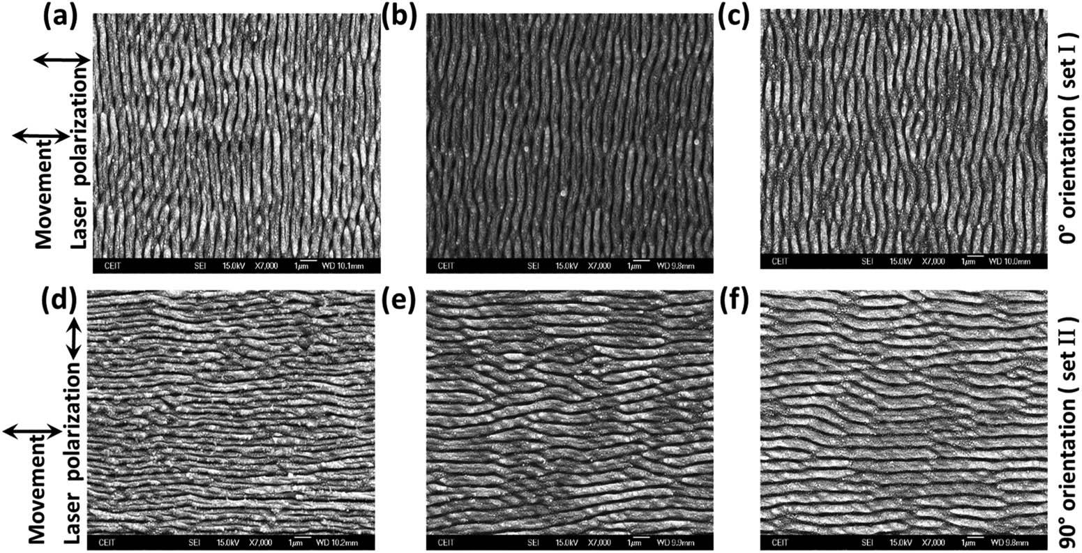
    Fig. 1. SEM images for quasi-sinusoidal LIPSS fabricated on top of a steel substrate using femtosecond laser processing. The polarization state of the laser beam is parallel to the direction of the movement during the sample processing for (a)–(c) subplots and perpendicular for (d)–(f).
    (a) AFM image and profile for the sample with period P=631 nm from set I. (b) AFM image and profile for the sample with period P=606 nm from set II.
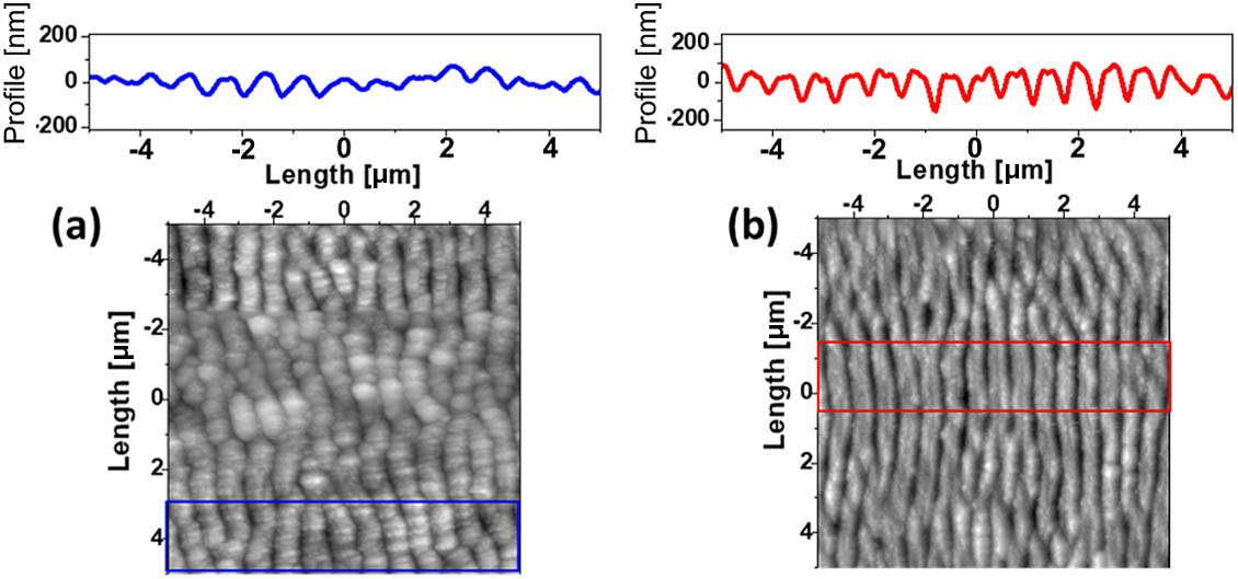
    Fig. 2. (a) AFM image and profile for the sample with period P=631  nm from set I. (b) AFM image and profile for the sample with period P=606  nm from set II.
    Subwavelength gratings studied: (a) sinusoidal and (b) binary. They have a period P=632 nm and are made of stainless steel. (c) Transversal sections showing the geometrical parameters of the profiles. In subplot (a), we have included a graphic layout showing the vector and components of the incoming electric field E, the azimuth angle φ (in our case φ=45°), the wavevector k, and the XYZ coordinate system. Note that the incidence angle is α=0° and it is not represented.
    Fig. 3. Subwavelength gratings studied: (a) sinusoidal and (b) binary. They have a period P=632  nm and are made of stainless steel. (c) Transversal sections showing the geometrical parameters of the profiles. In subplot (a), we have included a graphic layout showing the vector and components of the incoming electric field E, the azimuth angle φ (in our case φ=45°), the wavevector k, and the XYZ coordinate system. Note that the incidence angle is α=0° and it is not represented.
    Fitting of the simulated (solid lines) and experimentally measured (symbols) Stokes parameters for samples fabricated using femtosecond laser ablation with polarization (a) parallel and (b) perpendicular to the direction of the movement during the sample fabrication. (c)–(f) Plots show the geometrical parameters GH and β of the profile that best fit the experimental data for the two sets of samples [set I in (c) and (e), and set II in (d) and (f)]. The dashed red circles select the lowest β value on plot (e), and the highest β value on plot (f). The solid lines in plots (c)–(f) represent the cubic polynomial fitting of the geometrical parameters versus P.
    Fig. 4. Fitting of the simulated (solid lines) and experimentally measured (symbols) Stokes parameters for samples fabricated using femtosecond laser ablation with polarization (a) parallel and (b) perpendicular to the direction of the movement during the sample fabrication. (c)–(f) Plots show the geometrical parameters GH and β of the profile that best fit the experimental data for the two sets of samples [set I in (c) and (e), and set II in (d) and (f)]. The dashed red circles select the lowest β value on plot (e), and the highest β value on plot (f). The solid lines in plots (c)–(f) represent the cubic polynomial fitting of the geometrical parameters versus P.
    Maps of the normalized Stokes parameters q, u, and v, and reflectance R, as a function of the geometrical parameters GH and BW for the binary (left) and sinusoidal (right) gratings. The maximum value of reflectivity Rmax=0.6 is around the reflectivity value given by a regular, not nanostructured, stainless steel surface.
    Fig. 5. Maps of the normalized Stokes parameters q, u, and v, and reflectance R, as a function of the geometrical parameters GH and BW for the binary (left) and sinusoidal (right) gratings. The maximum value of reflectivity Rmax=0.6 is around the reflectivity value given by a regular, not nanostructured, stainless steel surface.
    Maps of the azimuth Ψ and ellipticity χ angles as a function of BW and GH parameters for the binary (left column) and sinusoidal (right column) profiles. The contour lines in the azimuth maps represent the values of Ψ=45° (in magenta), Ψ=−45°=135° (in cyan), and Ψ=0° and Ψ=180° (in yellow). The black contour lines in the ellipticity maps are for a value χ=0°. The locations of the configurations with χ=−45° and χ=+45° are given as white dots in the blue and red regions, respectively.
    Fig. 6. Maps of the azimuth Ψ and ellipticity χ angles as a function of BW and GH parameters for the binary (left column) and sinusoidal (right column) profiles. The contour lines in the azimuth maps represent the values of Ψ=45° (in magenta), Ψ=45°=135° (in cyan), and Ψ=0° and Ψ=180° (in yellow). The black contour lines in the ellipticity maps are for a value χ=0°. The locations of the configurations with χ=45° and χ=+45° are given as white dots in the blue and red regions, respectively.
    Full-wave propagation of the electric field on LIPSS for (a), (c), (e) binary grating, and (b), (d), (f) sinusoidal grating. The yellow arrows in (a) define the location of the source, LIPSS, reflection, and PML. The electric field in subplot (c) is linearly polarized and oriented along the 45° direction, being the point of view of the graphical representation almost coincident with the direction of the electric field vector. The labels for each field representation correspond to the cases presented in Table 1 and Fig. 5. We have also plotted the electric field distributions, along with the field evolution at the output, to help to understand the physical mechanism involved in the conversion.
    Fig. 7. Full-wave propagation of the electric field on LIPSS for (a), (c), (e) binary grating, and (b), (d), (f) sinusoidal grating. The yellow arrows in (a) define the location of the source, LIPSS, reflection, and PML. The electric field in subplot (c) is linearly polarized and oriented along the 45° direction, being the point of view of the graphical representation almost coincident with the direction of the electric field vector. The labels for each field representation correspond to the cases presented in Table 1 and Fig. 5. We have also plotted the electric field distributions, along with the field evolution at the output, to help to understand the physical mechanism involved in the conversion.
    Maps of the modulus of the elements of the Jones matrix |Pxx| and |Pyy|, and the relative phase shift between the electric field components of the reflected wave ϕ, in terms of the geometrical parameters GH and BW. The left column is for the binary profile and the right column is for the sinusoidal shape. The yellow line in the phase map corresponds to the configuration that shows an equal value of the modulus of the diagonal elements of the Jones matrix. The dots are the locations on the Pxx=Pyy line, where ϕ=±π/2; i.e., the geometries for CP. These dots coincide with those presented in Figs. 6(c) and 6(d).
    Fig. 8. Maps of the modulus of the elements of the Jones matrix |Pxx| and |Pyy|, and the relative phase shift between the electric field components of the reflected wave ϕ, in terms of the geometrical parameters GH and BW. The left column is for the binary profile and the right column is for the sinusoidal shape. The yellow line in the phase map corresponds to the configuration that shows an equal value of the modulus of the diagonal elements of the Jones matrix. The dots are the locations on the Pxx=Pyy line, where ϕ=±π/2; i.e., the geometries for CP. These dots coincide with those presented in Figs. 6(c) and 6(d).
    Binary LabelGH, BW [nm]R [%]Pol. StateSinusoidal LabelGH, BW [nm]R [%]Pol. State
    BqI880, 2751290° LPSqI905, 6152390° LP
    BqII500, 30019.390° LPSqII570, 62017.690° LP
    BqIII110, 3752890° LPSqIII220, 62531.190° LP
    BqIV615, 210180° LPSqIV800, 35014.50° LP
    BuI985, 20016 +45° LPSuI995, 44515.845° LP
    BuII580, 25018.3 +45° LPSuII770, 44017.5 +45° LP
    BuIII245, 18523.3 +45° LPSuIII600, 3603945° LP
    BuIV500, 22010.245° LPSuIV340, 29559 +45° LP
    BuV940, 12010.245° LP
    BvI640, 31037.3RCPSvI930, 4208.7RCP
    BvII250, 31545.5RCPSvII675, 40018.7LCP
    BvIII540, 2258.7LCPSvIII460, 38032.2RCP
    BvIV975, 15512.4LCPSvIV240, 16546LCP
    BvV200, 9545.6LCP
    Table 1. Geometrical Parameters and Reflectance of the Selected Minima and Maxima for the Binary and Sinusoidal Profilesa
    Mahmoud H. Elshorbagy, Luis Miguel Sánchez-Brea, Jerónimo Buencuerpo, Jesús del Hoyo, Ángela Soria-García, Verónica Pastor-Villarrubia, Alejandro San-Blas, Ainara Rodríguez, Santiago Miguel Olaizola, Javier Alda. Polarization conversion using customized subwavelength laser-induced periodic surface structures on stainless steel[J]. Photonics Research, 2022, 10(9): 2024
    Download Citation