
Mahmoud H. Elshorbagy, Luis Miguel Sánchez-Brea, Jerónimo Buencuerpo, Jesús del Hoyo, Ángela Soria-García, Verónica Pastor-Villarrubia, Alejandro San-Blas, Ainara Rodríguez, Santiago Miguel Olaizola, Javier Alda, "Polarization conversion using customized subwavelength laser-induced periodic surface structures on stainless steel," Photonics Res. 10, 2024 (2022)
- Photonics Research
- Vol. 10, Issue 9, 2024 (2022)
Abstract
1. INTRODUCTION
The state of polarization of light changes when interacting with anisotropic optical materials. In nature, this capability mostly relies on their atomic/molecular distribution that shows an anisotropy related to their crystalline characteristics [1–4]. Nanostructuring isotropic materials make it possible to tailor their optical response, allowing selective transmission, reflection, or absorption as a function of wavelength, the angle of incidence, and state of polarization [5,6]. In particular, subwavelength metallic gratings excite surface plasmon resonances using obliquely incident light, or cavity resonances at normal incidence [7]. Their use as filters to customize the balance between transmission, reflection, and absorption has been also demonstrated in waveguides and biosensors [7–14]. Regarding materials, silver is selected when looking for a sharp optical response, and gold is preferred in terms of its robustness against environmental agents, and its biocompatibility [11,15,16]. In addition, subwavelength structures in steel have been proposed for applications such as low-cost plasmonic devices [17–19] and the fabrication of colored surfaces [20]. Nanopatterned steel substrates also are used as templates to fabricate other nanostructured surfaces [21] or are directly included in optical systems [22]. However, the capabilities of nanostructured stainless steel for the modification of the polarization state of light still require further research to integrate them into low-cost optical systems. A relevant issue in the practical deployment of these devices is related to the existence of fast and efficient fabrication methods. Typically, electron beam lithography, deep UV lithography, focused ion beam, and nanoimprinting, combined with a number of deposition techniques (sputtering, spin coating, and thermal evaporation, for example), are common tools used to fabricate subwavelength structures [23]. As an alternative to generate subwavelength gratings, we used ultrafast laser processing to produce a laser-induced periodic surface structure (LIPSS) [24]. Besides the large throughput and low cost, an additional advantage of an LIPSS is that the nanostructure is created directly on the surface without postprocessing. The localized nanostructure is generated using pulses with a duration shorter than the thermal relaxation time of the material. This prevents energy that would modify the surrounding areas. The technique has been demonstrated for laser pulses lasting from femtoseconds to picoseconds [25]. However, the fabrication process requires an optimization of the multipulse delivery and a spatial control of the irradiated area [26]. This technique has been applied on metals [27,28], semiconductors [29,30], dielectrics [31], and thin films [32], indicating its high flexibility and effectiveness.
In this work, we study the optical properties of metallic nanostructures fabricated on stainless steel substrates. The nanostructures studied here present binary and sinusoidal profiles, and are generated by femtosecond laser processing. In Section 2, we have tuned the parameters of the sinusoidal profile to fit the simulated Stokes parameters to the experimental values. Section 3 presents the results of the Stokes vectors, Jones matrices, field distribution, and reflectance for binary and sinusoidal profiles in terms of their geometries. The obtained results indicate the possibility of using stainless steel as a promising material to fabricate nanostructured optical components that fulfill both cost and performance terms. Finally, Section 4 summarizes the main findings of this work.
2. FABRICATION, MODELING, AND VALIDATION
Our LIPSS is fabricated on top of AISI-304 stainless steel substrates (
Sign up for Photonics Research TOC. Get the latest issue of Photonics Research delivered right to you!Sign up now
Samples with different periods (from 590 nm to 635 nm) were fabricated for sets I and II. The mean height of the structures is kept constant at the profile height
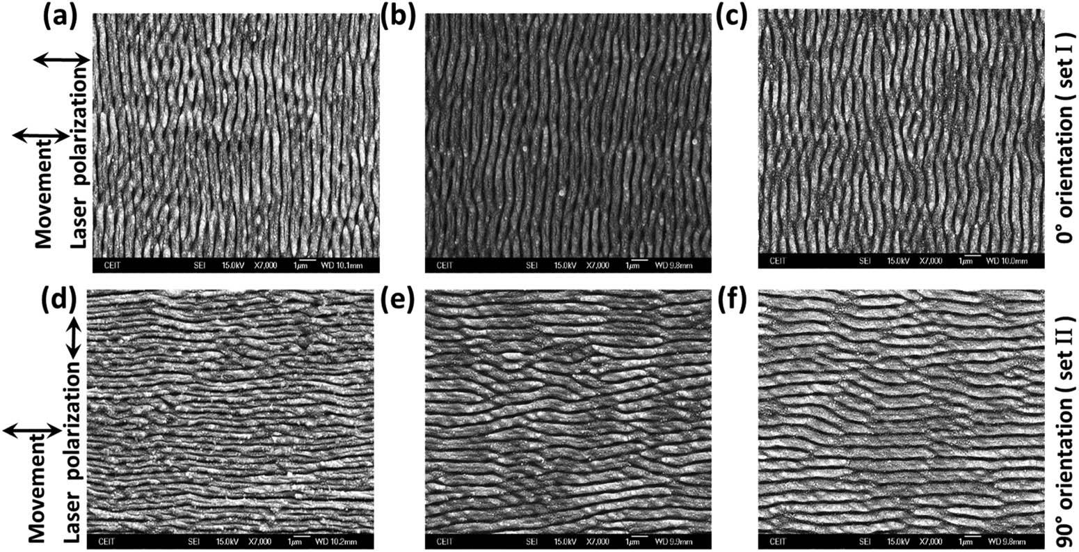
Figure 1.SEM images for quasi-sinusoidal LIPSS fabricated on top of a steel substrate using femtosecond laser processing. The polarization state of the laser beam is parallel to the direction of the movement during the sample processing for (a)–(c) subplots and perpendicular for (d)–(f).
![]()
Figure 2.(a) AFM image and profile for the sample with period
The profile is strongly dependent on the material of the sample, the conditions of the surface [34–37], and even on the substrate temperature [38,39]. This means that this profile departs from the ideal sinusoidal form. To accurately fit the simulated results of the optical polarization parameters with the experimental values, we need to take this deformation into account by introducing the profile function
![]()
Figure 3.Subwavelength gratings studied: (a) sinusoidal and (b) binary. They have a period
Our model uses a plane wave impinging perpendicularly on the substrate, which is
This analysis uses the Stokes vector to describe the state of polarization of the reflected light
The Stokes parameters of the light reflected by the fabricated structures were measured using an illumination spot of around 2 mm in diameter. The light source was a He–Ne laser [model 1122P, JDS Uniphase (JDSU), which is now VIAVI Solutions] emitting at
The electric field distributions evaluated by the COMSOL software are used to calculate the Stokes parameters of the reflected light [33,40]. For each sample, the matching between experimental and simulated Stokes parameters is obtained individually by changing the geometry of the grating in terms of its height, GH, and shape
![]()
Figure 4.Fitting of the simulated (solid lines) and experimentally measured (symbols) Stokes parameters for samples fabricated using femtosecond laser ablation with polarization (a) parallel and (b) perpendicular to the direction of the movement during the sample fabrication. (c)–(f) Plots show the geometrical parameters GH and
The values of GH producing a best fitting are presented in Figs. 4(c), and 4(d), for sets I and II, respectively. The mean heights for sets I and II are
3. POLARIZATION MODULATION WITH BINARY AND SINUSOIDAL GRATINGS
To better understand the effect of the geometry of our LIPSS on the modification of the polarization state, besides the sinusoidal profile, we extend our calculations to binary gratings. These binary shapes are parameterized by the height of the profile, GH, and the width of the base, BW. In this section, we focus on how these geometrical parameters change the polarization state of the incoming light. We fix the period in both structures to
Figure 5 represents the normalized Stokes parameters
![]()
Figure 5.Maps of the normalized Stokes parameters
To have them properly identified, we label them with a capital letter: B for binary (rectangular) and
Geometrical Parameters and Reflectance of the Selected Minima and Maxima for the Binary and Sinusoidal Profiles
| Binary Label | GH, BW [nm] | Pol. State | Sinusoidal Label | GH, BW [nm] | Pol. State | ||
|---|---|---|---|---|---|---|---|
| 880, 275 | 12 | 90° LP | 905, 615 | 23 | 90° LP | ||
| 500, 300 | 19.3 | 90° LP | 570, 620 | 17.6 | 90° LP | ||
| 110, 375 | 28 | 90° LP | 220, 625 | 31.1 | 90° LP | ||
| 615, 210 | 18 | 0° LP | 800, 350 | 14.5 | 0° LP | ||
| 985, 200 | 16 | | 995, 445 | 15.8 | |||
| 580, 250 | 18.3 | | 770, 440 | 17.5 | | ||
| 245, 185 | 23.3 | | 600, 360 | 39 | |||
| 500, 220 | 10.2 | 340, 295 | 59 | | |||
| 940, 120 | 10.2 | ||||||
| 640, 310 | 37.3 | RCP | 930, 420 | 8.7 | RCP | ||
| 250, 315 | 45.5 | RCP | 675, 400 | 18.7 | LCP | ||
| 540, 225 | 8.7 | LCP | 460, 380 | 32.2 | RCP | ||
| 975, 155 | 12.4 | LCP | 240, 165 | 46 | LCP | ||
| 200, 95 | 45.6 | LCP |
The state of polarization of the reflected light is given in the Pol. State column.
The identification of the maxima and minima in the maps of the Stokes parameters makes it possible to select geometrical parameters of the grating that generate a well-defined state of polarization. The maximum
For the generated light states, we also calculated the azimuth angle
Azimuth directly represents the rotation angle of the axis of the polarization ellipse, allowing easy identification of the horizontal (
![]()
Figure 6.Maps of the azimuth
The physical mechanisms of the polarization conversion may involve the selective absorption of the field components, and/or additional phase shifts between them. The input field components generate surface currents circulating the structure. Depending on the topography, these currents can be attenuated through Joule dissipation or plasmonic resonances, or they can emit electromagnetic waves with a phase difference between components that is strongly dependent on the geometry. The change in the polarization state can be visualized using 3D plots of the fields obtained by a full wave analysis of the structure during the propagation process. The results of this analysis are shown in Fig. 7 for the binary grating on the left, and sinusoidal on the right plots. The plots use a selection of some points in Table 1 to show representative polarization conversion using the binary or sinusoidal gratings. In Fig. 7(a), the locations of the source, LIPSS, reflected light, and PML domains are shown using yellow arrows. The reflected light can be axial LP, as in Figs. 7(a) and 7(b), or
![]()
Figure 7.Full-wave propagation of the electric field on LIPSS for (a), (c), (e) binary grating, and (b), (d), (f) sinusoidal grating. The yellow arrows in (a) define the location of the source, LIPSS, reflection, and PML. The electric field in subplot (c) is linearly polarized and oriented along the 45° direction, being the point of view of the graphical representation almost coincident with the direction of the electric field vector. The labels for each field representation correspond to the cases presented in Table
The previous analysis is a particular case for just one incident illumination: 45° linearly polarized light. However, to totally characterize the polarimetric properties of the LIPSS, the polarization matrix of the material must be calculated. Since we assume that an LIPSS is periodical, depolarization analysis is not required, so we can use the Jones formalism. Mathematically, this is written as
In our case, the grating generated as an LIPSS can be described by the corresponding Jones matrix
Then, it is possible to obtain the two nonzero elements of the Jones matrix by just comparing the input and output electric field components:
The reflectance of the LIPSS also can be calculated as
Finally, we calculated these parameters from the simulations shown previously. Figure 8 represents the modulus of
![]()
Figure 8.Maps of the modulus of the elements of the Jones matrix
4. CONCLUSIONS
We show how a fabricated stainless steel LIPSS can produce a change in the state of polarization of an incoming radiation under normal incidence conditions. The Stokes parameters of several experimental samples with different periods and heights have been measured. These results have been compared to simulations obtained from computational electromagnetism. The shape of the LIPSS has been tuned to match the simulations to the experimental results. The resulting parameters for the fitting are in accordance with the experimental profiles derived from the SEM and AFM images.
Once the simulation conditions were validated, we made a detailed analysis of the LIPSS geometry for binary and sinusoidal shapes to find those configurations that generate a significant variation of the state of polarization of the incoming light. By controlling the steel nanostructure geometry, we can tune the polarization characteristics. These devices can act as wave retarders or linear polarizers. In fact, we have demonstrated that a customized profile of an LIPSS can generate any polarization state when illuminated by a linearly polarized beam having an azimuth of 45°. To summarize, we conclude that the analysis made here can promote the use of an LIPSS on stainless steel to fabricate low-cost retarders and polarization filters.
References
[1] Y. P. Svirko, N. I. Zheludev. Polarization of Light in Nonlinear Optics(2000).
[2] D. F. Eaton. Nonlinear optical materials. Science, 253, 281-287(1991).
[3] V. Lucarini, J. J. Saarinen, K.-E. Peiponen, E. M. Vartiainen. Kramers-Kronig Relations in Optical Materials Research, 110(2005).
[4] M. K. Chen, Y. Wu, L. Feng, Q. Fan, M. Lu, T. Xu, D. P. Tsai. Principles, functions, and applications of optical meta-lens. Adv. Opt. Mater., 9, 2001414(2021).
[5] M. B. Ross, C. A. Mirkin, G. C. Schatz. Optical properties of one-, two-, and three-dimensional arrays of plasmonic nanostructures. J. Phys. Chem. C, 120, 816-830(2016).
[6] J. Alda, G. D. Boreman. Infrared Antennas and Resonant Structures(2017).
[7] J. Zhou, L. J. Guo. Transition from a spectrum filter to a polarizer in a metallic nano-slit array. Sci. Rep., 4, 3614(2014).
[8] L. Wang, Z. Zhang. Resonance transmission or absorption in deep gratings explained by magnetic polaritons. Appl. Phys. Lett., 95, 111904(2009).
[9] C. Han, W. Y. Tam. Plasmonic ultra-broadband polarizers based on Ag nano wire-slit arrays. Appl. Phys. Lett., 106, 081102(2015).
[10] C. Lertvachirapaiboon, A. Baba, S. Ekgasit, K. Shinbo, K. Kato, F. Kaneko. Transmission surface plasmon resonance techniques and their potential biosensor applications. Biosens. Bioelectron., 99, 399-415(2018).
[11] A. Polyakov, K. Thompson, S. Dhuey, D. Olynick, S. Cabrini, P. Schuck, H. Padmore. Plasmon resonance tuning in metallic nanocavities. Sci. Rep., 2, 933(2012).
[12] M. Vincenti, D. de Ceglia, M. Grande, A. D’Orazio, M. Scalora. Tailoring absorption in metal gratings with resonant ultrathin bridges. Plasmonics, 8, 1445-1456(2013).
[13] H. Yan, L. Huang, X. Xu, S. Chakravarty, N. Tang, H. Tian, R. T. Chen. Unique surface sensing property and enhanced sensitivity in microring resonator biosensors based on subwavelength grating waveguides. Opt. Express, 24, 29724-29733(2016).
[14] N. Kazanskiy, M. Butt, S. Khonina. Silicon photonic devices realized on refractive index engineered subwavelength grating waveguides-a review. Opt. Laser Technol., 138, 106863(2021).
[15] P. Dong, Y. Wu, W. Guo, J. Di. Plasmonic biosensor based on triangular Au/Ag and Au/Ag/Au core/shell nanoprisms onto indium tin oxide glass. Plasmonics, 8, 1577-1583(2013).
[16] D. V. Nesterenko, Z. Sekkat. Resolution estimation of the Au, Ag, Cu, and Al single-and double-layer surface plasmon sensors in the ultraviolet, visible, and infrared regions. Plasmonics, 8, 1585-1595(2013).
[17] P. R. West, S. Ishii, G. V. Naik, N. K. Emani, V. M. Shalaev, A. Boltasseva. Searching for better plasmonic materials. Laser Photon. Rev., 4, 795-808(2010).
[18] L. Polavarapu, L. M. Liz-Marzán. Towards low-cost flexible substrates for nanoplasmonic sensing. Phys. Chem. Chem. Phys., 15, 5288-5300(2013).
[19] M. Seo, J. Lee, M. Lee. Grating-coupled surface plasmon resonance on bulk stainless steel. Opt. Express, 25, 26939-26949(2017).
[20] M. S. Ahsan, F. Ahmed, Y. G. Kim, M. S. Lee, M. B. Jun. Colorizing stainless steel surface by femtosecond laser induced micro/nano-structures. Appl. Surf. Sci., 257, 7771-7777(2011).
[21] T.-F. Yao, P.-H. Wu, T.-M. Wu, C.-W. Cheng, S.-Y. Yang. Fabrication of anti-reflective structures using hot embossing with a stainless steel template irradiated by femtosecond laser. Microelectron. Eng., 88, 2908-2912(2011).
[22] P. Boillot, J. Peultier. Use of stainless steels in the industry: recent and future developments. Proc. Eng., 83, 309-321(2014).
[23] L. Chi. Nanotechnology, 8(2010).
[24] J. Bonse, A. Rosenfeld, J. Krüger. On the role of surface plasmon polaritons in the formation of laser-induced periodic surface structures upon irradiation of silicon by femtosecond-laser pulses. J. Appl. Phys., 106, 104910(2009).
[25] A. Y. Vorobyev, C. Guo. Direct femtosecond laser surface nano/microstructuring and its applications. Laser Photon. Rev., 7, 385-407(2013).
[26] M. Birnbaum. Semiconductor surface damage produced by ruby lasers. J. Appl. Phys., 36, 3688-3689(1965).
[27] M. J. Cherukara, K. Sasikumar, A. DiChiara, S. J. Leake, W. Cha, E. M. Dufresne, T. Peterka, I. McNulty, D. A. Walko, H. Wen, S. J. R. S. Sankaranarayanan, R. J. Harder. Ultrafast three-dimensional integrated imaging of strain in core/shell semiconductor/metal nanostructures. Nano Lett., 17, 7696-7701(2017).
[28] C. Byram, S. S. B. Moram, A. K. Shaik, V. R. Soma. Versatile gold based SERS substrates fabricated by ultrafast laser ablation for sensing picric acid and ammonium nitrate. Chem. Phys. Lett., 685, 103-107(2017).
[29] A. Y. Zhizhchenko, P. Tonkaev, D. Gets, A. Larin, D. Zuev, S. Starikov, E. V. Pustovalov, A. M. Zakharenko, S. A. Kulinich, S. Juodkazis, A. A. Kuchmizhak, S. V. Makarov. Light-emitting nanophotonic designs enabled by ultrafast laser processing of halide perovskites. Small, 16, 2000410(2020).
[30] M. Sanz, M. Lopez-Arias, J. F. Marco, R. de Nalda, S. Amoruso, G. Ausanio, S. Lettieri, R. Bruzzese, X. Wang, M. Castillejo. Ultrafast laser ablation and deposition of wide band gap semiconductors. J. Phys. Chem. C, 115, 3203-3211(2011).
[31] A. Rudenko, J.-P. Colombier, S. Höhm, A. Rosenfeld, J. Krüger, J. Bonse, T. E. Itina. Spontaneous periodic ordering on the surface and in the bulk of dielectrics irradiated by ultrafast laser: a shared electromagnetic origin. Sci. Rep., 7, 12306(2017).
[32] A. Cerkauskaite, R. Drevinskas, A. Solodar, I. Abdulhalim, P. G. Kazansky. Form-birefringence in ITO thin films engineered by ultrafast laser nanostructuring. ACS Photon., 4, 2944-2951(2017).
[33] A. San-Blas, M. Martinez-Calderon, J. Buencuerpo, L. M. Sanchez-Brea, J. Del Hoyo, M. Gómez-Aranzadi, A. Rodríguez, S. Olaizola. Femtosecond laser fabrication of LIPSS-based waveplates on metallic surfaces. Appl. Surf. Sci., 520, 146328(2020).
[34] J. Sipe, J. F. Young, J. Preston, H. Van Driel. Laser-induced periodic surface structure. I. Theory. Phys. Rev. B, 27, 1141-1154(1983).
[35] A. Vorobyev, C. Guo. Enhanced absorptance of gold following multipulse femtosecond laser ablation. Phys. Rev. B, 72, 195422(2005).
[36] C. Florian, S. V. Kirner, J. Krüger, J. Bonse. Surface functionalization by laser-induced periodic surface structures. J. Laser Appl., 32, 022063(2020).
[37] M. Prudent, F. Bourquard, A. Borroto, J.-F. Pierson, F. Garrelie, J.-P. Colombier. Initial morphology and feedback effects on laser-induced periodic nanostructuring of thin-film metallic glasses. Nanomaterials, 11, 1076(2021).
[38] S. Gräf, C. Kunz, S. Engel, T. J.-Y. Derrien, F. A. Müller. Femtosecond laser-induced periodic surface structures on fused silica: the impact of the initial substrate temperature. Materials, 11, 1340(2018).
[39] Q. Li, Q. Wu, Y. Li, C. Zhang, Z. Jia, J. Yao, J. Sun, J. Xu. Femtosecond laser-induced periodic surface structures on lithium niobate crystal benefiting from sample heating. Photon. Res., 6, 789-793(2018).
[40] E. Collett. Field Guide to Polarization(2005).
[41] E. Skoulas, A. Manousaki, C. Fotakis, E. Stratakis. Biomimetic surface structuring using cylindrical vector femtosecond laser beams. Sci. Rep., 7, 45114(2017).
[42] N. Livakas, E. Skoulas, E. Stratakis. Omnidirectional iridescence via cylindrically-polarized femtosecond laser processing. Opto-Electron. Adv., 3, 190035(2020).
[43] H. W. Siesler, Y. Ozaki, S. Kawata, H. M. Heise. Near-infrared Spectroscopy: Principles, Instruments, Applications(2008).


Set citation alerts for the article
Please enter your email address

© Copyright 2018-2021 | Chinese Laser Press. All Rights Reserved 沪ICP备15018463号-20