• Journal of Semiconductors
  • Vol. 41, Issue 7, 071901 (2020)
Peng Zhang1, Yiwei Zhang1, Yi Wei2, Huaning Jiang1, Xingguo Wang1, and Yongji Gong1
Author Affiliations
  • 1School of Materials Science and Engineering, Beihang University, Beijing 100191, China
  • 2State Key Laboratory of Organic–Inorganic Composites, Beijing Key Laboratory of Electrochemical Process and Technology for Materials, Beijing University of Chemical Technology, Beijing 100029 China
  • show less
    DOI: 10.1088/1674-4926/41/7/071901 Cite this Article
    Peng Zhang, Yiwei Zhang, Yi Wei, Huaning Jiang, Xingguo Wang, Yongji Gong. Contact engineering for two-dimensional semiconductors[J]. Journal of Semiconductors, 2020, 41(7): 071901 Copy Citation Text show less
    (Color online) Atomic structure of representative 2D semiconductor materials and phase engineered contacts. (a, b) Top and side view of 2H stacked structure of 2D semiconductor. (c) Device model of 2D SCs based device. (d–f) Different types of metal–semiconductor junction with contact interface.
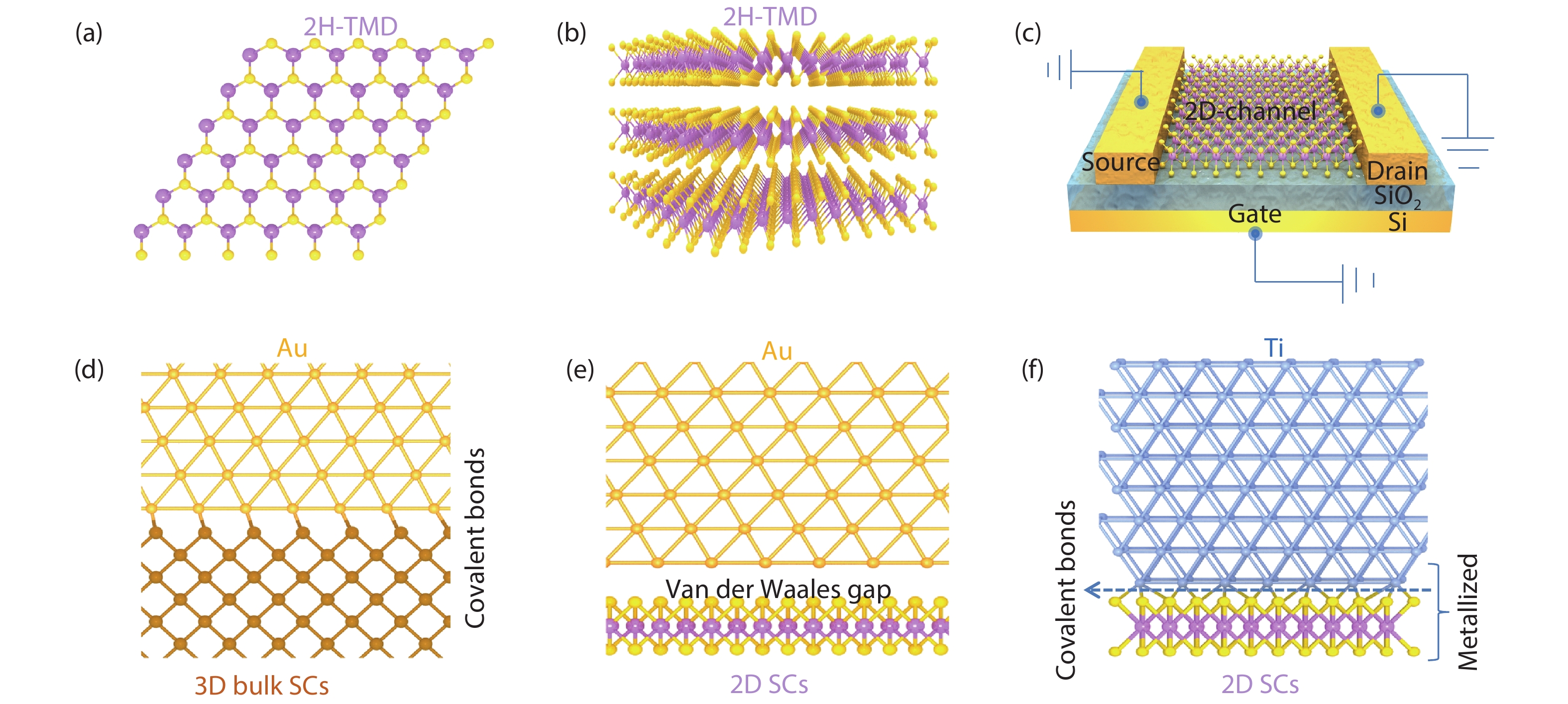
    Fig. 1. (Color online) Atomic structure of representative 2D semiconductor materials and phase engineered contacts. (a, b) Top and side view of 2H stacked structure of 2D semiconductor. (c) Device model of 2D SCs based device. (d–f) Different types of metal–semiconductor junction with contact interface.
    (Color online) (a, b) 3D top contact and 3D edge contact configuration of metal-2D SCs contact. (c, d) 2D top contact and 2D edge contact of metallic 2D-SCs contact geometries.
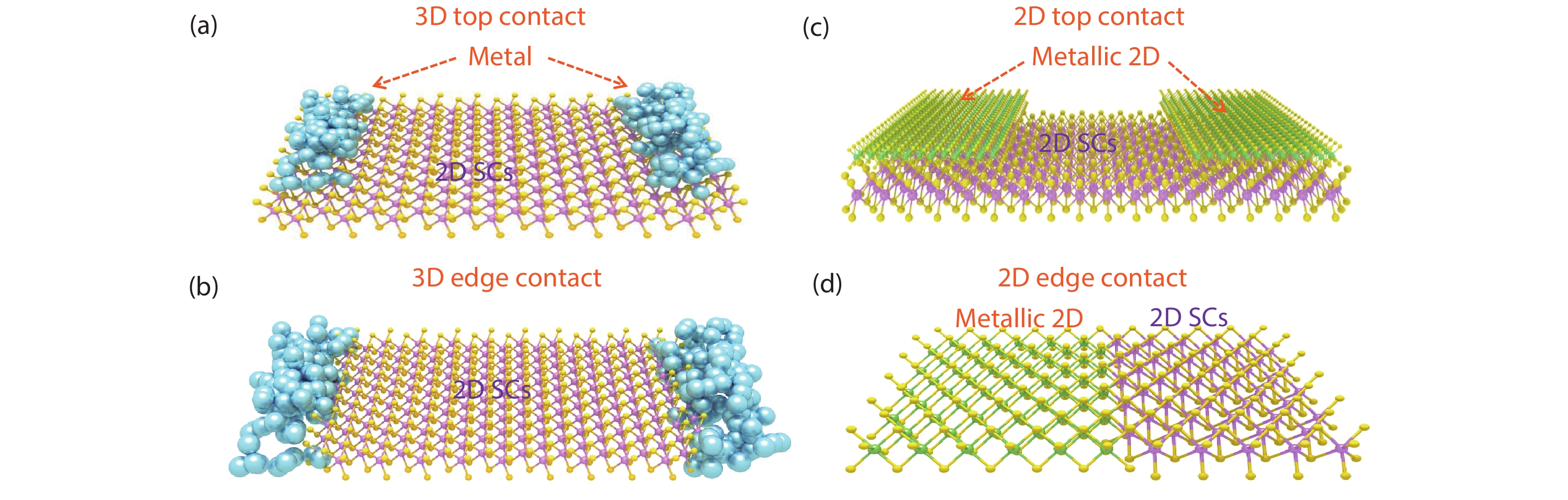
    Fig. 2. (Color online) (a, b) 3D top contact and 3D edge contact configuration of metal-2D SCs contact. (c, d) 2D top contact and 2D edge contact of metallic 2D-SCs contact geometries.
    (Color online) Schematic diagram of a conventional Si-based NMOS FET.
    Fig. 3. (Color online) Schematic diagram of a conventional Si-based NMOS FET.
    (Color online) (a) Schematic diagram of various metal–MoS2 band alignments along with work function of metal (ФM). The Fermi level of metal is lined up close to conduction band of MoS2. The left-hand part in Fig. 4(a) is the actual ФSB extracted from experiment, which is different from the theoretical value calculated by the difference of ФM (right-hand part in Fig. 4(a)) and electron affinity (χ) of MoS2. For example, theoretical values of ФSB for Sc–MoS2 and Pt–MoS2 contact are about –0.7 and 1.4 eV, respectively. However, the actual ФSB obtained from experiment is only 30 and 230 meV, indicating that there is a strong Fermi level pinning effect at the interface of metal and 2D SCs. (b) Energy band diagrams of MoS2 with and without 2D metallic materials.
    Fig. 4. (Color online) (a) Schematic diagram of various metal–MoS2 band alignments along with work function of metal (ФM). The Fermi level of metal is lined up close to conduction band of MoS2. The left-hand part in Fig. 4(a) is the actual ФSB extracted from experiment, which is different from the theoretical value calculated by the difference of ФM (right-hand part in Fig. 4(a)) and electron affinity (χ) of MoS2. For example, theoretical values of ФSB for Sc–MoS2 and Pt–MoS2 contact are about –0.7 and 1.4 eV, respectively. However, the actual ФSB obtained from experiment is only 30 and 230 meV, indicating that there is a strong Fermi level pinning effect at the interface of metal and 2D SCs. (b) Energy band diagrams of MoS2 with and without 2D metallic materials.
    (Color online) Metal contact investigation of MoS2 device. (a) Schematic diagram of back gated MoS2 transistor. (b, c) SEM and AFM images of device with MoS2 thickness of 3 nm. (d) The expected position of the metal Fermi level across the band of MoS2, where the ФSB was decided by the Schottky–Mott rule. (e) Transfer characteristics of MoS2 device with different contact metal. The inset is the actual position of Fermi level of from experimental date. (f) Temperature-dependent transfer curves with Ni contact, where the contribution of thermionic emission and thermally assisted tunneling are marked. (g) Arrhenius-type plot from (a). (h) Extracted actual ФSB for Ni-contacted MoS2 device. (i) The relationship of ФSB with metal work function[86]. Copyright 2013, American Chemical Society.
    Fig. 5. (Color online) Metal contact investigation of MoS2 device. (a) Schematic diagram of back gated MoS2 transistor. (b, c) SEM and AFM images of device with MoS2 thickness of 3 nm. (d) The expected position of the metal Fermi level across the band of MoS2, where the ФSB was decided by the Schottky–Mott rule. (e) Transfer characteristics of MoS2 device with different contact metal. The inset is the actual position of Fermi level of from experimental date. (f) Temperature-dependent transfer curves with Ni contact, where the contribution of thermionic emission and thermally assisted tunneling are marked. (g) Arrhenius-type plot from (a). (h) Extracted actual ФSB for Ni-contacted MoS2 device. (i) The relationship of ФSB with metal work function[86]. Copyright 2013, American Chemical Society.
    (Color online) In contacted MoS2 transistors. (a) Device mode of MoS2 based back-gated device. The electrodes consist of 10 nm In layer capped with 100 nm Au. (b) Cross-sectional annular dark field (ADF) scanning transmission electron microscopy (STEM) of interface of In-MoS2. (c, d) Extracted contact resistance using transmission line method for MoS2 with thickness of 0.7 and 8.1 nm, respectively. (e, f) Comparison of contact resistance versus carrier concentration with different contact materials from literatures. (g, h) Transfer characteristics of device with monolayer MoS2 and temperature-dependent transfer curves for 8 nm MoS2 device. (i) Output curves with linear relationship indicates ohmic contact. (j) Extracted ФSB with value of 110 meV, indicates the ideal contact between the interface of In and MoS2, which is nearly the same as the value decided by the Schottky–Mott rule. The inset is the energy band diagram of MoS2 and In[87]. Copyright 2019, Nature Publishing Group.
    Fig. 6. (Color online) In contacted MoS2 transistors. (a) Device mode of MoS2 based back-gated device. The electrodes consist of 10 nm In layer capped with 100 nm Au. (b) Cross-sectional annular dark field (ADF) scanning transmission electron microscopy (STEM) of interface of In-MoS2. (c, d) Extracted contact resistance using transmission line method for MoS2 with thickness of 0.7 and 8.1 nm, respectively. (e, f) Comparison of contact resistance versus carrier concentration with different contact materials from literatures. (g, h) Transfer characteristics of device with monolayer MoS2 and temperature-dependent transfer curves for 8 nm MoS2 device. (i) Output curves with linear relationship indicates ohmic contact. (j) Extracted ФSB with value of 110 meV, indicates the ideal contact between the interface of In and MoS2, which is nearly the same as the value decided by the Schottky–Mott rule. The inset is the energy band diagram of MoS2 and In[87]. Copyright 2019, Nature Publishing Group.
    (Color online) Transferred metal electrode contacted MoS2 FET. (a–c) Cross-sectional atomic mode and optical images of MoS2 device with transferred Au and the transferred Au mechanically released. (d–f) Cross-sectional schematics and optical images of MoS2 device with traditional electron-beam-deposited Au and the deposited Au mechanically released. (g, h) Cross-sectional schematics and TEM images of transferred and evaporated Au. (i, j) Transfer curves of MoS2 devices with different transferred and deposited metals. (k) Experimentally extracted ФSB for different transferred and evaporated metals[60]. Copyright 2018, Nature Publishing Group.
    Fig. 7. (Color online) Transferred metal electrode contacted MoS2 FET. (a–c) Cross-sectional atomic mode and optical images of MoS2 device with transferred Au and the transferred Au mechanically released. (d–f) Cross-sectional schematics and optical images of MoS2 device with traditional electron-beam-deposited Au and the deposited Au mechanically released. (g, h) Cross-sectional schematics and TEM images of transferred and evaporated Au. (i, j) Transfer curves of MoS2 devices with different transferred and deposited metals. (k) Experimentally extracted ФSB for different transferred and evaporated metals[60]. Copyright 2018, Nature Publishing Group.
    (Color online) Edge contact investigation of MoS2 device. (a) Schematic diagram of hBN encapsulated MoS2 device with graphene edge contact. (b–d) Temperature dependent output curves, contact resistance and temperature dependent Hall mobility, respectively[66]. Copyright 2016, Nature Publishing Group (e) Schematic of Al2O3 capped edge contacted MoS2 device. (f–h) Output curves, transfer characteristic and mobility with different drain voltage for Al2O3 capped MoS2 device. (i) Schematic of h-BN capped edge contacted MoS2 device. (j–l) Output curves, transfer characteristic and mobility with different drain voltage for hBN capped MoS2 device[67]. Copyright 2016, WILEY-VCH Verlag GmbH & Co. KGaA, Weinheim.
    Fig. 8. (Color online) Edge contact investigation of MoS2 device. (a) Schematic diagram of hBN encapsulated MoS2 device with graphene edge contact. (b–d) Temperature dependent output curves, contact resistance and temperature dependent Hall mobility, respectively[66]. Copyright 2016, Nature Publishing Group (e) Schematic of Al2O3 capped edge contacted MoS2 device. (f–h) Output curves, transfer characteristic and mobility with different drain voltage for Al2O3 capped MoS2 device. (i) Schematic of h-BN capped edge contacted MoS2 device. (j–l) Output curves, transfer characteristic and mobility with different drain voltage for hBN capped MoS2 device[67]. Copyright 2016, WILEY-VCH Verlag GmbH & Co. KGaA, Weinheim.
    (Color online) Contact engineering of vertical 2D metallic-2H WSe2 heterostructure. (a) Sequential growth scheme of vertical WSe2 and WT2 heterostructure. The inset is the optical images of WSe2 and WTe2. (b) Device mode of WSe2 with and without contact. (c, d) Output curves and temperature-dependent conductivity of WSe2 device with WTe2 and Ti contact. (e) Built-in potential energy versus back-gated voltage for Ti and WTe2 contacted WSe2 devices. (f) ФSB height with the function of metal work function[76]. Copyright 2013, American Chemical Society. (g, h) Atomic structure of van der Waals epitaxy growth of 2D metallic-SCs heterostructure and optical image of NbTe2-WSe2 heterostructure. (i, j) Schematic model of WSe2 device with NbTe2 and Ti contact. (k–n) Current–voltage and transfer characteristics of WSe2 device with and without NbTe2 contact. The inset is optical images of fabricated devices[77]. Copyright 2019, WILEY-VCH Verlag GmbH & Co. KGaA, Weinheim.
    Fig. 9. (Color online) Contact engineering of vertical 2D metallic-2H WSe2 heterostructure. (a) Sequential growth scheme of vertical WSe2 and WT2 heterostructure. The inset is the optical images of WSe2 and WTe2. (b) Device mode of WSe2 with and without contact. (c, d) Output curves and temperature-dependent conductivity of WSe2 device with WTe2 and Ti contact. (e) Built-in potential energy versus back-gated voltage for Ti and WTe2 contacted WSe2 devices. (f) ФSB height with the function of metal work function[76]. Copyright 2013, American Chemical Society. (g, h) Atomic structure of van der Waals epitaxy growth of 2D metallic-SCs heterostructure and optical image of NbTe2-WSe2 heterostructure. (i, j) Schematic model of WSe2 device with NbTe2 and Ti contact. (k–n) Current–voltage and transfer characteristics of WSe2 device with and without NbTe2 contact. The inset is optical images of fabricated devices[77]. Copyright 2019, WILEY-VCH Verlag GmbH & Co. KGaA, Weinheim.
    (Color online) Contact engineering of lateral graphene–MoS2 and VS2–MoS2 heterostructures. (a) Schematic diagram of MoS2–graphene lateral heterostructure. (b, c) Transfer and output curves of graphene contacted MoS2 device. (d) Statistics of obtained mobility from graphene contacted MoS2 device[91]. Copyright 2016, Nature Publishing Group. (e) Schematic fabrication of the MoS2–graphene lateral heterostructure. (f, g) Representative transfer and output curves of graphene contacted MoS2 deice. (h) Total, contact and channel resistance of graphene contacted MoS2 device[92]. Copyright 2016, WILEY-VCH Verlag GmbH & Co. KGaA, Weinheim. (i) Device schematic of VS 2 contacted MoS2. (j) Ids–Vds curves of MoS2 device with VS2 and Ni contact. (k) Extracted ФSB of VS2 and Ni contacted MoS2 as a function of Vbg. (l) Contact resistance of Ni and VS2 contacted MoS2 devices[75]. Copyright 2018, American Chemical Society.
    Fig. 10. (Color online) Contact engineering of lateral graphene–MoS2 and VS2–MoS2 heterostructures. (a) Schematic diagram of MoS2–graphene lateral heterostructure. (b, c) Transfer and output curves of graphene contacted MoS2 device. (d) Statistics of obtained mobility from graphene contacted MoS2 device[91]. Copyright 2016, Nature Publishing Group. (e) Schematic fabrication of the MoS2–graphene lateral heterostructure. (f, g) Representative transfer and output curves of graphene contacted MoS2 deice. (h) Total, contact and channel resistance of graphene contacted MoS2 device[92]. Copyright 2016, WILEY-VCH Verlag GmbH & Co. KGaA, Weinheim. (i) Device schematic of VS 2 contacted MoS2. (j) IdsVds curves of MoS2 device with VS2 and Ni contact. (k) Extracted ФSB of VS2 and Ni contacted MoS2 as a function of Vbg. (l) Contact resistance of Ni and VS2 contacted MoS2 devices[75]. Copyright 2018, American Chemical Society.
    (Color online) Electron donation, laser or Ar plasma induced metallic phase as contact. (a) Electrostatic force microscopy phase image of 1T–2H–1T lateral MoS2 heterostructure. (b–d) Resistance, output and transfer curves of 2H phase MoS2 with metallic 1T phase MoS2 contact. The inset is the device model of MoS2 device with Au and 1T metallic MoS2 contact[80]. Copyright 2014, Nature Publishing Group. Laser induced phase transition of metallic 1T’-MoTe2. (e) Atomic structure and laser treated process. (f) Device schematic with metallic 1T’-MoTe2 contact. (g) Output characteristic of MoTe2 device with 1T’-MoTe2 contact. (h) Field-effect mobility as a function of temperature of MoTe2 device with Au and metallic MoTe2 contact2 contact[80]. Copyright 2015, American Association for the Advancement of Science (AAAS). (i) Atomic structure and schematic representation of plasma-treated process. (j) Device models with Au or 1T/2H phase MoS2 contact. (k, l) Output and transfer curves with different Au and 1T/2H phase MoS2 contact[81]. Copyright 2017, American Chemical Society.
    Fig. 11. (Color online) Electron donation, laser or Ar plasma induced metallic phase as contact. (a) Electrostatic force microscopy phase image of 1T–2H–1T lateral MoS2 heterostructure. (b–d) Resistance, output and transfer curves of 2H phase MoS2 with metallic 1T phase MoS2 contact. The inset is the device model of MoS2 device with Au and 1T metallic MoS2 contact[80]. Copyright 2014, Nature Publishing Group. Laser induced phase transition of metallic 1T’-MoTe2. (e) Atomic structure and laser treated process. (f) Device schematic with metallic 1T’-MoTe2 contact. (g) Output characteristic of MoTe2 device with 1T’-MoTe2 contact. (h) Field-effect mobility as a function of temperature of MoTe2 device with Au and metallic MoTe2 contact2 contact[80]. Copyright 2015, American Association for the Advancement of Science (AAAS). (i) Atomic structure and schematic representation of plasma-treated process. (j) Device models with Au or 1T/2H phase MoS2 contact. (k, l) Output and transfer curves with different Au and 1T/2H phase MoS2 contact[81]. Copyright 2017, American Chemical Society.
    (Color online) Intercalation induced phase transition of SnS2. (a) and (b) Atomic structures of pristine SnS2, Cu and Co intercalated SnS2. (c–f) Optical images of pure SnS2, Cu, Co and Cu–Co intercalated SnS2. (g) Temperature-dependent resistance of SnS2, Cu–SnS2, Co–SnS2 and few layer graphene, where the Cu–SnS2 presents semiconductor behavior while the Co–SnS2 behaves as a metal like graphene. (h) Transfer curves of Cu–SnS2 with p-type characteristic. (i) I–V curves of Co–SnS2 contacted SnS2 and Cu–SnS2 devices. (j) SnS2/Cu–SnS2 junction with and without metallic Co–SnS2 contact[82]. Copyright 2018, Nature Publishing Group.
    Fig. 12. (Color online) Intercalation induced phase transition of SnS2. (a) and (b) Atomic structures of pristine SnS2, Cu and Co intercalated SnS2. (c–f) Optical images of pure SnS2, Cu, Co and Cu–Co intercalated SnS2. (g) Temperature-dependent resistance of SnS2, Cu–SnS2, Co–SnS2 and few layer graphene, where the Cu–SnS2 presents semiconductor behavior while the Co–SnS2 behaves as a metal like graphene. (h) Transfer curves of Cu–SnS2 with p-type characteristic. (i) IV curves of Co–SnS2 contacted SnS2 and Cu–SnS2 devices. (j) SnS2/Cu–SnS2 junction with and without metallic Co–SnS2 contact[82]. Copyright 2018, Nature Publishing Group.
    (Color online) General scalable synthesis of precisely controlled nucleation position and growth process of 2D metallic-SCs heterostructures. (a) Schematic process of selectively patterned periodic defect arrays of 2D SCs (MoS2, WSe2 and WS2) to grow 2D metallic materials (VSe2, VS2, CoTe2, NiTe2 and NbTe2). (b) Schematic diagram of VSe2 growth on patterned sites of WSe2. (c–e) Optical images of periodical arrays of 2D metallic materials on WSe2. (f) Optical image of VSe2 contacted WSe2 FET periodical arrays. (g–j) Electrical characterizations of the VSe2 contacted WSe2 FET[101]. Copyright 2020, Nature Publishing Group.
    Fig. 13. (Color online) General scalable synthesis of precisely controlled nucleation position and growth process of 2D metallic-SCs heterostructures. (a) Schematic process of selectively patterned periodic defect arrays of 2D SCs (MoS2, WSe2 and WS2) to grow 2D metallic materials (VSe2, VS2, CoTe2, NiTe2 and NbTe2). (b) Schematic diagram of VSe2 growth on patterned sites of WSe2. (c–e) Optical images of periodical arrays of 2D metallic materials on WSe2. (f) Optical image of VSe2 contacted WSe2 FET periodical arrays. (g–j) Electrical characterizations of the VSe2 contacted WSe2 FET[101]. Copyright 2020, Nature Publishing Group.
    Peng Zhang, Yiwei Zhang, Yi Wei, Huaning Jiang, Xingguo Wang, Yongji Gong. Contact engineering for two-dimensional semiconductors[J]. Journal of Semiconductors, 2020, 41(7): 071901
    Download Citation