• Journal of Semiconductors
  • Vol. 41, Issue 7, 071901 (2020)
Peng Zhang1, Yiwei Zhang1, Yi Wei2, Huaning Jiang1, Xingguo Wang1, and Yongji Gong1
Author Affiliations
  • 1School of Materials Science and Engineering, Beihang University, Beijing 100191, China
  • 2State Key Laboratory of Organic–Inorganic Composites, Beijing Key Laboratory of Electrochemical Process and Technology for Materials, Beijing University of Chemical Technology, Beijing 100029 China
  • show less
    DOI: 10.1088/1674-4926/41/7/071901 Cite this Article
    Peng Zhang, Yiwei Zhang, Yi Wei, Huaning Jiang, Xingguo Wang, Yongji Gong. Contact engineering for two-dimensional semiconductors[J]. Journal of Semiconductors, 2020, 41(7): 071901 Copy Citation Text show less

    Abstract

    Two-dimensional (2D) layered materials, including graphene, black phosphorus (BP) and transition metal dichalcogenide (TMD) such as molybdenum disulfide (MoS2), tungsten diselenide (WSe2), have attracted increasing attention for the application in electronic and optoelectronic devices. Contacts, which are the communication links between these 2D materials and external circuitry, have significant effects on the performance of electronic and optoelectronic devices. However, the performance of devices based on 2D semiconductors (SCs) is often limited by the contacts. Here, we provide a comprehensive overview of the basic physics and role of contacts in 2D SCs, elucidating Schottky barrier nature and Fermi level pinning effect at metal/2D SCs contact interface. The progress of contact engineering, including traditional metals contacts and metallic 2D materials contacts, for improving the performance of 2D SCs based devices is presented. Traditional metal contacts, named 3D top and edge contacts, are discussed briefly. Meanwhile, methods of building 2D materials contacts (2D top contact and 2D edge contact) are discussed in detail, such as chemical vapor deposition (CVD) growth of 2D metallic material contacts, phase engineered metallic phase contacts and intercalation induced metallic state contacts. Finally, the challenges and opportunities of contact engineering for 2D SCs are outlined.

    1. Introduction

    Silicon (Si) based technologies are the basis of complementary metal oxide semiconductor (CMOS) field effect transistor (FET) devices and they are the main driving force for the rapid growth of information technology[1, 2]. Based on Moore’s law, higher speed and larger capacity will be obtained by miniaturization of the device dimensions in modern electronics. However, further scaling down the Si-based CMOS FET has encountered significant challenges from fundamental quantum mechanical limitation effects[1]. The discovery of novel materials to continue Moore’s law and innovative CMOS technology is extremely urgent for future ultra-low power electronics and flexible devices[3, 4]. Under this background, atomically thin 2D materials, such as graphene[5-10], black phosphorus[1115], boron nitride[1620], and transition metal dichalcogenide[2131], have attracted widespread attention thanks to their diverse optical and electrical properties. Taking advantage of the atomically thin nature of 2D materials, further scaling down the device dimensions without invoking detrimental short channel effects in 2D SCs based CMOS FETs is possible[32, 33]. In addition, the attractive features of 2D materials enable us to study the mechanism of tunneling and avalanche effect[3436] and thermionic emission phenomenon[37] at atomic dimension, which is the key to developing nanoscale transistors[38], high breakdown voltages transistors[39], neuromorphic chips[40] and so on.

    Contact resistance is critical for achieving high performance and low power consumption in Si-based CMOS FET or advanced 2D SCs based integrated circuits. Contacts are the communication links between these 2D SCs and external circuitry. The properties of the interface between metal–2D SCs govern the performance of these devices, including drain current[41], carrier mobility[42], photoresponse[43], signal-to-noise ratio[44], power dissipation[45] and so on. Compared to the concept of conventional Si based metal–semiconductor contact, many bottlenecks can be broken down because the 2D SCs are thinner than the depletion and channel length. They also show advantageous transistor performance. However, the main issue is still the large contact resistance at the interface between the metal electrode and the 2D SCs. According to Rc = h/(2e2kf) = 0.026/(n2D)1/2, the typical contact resistance to monolayer MoS2 is about three orders of magnitude larger than that from the quantum limit at a charge carrier density of 1013 cm–1[46], where n2D is charge carrier density, h, kf and e is Planck’s constant, Fermi wavevector and electron charge, respectively. Therefore, there is plenty room to make high-quality contacts by in-depth study the detailed physics of contacts between metal and 2D SCs.

    In this review, the state-of-the-art studies of contact engineering of 2D SCs are summarized. We first introduce the background of 2D materials. Next, we discuss the contact geometry and the nature of metal-2D SCs contact and describe the Fermi level pinning and Schottky barrier of metal-2D SCs briefly. Then, conventional metal contacts and metallic 2D materials contacts are discussed, where the advantages and disadvantages of each method are presented and illustrated by some examples. Especially, using metallic 2D materials as contacts is discussed in details in this review. Finally, the challenges and under-explored aspects of the contact engineering of 2D SCs are proposed.

    2. Development of 2D SCs

    Layered materials, which have a strong covalent bonding within the layer and weak vdW interaction between the layers, have been widely studied thanks to their fascinating properties[4749]. Early research has focused on graphene because of its remarkable electrical and optical properties, such as high carrier mobility and optical transparency[510]. Considerable efforts were then made to develop other layered materials, such as transition metal dichalcogenides (TMDs)[25, 50, 51] and single element semiconductor black phosphorus (BP)[11-15]. Among these layered materials, 2D SCs have received scientific interest because of their finite bandgaps (Eg ≈ 1 –2 eV)[5254]. 2D SCs have a general chemical formula MX2, where M represents the transition metal (e.g., Mo, W, Re or Ti) and X is chalcogen atom (e.g., S, Se or Te)[31, 55, 56]. Figs. 1(a) and 1(b) show the top view and side view of trigonal prismatic 2H hexagonal structure for Mo or W based dichalcogenides, respectively, where the transition metal Mo or W within the two layers of sulfur forms a “sandwich-like” structure. In bulk 2D SCs, the materials have indirect bandgaps within the range of 0.9–1.6 eV[52]. However, when bulk group VIB 2D SCs are thinned down to a monolayer, an indirect to direct transition will occur and the bandgaps will be increased to 1.6–2.0 eV[53] thanks to quantum confinement effects. For example, bulk MoS2 has indirect bandgap of about 1.2 eV, while the monolayer counterpart has direct bandgap of about 1.8 eV[54]. Although graphene has distinctive electrical and optical properties, the absence of sizable bandgap limits its application in many electronic devices. In contrast, 2D SCs with tunable bandgaps have a promising outlook in fabricating electronics. Many methods have been used to prepare single and multi-layer 2D materials, including mechanical, chemical and electrochemical methods, which has been summarized by previous works[23]. Since this review focuses on the contact engineering for 2D SCs, the details of these preparation methods are not discussed here.

    (Color online) Atomic structure of representative 2D semiconductor materials and phase engineered contacts. (a, b) Top and side view of 2H stacked structure of 2D semiconductor. (c) Device model of 2D SCs based device. (d–f) Different types of metal–semiconductor junction with contact interface.

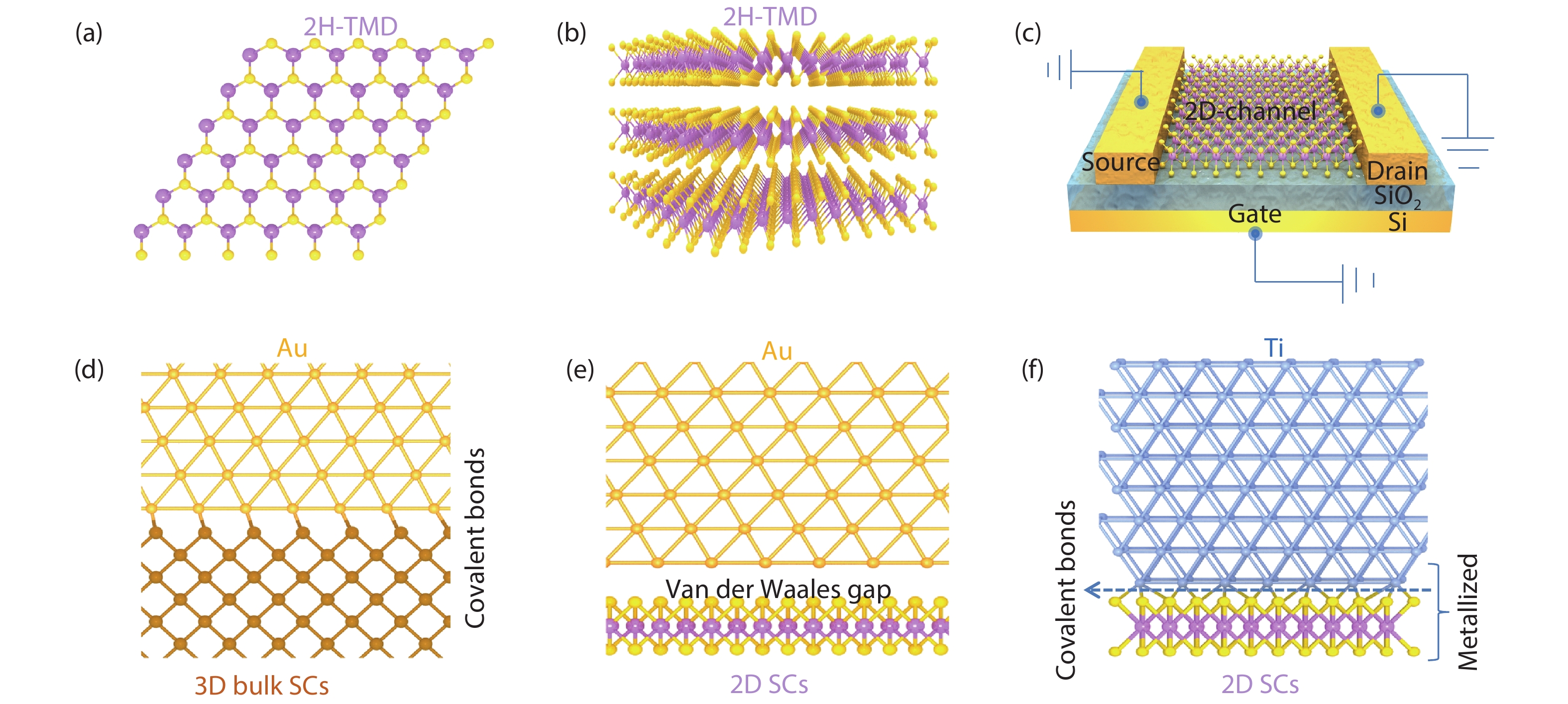
    Figure 1.(Color online) Atomic structure of representative 2D semiconductor materials and phase engineered contacts. (a, b) Top and side view of 2H stacked structure of 2D semiconductor. (c) Device model of 2D SCs based device. (d–f) Different types of metal–semiconductor junction with contact interface.

    3. Contact geometry and Schottky barrier of a metal-2D SC contact

    3.1. Contact geometry

    The field effect transistor (FET) is the most fundamental and common unit for electronic devices used in fundamental research and industry, as shown in Fig. 1(c). Heavily doped Si is used as the conductive substrate, where the back gated voltage is applied. The thermally oxidized SiO2 on Si substrate with thickness in the range of 90–300 nm is a dielectric layer and the 2D SCs can either be mechanically exfoliated or CVD grown onto the substrate. As the 3D top contact, the surface of bulk (3D) SCs tends to form covalent bonds with metals, shown in Fig. 1(d). However, for the metal-2D SC contact, it is difficult to form covalent bonds on the surface of 2D SCs. There will be a van der Waals gap between the interface of the metal (such as Au) and 2D SCs[57], as shown in Fig. 1(e). Allain et al. pointed out that this 3D top contact with van der Waals gap interface is an additional ‘tunnel barrier’ for carrier injection before the inherent Schottky barrier (SB)[58], which will result in a higher contact resistance. However, although an additional resistance may be caused by the non-bonding vdW gap, its Schottky tunnel barrier width (λSB) is too small (0.1 to 0.15 nm) to affect the carrier transport and can largely be neglected[59, 60]. In fact, owing to the existence of vdW gap, a cleaner metal-2D SCs interface can be formed and the crystal lattice of 2D SCs underneath the contact will be maintained in an unperturbed state, yielding to lower contact resistance and higher carrier mobility[61]. Another alternative method is to select a matched contact metal, which will be hybridized with the atoms of 2D SCs through covalent bonding. According to the density functional theory (DFT) calculation, covalent bonds can be formed at the interface between the 2D SCs and some specific metals, such as Ni for graphene[62], Ti for MoS2[63]. In the case of monolayer MoS2, the nonlocalized overlap states will be introduced in the bandgap of MoS2 by Ti contact, causing a totally metallized state of monolayer MoS2[57], as shown in Fig. 1(f). At this situation, the contact resistance decreases significantly. It should be noted that covalent bonding at the interface of metal-2D SCs may be out of work for multilayer 2D SCs because only the top layer can be hybridized, which will increase the contact resistance. Furthermore, Fermi level pinning effect has to be taken into account if the metal was hybridized with 2D SCs through covalent bonding[63] because the Schottky barrier height (ФSB) can be changed significantly by such effects.

    Although 3D top contact is commonly used between metal electrode and 2D SCs (Fig. 2(a)), considering the disadvantages of such contact, a 3D edge contact is proposed to overcome the Fermi level pinning effect at the interface (Fig. 2(b)). Both experiments and DFT calculation have shown the numerous advantageous of 3D edge contacts[64]. However, it is difficult to form a pure 3D edge contact by standard electron-beam lithography technique because of the atomically thin nature of 2D materials, where encapsulation of the SCs by hBN or thin oxide is needed[6569]. Apart from traditional metal contact, contacting 2D SCs using other 2D metallic materials is an elegant and convenient approach to decrease contact resistance and Schottky barrier. Schematic diagrams of 2D top contact and 2D edge contact are shown in Figs. 2(c) and 2(d), respectively. Three fundamental methods—CVD growth, phase engineering and intercalation treatment—are adopted to achieve 2D metallic contacts. High quality vertical and lateral heterostructures, such as VS2-MoS2, have been synthesized by the two step CVD method[7075]. These authors found that when compared to Ni/Au contact, the carrier mobility was improved at least four times and the ФSB was reduced from 163 to 30 meV by 2D metallic VS2 contact[75]. Similarly, heteroepitaxial stacking of monolayer metallic 1T-WTe2 and SC 2H-WSe2 was achieved by two step CVD growth[76]. A distinctively low contact barrier below 100 meV was established across a clean epitaxial vdW gap. Furthermore, other 2D metallic-SCs heterostructures, such as vertical NbTe2-WSe2 and lateral graphene–MoS2 heterostructures, are synthesized by two step CVD method, where the performance of the FETs is improved greatly by 2D metallic materials contact[77]. It is also possible to achieve a metallic state via direct substitutional doping, such as Nb doping induced metallic state in monolayer WS2, which can serve as a metallic contact[78, 79]. Aside from the CVD growth method, phase engineering is an effective way to transform the 2D SC into a metallic phase. By treating 2D SCs (e.g., monolayer or few layer MoS2) with n-butyl lithium, an uncovered region could be converted from 2H SC to 1T metallic phase[80]. In addition, Ar plasma or laser induced 2H SC to 1T metallic phase transition has also been reported by Zhu et al. and Cho et al.[80, 81]. The phase transition area of 2H–1T can be selected by the patterning process and the performance of these devices is substantially improved. Intercalation is also a promising method to turn the 2D SC to metallic state, which has seldom been explored to integrate 2D materials[82]. Combining with lithography, a spatially and size controlled metallic state could be realized by Co intercalation SnS2.

    (Color online) (a, b) 3D top contact and 3D edge contact configuration of metal-2D SCs contact. (c, d) 2D top contact and 2D edge contact of metallic 2D-SCs contact geometries.

    Figure 2.(Color online) (a, b) 3D top contact and 3D edge contact configuration of metal-2D SCs contact. (c, d) 2D top contact and 2D edge contact of metallic 2D-SCs contact geometries.

    3.2. Schottky barrier of a metal-2D SC contact

    In traditional Si-based CMOS integrated circuits, ohmic contacts are realized by heavy ion diffusion or implantation in body Si substrate. A simplified schematic diagram of an n-type MOS (NMOS) FET is shown in Fig. 3. The NMOS FET is fabricated on the p-type Si substrate, where the thickness of body Si is less than 1 mm generally. The Leff and tox are the effective channel length and thickness of oxide, and the typical value of which are about 0.15 μm and 50 Å, respectively[1, 2]. The driving force of the development of CMOS integrated circuits is to scale down the Leff and tox continuously. Source (S) and drain (D) are formed by heavy electron doping, also known as the n+ region. Heavily doped polycrystalline silicon is regarded as a gate electrode. The contact between the metal and the heavily doped region (source and drain) is called an ohmic contact. For conventional CMOS circuitry, an ohmic contact is essential to achieve high performance devices for either n or p type transports. The main indicator of an ohmic contact is the specific contact resistance (Rc), which can be defined by[1, 2]

    (Color online) Schematic diagram of a conventional Si-based NMOS FET.

    Figure 3.(Color online) Schematic diagram of a conventional Si-based NMOS FET.

    $ {R_{\rm{c}}\equiv \left(\frac{\partial J}{\partial V}\right)}_{V=0}^{-1}\quad ({\text{Ω}}\cdot{\rm{cm}}^{2}), $ (1)

    where J and V is current density and external bias voltage, respectively. For metal-SCs contact with low doping concentration of SCs, the thermionic emission current dominates. The characteristic of JV can be represented as[1, 2]

    $ J = {J_{\rm{s}}}\left[ {\exp\left( {\frac{{qV}}{{kT}}} \right) - 1} \right], $  (2)

    $ {J_{\rm{s}}} = {A^*}{T^2}{\rm{exp}}\left( {\frac{{ - q{\Phi _{{\rm{Bn}}}}}}{{kT}}} \right), $  (3)

    where Js, A*, T, k and is saturation current density, effective Richardson constant, absolute temperature, Boltzmann constant and barrier height, respectively. Combining the Eq. (1), Rc can be derived by[1, 2]

    $ {R_{\rm{c}}} = \frac{k}{{qT{A^*}}}\;{\rm{exp}}\left( {\frac{{q{\Phi _{\rm{Bn}}}}}{{kT}}} \right). $  (4)

    From Eq. (4), it can be found that Rc is proportion to , a smaller Rc will be achieved if using lower of metal-SCs contact. In contrast, if metal is contacted with heavily doped SCs, then the barrier width will be extremely narrow. In this situation, the tunneling current is dominant and can be estimated as[1, 2]

    $ I \sim \exp\left[ { - \frac{{{C_2}\left( {{\Phi _{{\rm{Bn}}}} - V} \right)}}{{\sqrt {{N_{\rm{D}}}} }}} \right], $  (5)

    $ {C_2} = {\rm{ }}4\sqrt {{m_{\rm{n}}}{\varepsilon _{\rm{s}}}}/\hbar, $  (6)

    where ND, mn, and ћ is concentration of donor, effective mass, dielectric constant of silicon and reduced Plank constant, respectively. Rc can be expressed by[1, 2]

    $ {R_{\rm{c}}} \approx {\rm{exp}}\frac{{{C_2}{\Phi _{{\rm{Bn}}}}}}{{\sqrt {{N_{\rm{D}}}} }} = {\rm{exp}}\;\frac{{4{\Phi _{{\rm{Bn}}}}\sqrt {{m_{\rm{n}}}{\varepsilon _{\rm{s}}}} }}{{\sqrt {{N_{\rm{D}}}} }}. $  (7)

    From Eq. (7), a small Rc can be realized by high doping concentration. As aforementioned, in conventional Si-based CMOS circuits, ohmic contacts are realized by heavy doping. However, when Si is substituted by 2D SCs, such controllable and sustainable doping strategies are not applicable to the 2D SCs based FET because of their fragility. Most contacts between metal and 2D SCs are Schottky contacts, which will increase contact resistance and limit the carrier injection. Therefore, reducing the ФSB of metal and 2D SCs contact is an effective way to improve carrier injection efficiency.

    Fig. 4(a) shows a schematic diagram of several metal-MoS2 band alignments along with work function of metal (ФM)[46, 49, 57, 63, 64]. The electron affinity (χ) of MoS2 can be given by the energy difference of conduction band Ec and the vacuum level Evac. Schottky barrier height, which is a tunnel barrier for carrier injection to cross the junction, is one of the most important parameters for the metal/SCs contact because it can fundamentally determine charge transport efficiency and impact device performance. If low ФM metal is aligned with the Fermi level (EF) close to the conduction band, then electron injection will be facilitated. Otherwise, if high ФM metal aligned with EF close to valence band, then hole injection will be promoted. In an ideal metal-2D SCs interface, ФSB is characterized by the Schottky–Mott rule, which is governed by electrostatics that involve energy-level alignments[83, 84].

    (Color online) (a) Schematic diagram of various metal–MoS2 band alignments along with work function of metal (ФM). The Fermi level of metal is lined up close to conduction band of MoS2. The left-hand part in Fig. 4(a) is the actual ФSB extracted from experiment, which is different from the theoretical value calculated by the difference of ФM (right-hand part in Fig. 4(a)) and electron affinity (χ) of MoS2. For example, theoretical values of ФSB for Sc–MoS2 and Pt–MoS2 contact are about –0.7 and 1.4 eV, respectively. However, the actual ФSB obtained from experiment is only 30 and 230 meV, indicating that there is a strong Fermi level pinning effect at the interface of metal and 2D SCs. (b) Energy band diagrams of MoS2 with and without 2D metallic materials.

    Figure 4.(Color online) (a) Schematic diagram of various metal–MoS2 band alignments along with work function of metal (ФM). The Fermi level of metal is lined up close to conduction band of MoS2. The left-hand part in Fig. 4(a) is the actual ФSB extracted from experiment, which is different from the theoretical value calculated by the difference of ФM (right-hand part in Fig. 4(a)) and electron affinity (χ) of MoS2. For example, theoretical values of ФSB for Sc–MoS2 and Pt–MoS2 contact are about –0.7 and 1.4 eV, respectively. However, the actual ФSB obtained from experiment is only 30 and 230 meV, indicating that there is a strong Fermi level pinning effect at the interface of metal and 2D SCs. (b) Energy band diagrams of MoS2 with and without 2D metallic materials.

    $ {\Phi _{{\rm{SB-n}}}}{\rm{ = }}{\Phi _{\rm{M}}}-{{\chi}_{\rm{S}}}, $  (8)

    $ {\Phi _{{\rm{SB-p}}}} = {E_{\rm{g}}} +{{\chi}_{\rm{S}}}-{\Phi _{\rm{M}}}, $  (9)

    where ФSB-n and ФSB-p are Schottky barrier heights for electrons and holes, respectively. Eg are bandgaps of the 2D SCs. Ideally, all of the parameters are followed by a Schottky–Mott rule and ФSB is linearly dependent on the ФM with a slope of unity. However, in fact, an ideal metal–2D SCs contact rarely forms and the ФSB is often incorrect estimated by Schottky–Mott mode, which was first noted by Bardeen in 1947[85]. According to the Bardeen limit, ФSB is usually independent on ФM, which lies between the Schottky and Bardeen limit. The Fermi level of metal is pinned to a nearly fixed position within the bandgap of SCs. For a given SC, the actual ФSB is given by Eq. (10) and the strength of Fermi-level pinning can be characterized by the interface S parameter (Eq. (11))[83]:

    $ {{{\Phi }}_{{\rm{SB-n}}}}=(S{{{\Phi }}_{\rm{M}}}-{{\chi }_{\rm{S}}})+(1-S){{{\Phi }}_{{\rm{IS}}}}, $  (10)

    $ S = {\rm{d}}{\Phi _{{\rm{SB-n}}}}{\rm{/d}}{\Phi _{\rm{M}}}, $  (11)

    where ФIS and S are the interface state energy of SC and Schottky pinning factor, respectively. If S = 0, then ФSB is independent of metal ФM, which indicates the strong pinning effect at the metal–SC interface. If S = 1, then ФSB is determined by Eqs. (1) and (2), and the Schottky–Mott limit is achieved. In the case of MoS2 and Ti contact, the theoretical value of ФSB is about 0.1 eV according to Eq. (8). The actual ФSB from experiment is about 50 meV[86], which is lower than that from the theoretical calculation. As shown in the left-hand part of the band alignments of various metal–MoS2 in Fig. 4(a), the Fermi level of metals (e.g., Sc, Ti, Ag and Pt etc.) locates in the bandgap of MoS2 near the conduction band[86]. It is worth mentioning that the extracted ФSB of 2D metallic VS2 contacted MoS2 device is only 30 meV, which is much lower than that from Ni–MoS2 contact (170 meV)[75]. As the interlayer between the metal and MoS2, the surface of the MoS2 was protected by VS2 and the Fermi level pinning effect can be avoided. The energy band diagrams of MoS2 without and with 2D metallic materials are shown in Fig. 4(b), where the ФSB was reduced in 2D metallic-SCs contact. The origin of the Fermi level pinning may be attributed to the charge redistribution at the interface of metal–2D SCs contact or the interaction between the contact metal and the chalcogen component[49, 57]. There is at present no consensus of the origin of Fermi level pinning and the origin has been discussed elsewhere[49, 57].

    4. Conventional metal contacts and 2D metallic material contacts

    In this part, we first discuss the strategies of conventional metal contacts (3D top contact and 3D edge contact) to decrease the contact resistance and improve carrier injection efficiency, including selecting matched contact metal, designing contact geometry, introducing special metal interlayer and metal transfer approaches. Next, strategies to introduce 2D metallic materials contacts (2D top contact and 2D edge contact) are discussed in detail, such as CVD growth of 2D metallic materials as contact, phase engineering of 2D SCs to metallic phase as contact. Finally, we discuss an intercalation strategy to induce metallic state.

    4.1. Conventional metal contacts

    4.1.1. Select matched contact metal

    Due to the lack of controllable and sustainable doping strategies for 2D SCs FET, the contact quality and resistance are determined by the contact metal. Therefore, a proper understanding and choice of source/drain contacts metals is essential to improve the performance of 2D SCs-based FETs. Das et al. presented a thorough experimental study of contacts to MoS2 by using different ФM metals such as Sc (ФM = 3.5 eV), Ti (ФM = 4.3 eV), Ni (ФM = 5.3 eV) and Pt (ФM = 5.6 eV)[86]. Figs. 5(a) and 5(b) show the prototype back gated MoS2 transistor and the corresponding SEM image. The AFM and optical images are shown in Fig. 5(c) and the inset figure, where the thickness of mechanical exfoliated MoS2 flake is about 3 nm. Assuming that an ideal interface has been formed by MoS2–metal, the ФSB will be determined by Schottky–Mott rule. The expected Fermi level of metal with the electronic bands of MoS2 is shown in Fig. 5(d), where only the difference of the electron affinity of MoS2 and the ФM of the corresponding metal is considered. The electron injection to conduction band should occur for low ФM metal of Sc and Ti, while high ФM metal Ni and Pt provide access to hole injection to valence band. In other words, n-type FET characteristics should be obtained by Sc and Ti contact, while p-type FET transfer curves can be observed. However, from the experimental transfer curves (Fig. 5(e)) it can be seen that all of the metal contacts present n-type FET characteristics, indicating that the Fermi levels of all the metals are lined-up close to conduction band of MoS2. The actual Fermi level of metal with the electronic bands of MoS2 is shown in the inset of Fig. 5(e). In addition, the on-state current is decreased from Sc to Pt contact at positive Vgs, indicating different carrier injection efficiency for various contact metals.

    (Color online) Metal contact investigation of MoS2 device. (a) Schematic diagram of back gated MoS2 transistor. (b, c) SEM and AFM images of device with MoS2 thickness of 3 nm. (d) The expected position of the metal Fermi level across the band of MoS2, where the ФSB was decided by the Schottky–Mott rule. (e) Transfer characteristics of MoS2 device with different contact metal. The inset is the actual position of Fermi level of from experimental date. (f) Temperature-dependent transfer curves with Ni contact, where the contribution of thermionic emission and thermally assisted tunneling are marked. (g) Arrhenius-type plot from (a). (h) Extracted actual ФSB for Ni-contacted MoS2 device. (i) The relationship of ФSB with metal work function[86]. Copyright 2013, American Chemical Society.

    Figure 5.(Color online) Metal contact investigation of MoS2 device. (a) Schematic diagram of back gated MoS2 transistor. (b, c) SEM and AFM images of device with MoS2 thickness of 3 nm. (d) The expected position of the metal Fermi level across the band of MoS2, where the ФSB was decided by the Schottky–Mott rule. (e) Transfer characteristics of MoS2 device with different contact metal. The inset is the actual position of Fermi level of from experimental date. (f) Temperature-dependent transfer curves with Ni contact, where the contribution of thermionic emission and thermally assisted tunneling are marked. (g) Arrhenius-type plot from (a). (h) Extracted actual ФSB for Ni-contacted MoS2 device. (i) The relationship of ФSB with metal work function[86]. Copyright 2013, American Chemical Society.

    Fig. 5(f) shows the temperature-dependent transfer curves with Ni contact, which was used to create the Arrhenius plot in Fig. 5(g). The actual ФSB can be revealed by the Arrhenius plot if the flat band voltage VFB is identified, and the VFB has been marked in Fig. 5(g). Note that the contributions of thermionic emission and thermally assisted tunneling are identified at different Vgs in Fig. 5(d). Based on the conventional thermionic emission theory, the slope of the curves in high-temperature region is presented. The ФSB is extracted by equation[86]:

    $ {I_{{\rm{ds}}}} = A{T^2}\exp[\left( {q{\Phi _{{\rm{SB}}}}} \right)/\left( {{k_{\rm{B}}}T} \right)] \{1 - \exp\left[ \left( {q{V_{{\rm{ds}}}}} \right)/\left( {{k_{\rm{B}}}T} \right)\right] \}, $  (12)

    where Ids, A, kB, q, T and Vds are the current through the device, Richardson’s constant, Boltzmann constant, electronic charge, temperature and source to drain bias, respectively. From Fig. 5(h), the extracted ФSB of Ni-contacted MoS2 is 150 meV, much lower than that calculated from Schottky–Mott rule. Fig. 5(i) shows the extracted ФSB from different metals with MoS2 as a function of their corresponding ФM. The ФSB is 30, 50, 150, and 230 meV for Sc, Ti, Ni, and Pt, respectively. The slope extracted by dФSB/dФM (interface parameter S) is about 0.1, which indicates strong Fermi level pinning effects at the metal–MoS2 interface and the Fermi levels of metal are pinned close to the conduction band in the bandgap of MoS2. It also explains why all of the metal contacts present n-type characteristics, even when using the large ФM metal. The carrier mobility of MoS2 with thickness of 10 nm is 184, 125, 36, and 21 cm2/(V·s) for Sc, Ti, Ni and Pt contact. However, the mobility is less than 20 cm2/(V·s) for Sc contact when the thickness of MoS2 is reduced to 3 nm. The results indicate that the performance of monolayer or few layer MoS2 FET can be further improved more effectively, except for the selection of the matched contact metal.

    4.1.2. Introducing a special interlayer metal

    Although the performance of 2D SCs FET can be improved by proper contact metal, the Fermi level pinning effect at the interface still limits the development of 2D SCs FETs. Creating van-der-Waals-type bonding between three-dimensional metal and 2D SCs is an ingenious method to improve the performance of 2D SCs FET. In a van-der-Waals-type contact, the contact resistance and ФSB can be decreased substantially. Furthermore, the Fermi level pinning effect at the metal–2D SCs interface can effectively be avoided[87]. Recently, Wang reported the realization of ultraclean van der Waals contacts between metal indium (In) and monolayer MoS2, where the 10 nm In capped by 100 nm protection layer of Au was deposited by standard laboratory electron-beam evaporator under normal vacuum (< 10−6 Torr)[87]. The contact resistance of In/Au electrodes is only about 3000 and 800 Ω·μm for monolayer and few layer MoS2, which is the lowest value obtained among metal electrodes evaporated onto MoS2. In addition, the carrier mobility reaches about 167 cm2/(V·s) for monolayer MoS2 based back-gated FET.

    Fig. 6(a) shows a schematic of the In/Au contacted MoS2 FET device. Cross-sectional annular dark field (ADF) scanning transmission electron microscopy (STEM) was used to verify the interface between In/Au–MoS2. Fig. 6(b) shows ADF and bright-field STEM images. The atomic resolution cross-sectional image of In/Au and MoS2 indicates that monolayer MoS2 is atomically sharp with no detectable evidence of reaction with In/Au. In addition, there is no observed damage on MoS2, indicating that In is gently deposited on the surface of MoS2. These results demonstrate the presence of a high-quality contact interface through the formation of van-der-Waals-type bonding of MoS2 and In layer. To investigate the performance of In/Au contacted MoS2 FET, contact resistance and FET properties are measured. Figs. 6(c) and 6(d) show the measured contact resistance of CVD growth monolayer (0.7 nm) and mechanically exfoliated few-layer (8 nm) MoS2 FETs using transmission line method (TLM). The contact resistance is 3.3 ± 0.3 kΩ·μm (at n = 5.0 × 1012 cm−2) and 800 ± 200 Ω·μm (at n = 3.1 × 1012 cm−2), respectively. Figs. 6(e) and 6(f) compare the contact resistance from the literature, indicating that the contact resistances achieved in this work are the lowest among all carrier concentrations. Figs. 6(g) and 6(h) present the room temperature and temperature-dependent transfer characteristics of monolayer and few-layer MoS2 FETs, respectively. A mobility of about 170 cm2/(V·s) can be achieved by using In/Au electrodes with monolayer MoS2 FET. Fig. 6(i) shows the output curves of monolayer MoS2 FET, where the linear output characteristics indicate the absence of a contact barrier and ohmic contact. The ФSB extracted from few-layer MoS2 in Fig. 6(j) is about 110 meV, which is consistent with the difference between work function of the metal and the conduction-band energy level of MoS2. Furthermore, the achieved ideal contact demonstrates that the Fermi level pinning effect is absent at this interface. In conclusion, this work provides a simple method to make ultraclean van der Waals contacts with standard industrial technology.

    (Color online) In contacted MoS2 transistors. (a) Device mode of MoS2 based back-gated device. The electrodes consist of 10 nm In layer capped with 100 nm Au. (b) Cross-sectional annular dark field (ADF) scanning transmission electron microscopy (STEM) of interface of In-MoS2. (c, d) Extracted contact resistance using transmission line method for MoS2 with thickness of 0.7 and 8.1 nm, respectively. (e, f) Comparison of contact resistance versus carrier concentration with different contact materials from literatures. (g, h) Transfer characteristics of device with monolayer MoS2 and temperature-dependent transfer curves for 8 nm MoS2 device. (i) Output curves with linear relationship indicates ohmic contact. (j) Extracted ФSB with value of 110 meV, indicates the ideal contact between the interface of In and MoS2, which is nearly the same as the value decided by the Schottky–Mott rule. The inset is the energy band diagram of MoS2 and In[87]. Copyright 2019, Nature Publishing Group.

    Figure 6.(Color online) In contacted MoS2 transistors. (a) Device mode of MoS2 based back-gated device. The electrodes consist of 10 nm In layer capped with 100 nm Au. (b) Cross-sectional annular dark field (ADF) scanning transmission electron microscopy (STEM) of interface of In-MoS2. (c, d) Extracted contact resistance using transmission line method for MoS2 with thickness of 0.7 and 8.1 nm, respectively. (e, f) Comparison of contact resistance versus carrier concentration with different contact materials from literatures. (g, h) Transfer characteristics of device with monolayer MoS2 and temperature-dependent transfer curves for 8 nm MoS2 device. (i) Output curves with linear relationship indicates ohmic contact. (j) Extracted ФSB with value of 110 meV, indicates the ideal contact between the interface of In and MoS2, which is nearly the same as the value decided by the Schottky–Mott rule. The inset is the energy band diagram of MoS2 and In[87]. Copyright 2019, Nature Publishing Group.

    4.1.3. Transfer metal electrode

    Another approach to improve the performance of 2D SCs FET is to transfer the electrode to the surface of 2D SCs, which has recently been reported by Duan et al.[60]. Similar to the results of In/Au contacted MoS2, a van der Waals contact without chemical disorder and Fermi level pinning between metal and MoS2 can be created by transferring metal films (silver or platinum) on MoS2. Ag or Pt contacted MoS2 two-terminal FETs can achieve an electron and hole mobility of 260 and 175 cm2/(V·s) at room temperature. Figs. 7(a)7(c) show the cross-sectional atomic structure and optical image of transferred Au electrode on top of MoS2. After peeling off the transferred metal electrode, the surface of MoS2 retains its original shape. This indicates that the MoS2 was not damaged during physical integration and the interface of metal-MoS2 does not form a direct chemical bonding. A cross-sectional TEM image of transferred Au contacted MoS2 is shown in Fig. 7(g), where the atomically sharp and clean metal-semiconductor interfaces can be observed. However, the surface of MoS2 was damaged by electron-beam-deposited Au electrode, as shown in Figs. 7(d), 7(f), and 7(h), which suggests direct chemical bonding and strong metal–semiconductor interaction in deposition process.

    (Color online) Transferred metal electrode contacted MoS2 FET. (a–c) Cross-sectional atomic mode and optical images of MoS2 device with transferred Au and the transferred Au mechanically released. (d–f) Cross-sectional schematics and optical images of MoS2 device with traditional electron-beam-deposited Au and the deposited Au mechanically released. (g, h) Cross-sectional schematics and TEM images of transferred and evaporated Au. (i, j) Transfer curves of MoS2 devices with different transferred and deposited metals. (k) Experimentally extracted ФSB for different transferred and evaporated metals[60]. Copyright 2018, Nature Publishing Group.

    Figure 7.(Color online) Transferred metal electrode contacted MoS2 FET. (a–c) Cross-sectional atomic mode and optical images of MoS2 device with transferred Au and the transferred Au mechanically released. (d–f) Cross-sectional schematics and optical images of MoS2 device with traditional electron-beam-deposited Au and the deposited Au mechanically released. (g, h) Cross-sectional schematics and TEM images of transferred and evaporated Au. (i, j) Transfer curves of MoS2 devices with different transferred and deposited metals. (k) Experimentally extracted ФSB for different transferred and evaporated metals[60]. Copyright 2018, Nature Publishing Group.

    Fig. 7(i) shows the transfer characteristics of MoS2 with electron-beam-deposited metal electrode. All of the devices present n-type behavior irrespective of metals with high or low ФM, which is consistent with previous studies[21, 49]. This can be assigned to the strong Fermi level pining near the conduction band of MoS2. In contrast, for transferred metal electrodes, the carrier type can be tailored from electrons to holes by changing the ФM of contact metal, as shown in Fig. 7(j). The ФSB extracted from experiment as function of ФM for different transferred and evaporated metals are presented in Fig. 7(k). For transfer electrode contacted MoS2 FET, the ФSB is strongly dependent on the metal ФM with a slope of 0.96 (S = 0.96), approaching thee Schottky–Mott limit. In contrast, the slope is only 0.09 (S = 0.09) for transitional electron-beam-deposited metal contact, which indicates the strong pinning effect at the metal–MoS2 interface. The electron mobility of Ag transfer contacted MoS2 FET is 260 cm2/(V·s) while the hole mobility of Pt transfer contacted is 175 cm2/(V·s). This work provides a general, low-energy metal integration approach to achieve high performance of 2D FET.

    4.1.4. Metal edge contact

    Considering the aforementioned limits of a 3D top contact, 3D edge contact has proven to be highly advantageous when compared with a 3D top contact in terms of carrier injection efficiency[86-90]. A 3D top contact has a wide tunnel barrier for its unfavorable out-of-plane carrier transport interface with low degree of covalency, while 3D edge contact has a more favorable in-plane carrier transport interface and smaller tunnel barrier. Though 3D edge contact has many benefits, it is difficult to realize pure edge contact by standard lithographic techniques. Recently, Wang et al. achieved the pure edge contact by capping insulting layer h-BN on the surface of graphene before metal deposition[65]. The insulating capping layer prevents the top surface of graphene from the direct contact with metal. The obtained contact resistance is as low as 100 Ω·μm and room temperature mobility reaches the theoretical phonon scattering limit[65]. Similarly, based on this method, h-BN encapsulated MoS2 device with graphene edge contact was achieved by Cui et al., as shown in Fig. 8(a)[66]. This method uses graphene as the bridge between MoS2 and metal. Figs. 8(b)8(d) show the temperature-dependent output curves, contact resistance and temperature-dependent Hall mobility, respectively. The linear output curves in Fig. 8(b) indicate the ohmic contact of this device. The record-high Hall mobility of 34 000 cm2/(V·s) was achieved at low temperature, and 120 cm2/(V·s) at room temperature, indicating the high contact quality.

    (Color online) Edge contact investigation of MoS2 device. (a) Schematic diagram of hBN encapsulated MoS2 device with graphene edge contact. (b–d) Temperature dependent output curves, contact resistance and temperature dependent Hall mobility, respectively[66]. Copyright 2016, Nature Publishing Group (e) Schematic of Al2O3 capped edge contacted MoS2 device. (f–h) Output curves, transfer characteristic and mobility with different drain voltage for Al2O3 capped MoS2 device. (i) Schematic of h-BN capped edge contacted MoS2 device. (j–l) Output curves, transfer characteristic and mobility with different drain voltage for hBN capped MoS2 device[67]. Copyright 2016, WILEY-VCH Verlag GmbH & Co. KGaA, Weinheim.

    Figure 8.(Color online) Edge contact investigation of MoS2 device. (a) Schematic diagram of hBN encapsulated MoS2 device with graphene edge contact. (b–d) Temperature dependent output curves, contact resistance and temperature dependent Hall mobility, respectively[66]. Copyright 2016, Nature Publishing Group (e) Schematic of Al2O3 capped edge contacted MoS2 device. (f–h) Output curves, transfer characteristic and mobility with different drain voltage for Al2O3 capped MoS2 device. (i) Schematic of h-BN capped edge contacted MoS2 device. (j–l) Output curves, transfer characteristic and mobility with different drain voltage for hBN capped MoS2 device[67]. Copyright 2016, WILEY-VCH Verlag GmbH & Co. KGaA, Weinheim.

    Note that the edge contact in Fig. 8(a) is bridged by graphene and is not directly edge contacted with 2D SCs. Chai et al. fabricated the pure edge contacted MoS2 device through pre-deposition Al2O3 by ALD or encapsulated h-BN on MoS2[67]. Figs. 8(e) and 8(i) show the schematic illustration of preparation process called “passivation first, metallization second technique”. Figs. 8(f)8(h) show the electrical properties of the Al2O3 capped edge-contacted MoS2 device, where the Schottky contact is obtained and the maximum mobility is about 9 cm2/(V·s). Figs. 8(j)8(l) show output curves and transfer characteristic of the h-BN capped MoS2 device. Its calculated contact resistance is about 314 kΩ and the mobility is only 1.2 cm2/(V·s) for the h-BN encapsulated device, which indicate that it may not be a truly ohmic contact even if the apparent linear dependence of current on drain voltage, as Das demonstrated in their report[86]. The results indicate that the edge contact quality between metal and MoS2 using this “passivation first, metallization second technique” should be optimized in future.

    4.2. Metallic 2D material contacts

    Apart from conventional metal contact, integrating 2D metallic materials on SCs to form van der Waals contact is also an attractive way to eliminate Fermi level pinning effect and decrease the contact resistance. Furthermore, 2D metallic-SCs heterostructures have wide potential in future applications, such as high-performance transistors[25, 28], phototransistors[32, 38] and so on. In this part, we will discuss CVD growth of 2D metallic materials as contact, phase engineering of 2D SCs to metallic phase as contact, and intercalation method to induce 2D SCs into metallic state as contact. For the 2D top contact, the 2D metallic materials can be regarded as a protection and buffer layer. In the case of CVD growth 2D metallic materials as top contact, the out-of-plane van der Waals bonding will be formed between 2D SCs and metallic materials. The surface of 2D SCs will not be damaged by the deposited metal. A van der Waals type contact will facilitate the carrier injection across the interface, which was also demonstrated by In/Au contacted 2D SCs, as we discussed previously in Section 4.1.2. In addition, Fermi level pinning effect can be avoided and then the contact resistance can be reduced by such contact. However, compared to the 2D edge contact with metallic materials grown by CVD, there is a larger tunnel barrier in 2D top contact because of the van der Waals contact mode. Higher carrier injection efficiency can be achieved by in-plane covalent bonding between 2D SCs and metallic materials owing to the smaller tunnel barrier widths in a 2D edge contact.

    Besides CVD growth method, phase engineering and intercalation can also introduce 2D metal–SCs in-plane heterostructure. The metallic state can be realized by point defects through laser or Ar plasma treatment, or introducing interlayer metal atoms through intercalation approaches, which is similar to the heavy doping technology in Si-based CMOS circuits. Therefore, this type of 2D SCs FET can be regarded as a simplified conventional Si-based NMOS FET. The difference is that doping technology in Si-based CMOS circuits is controllable and sustainable, while doping strategies for 2D SCs FET can only be applied to certain 2D SCs.

    4.2.1. CVD growth 2D metallic materials as contact

    The CVD method can produce many kinds of 2D metallic-SCs heterostructures with high yield, including the stacking orientation controlled vertical and seamless lateral 2D metallic-SCs heterostructures[71-75]. Therefore, CVD is regarded as one of the most promising methods to build 2D integrated circuits for future applications. To take one example, uses CVD growth 2D metallic materials as contact to decrease the contact resistance and enhance the performance of 2D SCs FET.

    Recently, Lee et al. and Duan et al. achieved heteroepitaxial stacking of van der Waals monolayer 1T metallic-2H SC WSe2 heterostructures, in which a distinctively low contact barrier was achieved across a clean epitaxial van der Waals gap[76, 77]. Fig. 9(a) shows a schematic illustration of a two-step CVD method growing metallic WTe2-SC WSe2 heterostructure, where the monolayer WSe2 was synthesized first followed by the growth of metallic WTe2. Fig. 9(b) shows the illustration of device schemes of WTe2 (FET-1) and Ti/Au (FET-2) contact. The output current of WTe2 contact WSe2 FET is much larger than its counterpart from Ti/Au contact (Fig. 9(c)), which indicates high carrier injection efficiency with WTe2 contact. The temperature-dependent sheet conductivity (σ) versus bake gate voltage (Vg) curves are shown in Fig. 9(d). The current on–off ratio of WTe2 contact device is about 107, which is larger than that from Ti/Au contact WSe2 FET (~ 105). In addition, the maximal hole mobility is about 20 cm2/(V·s) for WTe2 contact device, which is at least ten times higher than that of Ti/Au contact. Using thermionic emission model, ФSB height extracted from Fig. 9(e) for WTe2 contact device is about 70 meV while the ФSB height is about 126 meV from Ti/Au contact. The reduced ФSB demonstrates that the Fermi level pinning effect can be eliminated by the 2D metallic contact. The parameters of interface S is about 0.065 and 1 from the curves slope in Fig. 9(f). The performance of WSe2 FET also can be improved by 1T metallic NbTe2 contact, where the atomic structure, optical image of heterostructure and device models are shown in Figs. 9(g)9(j). The on-state current is 2.68 μA/μm at Vds = 1.5 V for NbTe2 contacted WSe2 FET, which is twice over the one in Cr/Au contact device (Figs. 9(k) and 9(m)). Correspondingly, the hole mobility of NbTe2 contact device is at least two times higher than that for Cr/Au contact, as seen in Figs. 9(l) and 9(n). The performance improvement can be attributed to the unbroken surface of the WSe2, where the Fermi level pinning effect at the interface is avoided.

    (Color online) Contact engineering of vertical 2D metallic-2H WSe2 heterostructure. (a) Sequential growth scheme of vertical WSe2 and WT2 heterostructure. The inset is the optical images of WSe2 and WTe2. (b) Device mode of WSe2 with and without contact. (c, d) Output curves and temperature-dependent conductivity of WSe2 device with WTe2 and Ti contact. (e) Built-in potential energy versus back-gated voltage for Ti and WTe2 contacted WSe2 devices. (f) ФSB height with the function of metal work function[76]. Copyright 2013, American Chemical Society. (g, h) Atomic structure of van der Waals epitaxy growth of 2D metallic-SCs heterostructure and optical image of NbTe2-WSe2 heterostructure. (i, j) Schematic model of WSe2 device with NbTe2 and Ti contact. (k–n) Current–voltage and transfer characteristics of WSe2 device with and without NbTe2 contact. The inset is optical images of fabricated devices[77]. Copyright 2019, WILEY-VCH Verlag GmbH & Co. KGaA, Weinheim.

    Figure 9.(Color online) Contact engineering of vertical 2D metallic-2H WSe2 heterostructure. (a) Sequential growth scheme of vertical WSe2 and WT2 heterostructure. The inset is the optical images of WSe2 and WTe2. (b) Device mode of WSe2 with and without contact. (c, d) Output curves and temperature-dependent conductivity of WSe2 device with WTe2 and Ti contact. (e) Built-in potential energy versus back-gated voltage for Ti and WTe2 contacted WSe2 devices. (f) ФSB height with the function of metal work function[76]. Copyright 2013, American Chemical Society. (g, h) Atomic structure of van der Waals epitaxy growth of 2D metallic-SCs heterostructure and optical image of NbTe2-WSe2 heterostructure. (i, j) Schematic model of WSe2 device with NbTe2 and Ti contact. (k–n) Current–voltage and transfer characteristics of WSe2 device with and without NbTe2 contact. The inset is optical images of fabricated devices[77]. Copyright 2019, WILEY-VCH Verlag GmbH & Co. KGaA, Weinheim.

    Lateral 2D metallic-SCs heterostructures are also utilized to fabricate device with 2D metallic material contact. Figs. 10(a) and 10(e) show a schematic model of lateral graphene–MoS2 heterostructures[91, 92]. A device model of lateral VS2–MoS2 heterostructures[75] is presented in Fig. 10(i). As the MoS2 FET contacted with metallic graphene or VS2, the mobility can be improved substantially when compared to the traditional metal contact. The electrical characterizations of graphene contacted MoS2 FET are shown in Figs. 10(b)10(d) and Figs. 10(f)10(h). As reported by Zhang et al., current on–off ratio of 107 and maximum field effect mobility of 24 cm2/(V·s) was obtained, which is much higher than its counterparts from Au contact. A similar improvement is also achieved by Hong et al. in graphene contacted MoS2 device, in which a high on–off ratio of about 109 and maximum field effect mobility of 8.5 cm2/(V·s) were presented. Figs. 10(j)10(l) show the output characteristics, ФSB and contact resistances with different back gate voltage, respectively. The output current from the VS2 contacted device is about six times higher than that from the Ni-contacted counterpart. As expected, the mobility was improved from 5.5 cm2/(V·s) for Ni/Au contact device to 35 cm2/(V·s) for VS2 contacted device. The enhanced mobilities of the device can be attributed to the reduced ФSB and contact resistance[93-96]. As shown in Figs. 10(k) and 10(l), the ФSB is as small as 30 meV, getting one of the lowest ФSB in the previous reports, which is far less than that from Ni/Au contact (ФSB = 163 meV). The contact resistance in VS2 contacted MoS2 device is 520 Ω·μm at Vg = 50 V, which is ten times smaller than that of Ni−MoS2 contacts (8640 Ω·μm).

    (Color online) Contact engineering of lateral graphene–MoS2 and VS2–MoS2 heterostructures. (a) Schematic diagram of MoS2–graphene lateral heterostructure. (b, c) Transfer and output curves of graphene contacted MoS2 device. (d) Statistics of obtained mobility from graphene contacted MoS2 device[91]. Copyright 2016, Nature Publishing Group. (e) Schematic fabrication of the MoS2–graphene lateral heterostructure. (f, g) Representative transfer and output curves of graphene contacted MoS2 deice. (h) Total, contact and channel resistance of graphene contacted MoS2 device[92]. Copyright 2016, WILEY-VCH Verlag GmbH & Co. KGaA, Weinheim. (i) Device schematic of VS 2 contacted MoS2. (j) Ids–Vds curves of MoS2 device with VS2 and Ni contact. (k) Extracted ФSB of VS2 and Ni contacted MoS2 as a function of Vbg. (l) Contact resistance of Ni and VS2 contacted MoS2 devices[75]. Copyright 2018, American Chemical Society.

    Figure 10.(Color online) Contact engineering of lateral graphene–MoS2 and VS2–MoS2 heterostructures. (a) Schematic diagram of MoS2–graphene lateral heterostructure. (b, c) Transfer and output curves of graphene contacted MoS2 device. (d) Statistics of obtained mobility from graphene contacted MoS2 device[91]. Copyright 2016, Nature Publishing Group. (e) Schematic fabrication of the MoS2–graphene lateral heterostructure. (f, g) Representative transfer and output curves of graphene contacted MoS2 deice. (h) Total, contact and channel resistance of graphene contacted MoS2 device[92]. Copyright 2016, WILEY-VCH Verlag GmbH & Co. KGaA, Weinheim. (i) Device schematic of VS 2 contacted MoS2. (j) IdsVds curves of MoS2 device with VS2 and Ni contact. (k) Extracted ФSB of VS2 and Ni contacted MoS2 as a function of Vbg. (l) Contact resistance of Ni and VS2 contacted MoS2 devices[75]. Copyright 2018, American Chemical Society.

    4.2.2. Phase engineering 2D semiconductor into metallic phase

    Compared to CVD grown 2D metallic-SCs heterostructures, the phase engineering method is more specific. On the one hand, it can only be applied to 2D SCs that have two or more stable or metastable phases; while on the other hand, the phase transition region can be patterned selectively. For example, the stable phase on MoS2 is trigonal prismatic (H) coordination and a semiconductor while the MoS2 with octahedral (T) coordination is a metastable phase with metallic nature[53, 96, 97]. The achieved metallic T phase can be worked as atomically seamless ohmic contact for 2D SCs device.

    Electron donation induced phase transition—such as n-butyl lithium treatment[80], chalcogen vacancies induced by laser irradiation[80] or by Ar plasma treatment[81]—is one of the most widely used phase engineering methods to transform 2D SCs into metallic state. During these processes, the exposed area can be converted to metallic 1T phase while the covered region remains 2H SC phase. Fig. 11(a) shows an electrostatic force microscopy phase image of monolayer MoS2 treated by n-butyl lithium, where the exposed regions are converted to 1T metallic phase while the protected regions remain 2H SC phase, forming a 1T–2H–1T lateral heterostructure. Figs. 11(b)11(d) present the device performance of 1T metallic MoS2 contacted 2H MoS2 device. Compared to Au contacted MoS2 device, the contact resistance reduced from 1.1 to 200 kΩ·μm and its ohmic contact was achieved by 1T MoS2 contacted. In addition, the mobility was improved from 19 to 46 cm2/(V·s) and the subthreshold swing values of 1T-MoS2 contacted FETs are much smaller than that of Au contacted. Similarly, through laser-irradiation, the mobility of 1T’ MoTe2 contacted 2H channel MoTe2 device was improved from about 1 to 50 cm2/(V·s) (Fig. 11(h)) and the ФSB was reduced from 200 to 10 meV compared to the counterpart of metal contacted 2H MoTe2 device. A schematic illustration and the transistor model are shown in Figs. 11(e) and 11(f). Furthermore, Ar plasma induced 2H–1T phase transition of MoS2 also reported by Zhu et al. A schematic diagram of plasma-treated process is shown in Fig. 11(i). The schematic modes of three types of devices are shown in Fig. 11(j) and the output and transfer characteristics of back gated monolayer MoS2 device are shown in Figs. 11(k) and 11(l). Although the contact is a mixture of 2H and 1T phase, the contact resistance can still be reduced, which was demonstrated by the increased output current in Fig. 11(k).

    (Color online) Electron donation, laser or Ar plasma induced metallic phase as contact. (a) Electrostatic force microscopy phase image of 1T–2H–1T lateral MoS2 heterostructure. (b–d) Resistance, output and transfer curves of 2H phase MoS2 with metallic 1T phase MoS2 contact. The inset is the device model of MoS2 device with Au and 1T metallic MoS2 contact[80]. Copyright 2014, Nature Publishing Group. Laser induced phase transition of metallic 1T’-MoTe2. (e) Atomic structure and laser treated process. (f) Device schematic with metallic 1T’-MoTe2 contact. (g) Output characteristic of MoTe2 device with 1T’-MoTe2 contact. (h) Field-effect mobility as a function of temperature of MoTe2 device with Au and metallic MoTe2 contact2 contact[80]. Copyright 2015, American Association for the Advancement of Science (AAAS). (i) Atomic structure and schematic representation of plasma-treated process. (j) Device models with Au or 1T/2H phase MoS2 contact. (k, l) Output and transfer curves with different Au and 1T/2H phase MoS2 contact[81]. Copyright 2017, American Chemical Society.

    Figure 11.(Color online) Electron donation, laser or Ar plasma induced metallic phase as contact. (a) Electrostatic force microscopy phase image of 1T–2H–1T lateral MoS2 heterostructure. (b–d) Resistance, output and transfer curves of 2H phase MoS2 with metallic 1T phase MoS2 contact. The inset is the device model of MoS2 device with Au and 1T metallic MoS2 contact[80]. Copyright 2014, Nature Publishing Group. Laser induced phase transition of metallic 1T’-MoTe2. (e) Atomic structure and laser treated process. (f) Device schematic with metallic 1T’-MoTe2 contact. (g) Output characteristic of MoTe2 device with 1T’-MoTe2 contact. (h) Field-effect mobility as a function of temperature of MoTe2 device with Au and metallic MoTe2 contact2 contact[80]. Copyright 2015, American Association for the Advancement of Science (AAAS). (i) Atomic structure and schematic representation of plasma-treated process. (j) Device models with Au or 1T/2H phase MoS2 contact. (k, l) Output and transfer curves with different Au and 1T/2H phase MoS2 contact[81]. Copyright 2017, American Chemical Society.

    4.2.3. Intercalation induced metallic state

    Intercalation is a convenient and promising method to tune the properties of van der Waals materials[82]. Figs. 12(a) and 12(b) show the schematics of the atomic structure of bilayer pristine SnS2 with a van der Waals gap and Co, Cu intercalated SnS2, respectively. The n-type SnS2 was converted to p-type semiconductor and a highly conductive metal by Cu and Co intercalation, respectively. Figs. 12(c)12(f) show optical images of CVD-grown SnS2, Cu–SnS2, Co–SnS2 and spatially controlled intercalation of SnS2, respectively, where the morphologies stay the same after intercalation while the colors of Cu–SnS2 and Co–SnS2 become more opaque and turn dark blue and violet-red. Temperature-dependent resistance measurement was performed to verify the electrical characteristic of intercalated SnS2 (Fig. 12(g)). One can see that the resistance of Co–SnS2 is almost independent of temperature and gives a metallic behavior, while Cu–SnS2 presents typical semiconducting behavior. Fig. 12(h) shows the typical transfer curve of Cu–SnS2 FET, showing the p-type behavior. To verify whether the performance of metallic Co–SnS2 contacted device can be improved, Co–SnS2 contacted SnS2, Cu–SnS2 and p–n junction FETs are fabricated. The output curves are shown in Figs. 12(i) and 12(j), respectively. It can be seen that the current of all of the Co–SnS2 contacted devices is improved compared to the Ti/Au contacted SnS2 FET, which indicates the good contact quality formed by metallic Co–SnS2.

    (Color online) Intercalation induced phase transition of SnS2. (a) and (b) Atomic structures of pristine SnS2, Cu and Co intercalated SnS2. (c–f) Optical images of pure SnS2, Cu, Co and Cu–Co intercalated SnS2. (g) Temperature-dependent resistance of SnS2, Cu–SnS2, Co–SnS2 and few layer graphene, where the Cu–SnS2 presents semiconductor behavior while the Co–SnS2 behaves as a metal like graphene. (h) Transfer curves of Cu–SnS2 with p-type characteristic. (i) I–V curves of Co–SnS2 contacted SnS2 and Cu–SnS2 devices. (j) SnS2/Cu–SnS2 junction with and without metallic Co–SnS2 contact[82]. Copyright 2018, Nature Publishing Group.

    Figure 12.(Color online) Intercalation induced phase transition of SnS2. (a) and (b) Atomic structures of pristine SnS2, Cu and Co intercalated SnS2. (c–f) Optical images of pure SnS2, Cu, Co and Cu–Co intercalated SnS2. (g) Temperature-dependent resistance of SnS2, Cu–SnS2, Co–SnS2 and few layer graphene, where the Cu–SnS2 presents semiconductor behavior while the Co–SnS2 behaves as a metal like graphene. (h) Transfer curves of Cu–SnS2 with p-type characteristic. (i) IV curves of Co–SnS2 contacted SnS2 and Cu–SnS2 devices. (j) SnS2/Cu–SnS2 junction with and without metallic Co–SnS2 contact[82]. Copyright 2018, Nature Publishing Group.

    5. Summary and outlook

    In summary, in this review we have discussed the fundamental aspects related to contacts of 2D materials devices, including contact geometry and Schottky barrier. We also presented the progress of contact engineering strategies to improve the contact quality. In the conventional metal contact part, we show that the performance of 2D SCs FET can be improved by the right choice of top contact metal. However, the Fermi level pinning effect at the interface cannot be avoided, resulting in Schottky contact between top metal and 2D SCs. Fortunately, an ohmic contact can be realized and the Fermi level pinning effect can be eliminated by van-der-Waals-type bonding or gap through introduction of an In interlayer or metal electrode transfer method. A 3D edge contact was also emphasized and developed because it is advantageous over 3D top contact in terms of carrier injection efficiency, even if the pure edge contact technology is in the initial stage. However, the fabrication process of these 3D top contact or edge contact method is still complicated and faces the difficulties of scalable production.

    Compared to traditional metal contact, a van-der-Waals-type metallic contact can easily be achieved by 2D metallic materials grown through CVD method. The performance of 2D SCs FET has improved substantially owing to the elimination of Fermi level pinning effect and reduction of ФSB and contact resistance. But the properties of 2D SCs may be degraded after the growth of 2D metallic materials because the defects and impurities may be introduced in 2D SC’s lattice and surface at high temperature. This disadvantage can be avoided by phase engineering or intercalation methods. The phase engineering method is an effective way to achieve ohmic contact for 2D SCs FET. The problem of this method is that the induced T phase is unstable and may return to the H phase as time goes on or at temperatures above 100 °C. In contrast, transition metal intercalation induced metallic state is very stable, which makes it a promising post-growth treatment method to fabricate spatially controlled atomically seamless in-plane 2D metallic-SCs heterostructure. The limitation of the intercalation method is that it cannot be applied to all the 2D materials and the interfaces of the resulted heterostructures have not been well characterized. If the intercalation method can be further developed and applied to those 2D SCs with strong interlayer van der Waals coupling, for example double layer MoS2 or WS2, then it will be a tremendous advance and will facilitate the application of this method to 2D SCs based transistors.

    Although great progress has been achieved in the field of contact engineering for 2D SCs, there are still some challenges to solve. First, the origin of Fermi level pinning effect is still in debate. Some possible mechanisms, such as charge redistribution induced interface dipoles at interface of metal and 2D SCs or contact metal and chalcogen interaction caused orbital overlap are believed to be responsible for the Fermi level pinning effect[97-100]. Accurate experiments should be developed to analyze the contact interface of metal and 2D SCs, which is important for our understanding of Fermi level pinning effect and Schottky barrier. Therefore, more efforts are needed to uncover and resolve this detrimental effect.

    Second, phase engineering or intercalation method induced 2H–1T in-plane heterostructure has previously been reported but, up to now, the barrier at 2H–1T boundary has not been systematically studied. It is necessary to propose a method to predict or calculate the boundary barrier, which will guide us to fabricate high quality heterostructure with ignored tunneling width for carrier injection across the boundary.

    Third, it is well known that 2D materials with excellent optical and electrical properties are promising alternatives of Si in future applications in CMOS integrated circuits, and the device dimensions can be further scaled down owing to the atomically thin nature. However, up to now, all the contact engineering strategies reported are limited to a few 2D materials. There are no universal and scalable strategies that can be applied to a highly scaled device in a manufactural way. Before the practical application of contact engineering strategies in modern circuits, wafer scale single crystal with thickness controlled 2D SCs must be made. CVD is one of the most promising methods to get wafer-scale 2D materials, but well crystallinity, repeatability and controllability are still hard to obtain. In addition, an accurate and suitable method should be exploited to precisely control the nucleation position of heterostructures. Very recently, Duan et al. provided a general scalable synthesis method to precisely control the nucleation position and growth process of 2D metallic-SCs heterostructures[101]. As shown in Figs. 13(a) and 13(b), periodic defect arrays have been patterned on 2D SCs (MoS2, WSe2 and WS2) by 488 nm laser, where the 2D metallic materials (VSe2, VS2, CoTe2, NiTe2 and NbTe2) are nucleated at such sites. Figs. 13(c)13(e) show the optical images of periodic arrays of 2D metallic-WSe2 heterostructures, where thick 2D metallic materials are grown on the pre-patterned sites periodically. An optical image and the electrical properties of 2D metallic VS2 contacted WSe2 FETs are shown in Figs. 13(f)13(g). It can be seen that the performance of a WSe2 FET is improved greatly by VSe2 contact, indicating the feasibility of this scalable method. Finally, other controllable and sustainable contact engineering strategies should be exploited, such as exploiting a general scalable synthesis method to grow atomically thin in-plane 2D metallic-SCs heterostructures, looking for a general phase engineering method, improving the universality of intercalation method or developing transplantable 2D metallic arrays to fabricate 2D metallic-SCs heterostrutures accurately. It should be emphasized that wafer scale single crystal with thickness controlled 2D SCs must be realized before practical application in modern integrated circuits. The application of 2D materials to modern integrated circuits is still in its infancy, therefore it is necessary to develop a reliable, reproducible, and robust method to get 2D integrated circuits in the future.

    (Color online) General scalable synthesis of precisely controlled nucleation position and growth process of 2D metallic-SCs heterostructures. (a) Schematic process of selectively patterned periodic defect arrays of 2D SCs (MoS2, WSe2 and WS2) to grow 2D metallic materials (VSe2, VS2, CoTe2, NiTe2 and NbTe2). (b) Schematic diagram of VSe2 growth on patterned sites of WSe2. (c–e) Optical images of periodical arrays of 2D metallic materials on WSe2. (f) Optical image of VSe2 contacted WSe2 FET periodical arrays. (g–j) Electrical characterizations of the VSe2 contacted WSe2 FET[101]. Copyright 2020, Nature Publishing Group.

    Figure 13.(Color online) General scalable synthesis of precisely controlled nucleation position and growth process of 2D metallic-SCs heterostructures. (a) Schematic process of selectively patterned periodic defect arrays of 2D SCs (MoS2, WSe2 and WS2) to grow 2D metallic materials (VSe2, VS2, CoTe2, NiTe2 and NbTe2). (b) Schematic diagram of VSe2 growth on patterned sites of WSe2. (c–e) Optical images of periodical arrays of 2D metallic materials on WSe2. (f) Optical image of VSe2 contacted WSe2 FET periodical arrays. (g–j) Electrical characterizations of the VSe2 contacted WSe2 FET[101]. Copyright 2020, Nature Publishing Group.

    Acknowledgements

    This work was supported by the National Key R&D Program of China (Grant No. 2018YFA0306900) and the Natural Science Foundation of China (Grant No. 51872012).

    References

    [1] R Schaller. Moore's law: past, present and future. IEEE Spectrum, 34, 52(1997).

    [2] D J Frank, R H Dennard, E Nowak et al. Device scaling limits of Si MOSFETs and their application dependencies. Proc IEEE, 89, 259(2001).

    [3] D Sarkar, X J Xie, W Liu et al. A subthermionic tunnel field-effect transistor with an atomically thin channel. Nature, 526, 91(2015).

    [4] A J Arnold, A Razavieh, J R Nas et al. Mimicking neurotransmitter release in chemical synapses via hysteresis engineering in MoS2 transistors. ACS Nano, 11, 3110(2017).

    [5] Y J Gong, G Shi, Z H Zhang et al. Direct chemical conversion of graphene to boronand nitrogen-and carbon-containing atomic layers. Nat Common, 5, 3193(2014).

    [6] Y L Xie, B Lian, B Jäck et al. Spectroscopic signatures of many-body correlations in magic-angle twisted bilayer graphene. Nature, 572, 101(2019).

    [7] L F Li, W Liu, A Y Gao et al. Plasmon excited ultrahot carriers and negative differential photoresponse in a vertical graphene van der Waals heterostructure. Nano Lett, 19, 3295(2019).

    [8] K S Novoselov, A K Geim, S V Morozov et al. Two-dimensional gas of massless Dirac fermions in graphene. Nature, 438, 197(2005).

    [9] Y B Zhang, Y W Tan, H L Stormer et al. Experimental observation of the quantum Hall effect and Berry's phase in graphene. Nature, 438, 201(2005).

    [10] C Lee, X D Wei, J W Kysar et al. Measurement of the elastic properties and intrinsic strength of monolayer graphene. Science, 321, 385(2008).

    [11] Y P Liu, I Yudhistira, M Yang et al. Phonon-mediated colossal magnetoresistance in graphene/black phosphorus heterostructures. Nano Lett, 18, 3377(2018).

    [12] S Y Huang, G W Zhang, F R Fan et al. Strain-tunable van der Waals interactions in few-layer black phosphorus. Nat Common, 10, 2447(2019).

    [13] K Chaudhary, M Tamagnone, M Rezaee et al. Engineering phonon polaritons in van der Waals heterostructures to enhance in-plane optical anisotropy. Sci Adv, 5, eaau7171(2019).

    [14] J M Kim, S S Baik, S H Ryu et al. Observation of tunable band gap and anisotropic Dirac semimetal state in black phosphorus. Science, 349, 723(2015).

    [15] R M Peng, K Khaliji, N Youngblood et al. Midinfrared electro-optic modulation in few-layer black phosphorus. Nano Lett, 17, 6315(2017).

    [16] Z Liu, Y G Gong, W Zhou et al. Ultrathin high-temperature oxidation-resistant coatings of hexagonal boron nitride. Nat Commun, 4, 2541(2013).

    [17] E X Wu, Y Xie, J Zhang et al. Dynamically controllable polarity modulation of MoTe2 field-effect transistors through ultraviolet light and electrostatic activation. Sci Adv, 5, eaav3430(2019).

    [18] H J Park, R Y J Tay, X Wang et al. Double-spiral hexagonal boron nitride and shear strained coalescence boundary. Nano Lett, 19, 4229(2019).

    [19] L Song, L J Ci, H Lu et al. Large scale growth and characterization of atomic hexagonal boron nitride layers. Nano Lett, 10, 3209(2010).

    [20] L J Ci, L Song, C J Jin et al. Atomic layers of hybridized boron nitride and graphene domains. Nat Mater, 9, 430(2010).

    [21] Y G Gong, J H Lin, X L Wang et al. Vertical and in-plane heterostructures from WS2/MoS2 monolayers. Nat Mater, 13, 1135(2014).

    [22] Y G Gong, Z Liu, A R Lupini et al. Band gap engineering and layer-by-layer mapping of selenium doped molybdenum disulfide. Nano Lett, 14, 442(2014).

    [23] Y Ma, P M Ajayan, Y J Gong et al. Recent advances in synthesis and applications of 2D junctions. Small, 14, 1801606(2018).

    [24] Y C Lin, S S Li, H P Komsa et al. Revealing the atomic defects of WS2 governing its distinct optical emissions. Adv Funct Mater, 28, 1704210(2017).

    [25] L F Sun, W S Leong, S Z Yang et al. Concurrent synthesis of high-performance monolayer transition metal disulfdes. Adv Funct Mater, 27, 1605896(2017).

    [26] Y Zhou, H J Jang, J M Woods et al. Direct synthesis of large-scale WTe2 thin films with low thermal conductivity. Adv Funct Mater, 27, 1605928(2017).

    [27] Y D Zhao, J S Qiao, P Yu et al. Extraordinarily strong interlayer interaction in 2D layered PtS2. Adv Mater, 28, 2399(2017).

    [28] J X Wu, Y J Liu, Z J Tan et al. Chemical patterning of high-mobility semiconducting 2D Bi2O2Se crystals for integrated optoelectronic devices. Adv Mater, 29, 1704060(2017).

    [29] L Li, Y C Guo, Y P Sun et al. A general method for the chemical synthesis of large-scale, seamless transition metal dichalcogenide electronics. Adv Mater, 30, 1706215(2018).

    [30] Y H Huan, J P Shi, X L Zou et al. Vertical 1T-TaS2 synthesis on nanoporous gold for high-performance electrocatalytic applications. Adv Mater, 30, 1705916(2018).

    [31] T Zhang, L Fu. Controllable chemical vapor deposition growth of two-dimensional heterostructures. Chem, 4, 671(2018).

    [32] R J Xu, H Jang, M H Lee et al. Vertical MoS2 double-layer memristor with electrochemical metallization as an atomic-scale synapse with switching thresholds approaching 100 mV. Nano Lett, 19, 2411(2019).

    [33] Y B Zhu, Y J Li, R A Arefe et al. Monolayer molybdenum disulfide transistors with single-atomthick gates. Nano Lett, 18, 3807(2018).

    [34] S Kim, Z P Yao, J M Lim et al. Atomic-scale observation of electrochemically reversible phase transformations in SnSe2 single crystals. Adv Mater, 30, 1804925(2018).

    [35] C S Liu, X Yan, X F Song et al. A semi-floating gate memory based on van der Waals heterostructures for quasi-non-volatile applications. Nat Nano, 13, 404(2018).

    [36] A Y Gao, J W Lai, Y J Wang et al. Observation of ballistic avalanche phenomena in nanoscale vertical InSe/BP heterostructures. Nat Nano, 14, 217(2019).

    [37] S Das, J A Robinson, M Dubey et al. Beyond graphene: progress in novel two dimensional materials and van der Waals solids. Annu Rev Mater Res, 45, 1(2015).

    [38] V K Sangwan, M E Beck, A Henning et al. Self-aligned van der Waals heterojunction diodes and transistors. Nano Lett, 18, 1421(2018).

    [39] D Lembke, A Kis. Breakdown of high-performance monolayer MoS2 transistors. ACS Nano, 6, 10070(2012).

    [40] S Manzeli, D Ovchinnikov, D Pasquier et al. 2D transition metal dichalcogenides. Nat Rev Mater, 2, 17033(2017).

    [41] W Luo, M J Zhu, G Peng et al. Carrier modulation of ambipolar few-layer MoTe2 transistors by MgO surface charge transfer doping. Adv Mater, 28, 1704539(2018).

    [42] A Avsar, K Marinov, E G Marin et al. Reconfgurable diodes based on vertical WSe2 transistors with van der Waals bonded contacts. Adv Mater, 30, 17072000(2018).

    [43] S Kim, J Maassen, J Lee et al. Interstitial Mo-assisted photovoltaic effect in multilayer MoSe2 phototransistors. Adv Mater, 30, 1705542(2018).

    [44] S H Song, M K Joo, M Neumann et al. Probing defect dynamics in monolayer MoS2 via noise nanospectroscopy. Nat Commun, 8, 2121(2017).

    [45] H Tian, Q S Guo, Y J Xie et al. Anisotropic black phosphorus synaptic device for neuromorphic applications. Adv Mater, 28, 4991(2016).

    [46] D Jena, K Banerjee, G H Xing et al. 2D crystal semiconductors: Intimate contacts. Nat Mater, 13, 2640(2014).

    [47] L P Xu, P Zhang, H N Jiang et al. Large-scale growth and field-effect transistors electrical engineering of atomic-layer SnS2. Small, 15, 1904116(2019).

    [48] G H Han, D L Duong, D H Keum et al. Van der Waals metallic transition metal dichalcogenides. Chem Rev, 118, 6297(2018).

    [49] D S Schulman, A J Arnold, S Das. Contact engineering for 2D materials and devices. Chem Soc Rev, 47, 3037(2018).

    [50] M Baranowski, A Surrente, L Klopotowski et al. Probing the interlayer exciton physics in a MoS2/MoSe2/MoS2 van der Waals heterostructure. Nano Lett, 17, 6360(2017).

    [51] M A Islam, J H Kim, A Schropp et al. Centimeter-scale 2D van der Waals vertical heterostructures integrated on deformable substrates enabled by gold sacrificial layer-assisted growth. Nano Lett, 17, 6157(2017).

    [52] C Y Yan, C H Gong, P H Wang et al. 2D group IVB transition metal dichalcogenides. Adv Funct Mater, 28, 1803305(2018).

    [53] D Voiry, A Mohite, M Chhowalla. Phase engineering of transition metal dichalcogenides. Chem Soc Rev, 44, 2702(2015).

    [54] X S Wang, Z G Song, W Wen et al. Potential 2D materials with phase transitions: structure, synthesis, and device applications. Adv Mater, 31, 1804682(2019).

    [55] M S Stark, K L Kuntz, S J Martens et al. Intercalation of layered materials from bulk to 2D. Adv Mater, 31, 1808213(2019).

    [56] H Li, S C Ruan, Y J Zeng. Intrinsic van der Waals magnetic materials from bulk to the 2D limit: new frontiers of spintronics. Adv Mater, 31, 1900065(2019).

    [57] A Allain, J H Kang, K Banerjee et al. Electrical contacts to two-dimensional semiconductors. Nat Mater, 14, 1195(2015).

    [58] J Kang, W Liu, D Sarkar. Computational study of metal contacts to monolayer transition­metal dichalcogenide semiconductors. Phys Rev X, 4, 031005(2014).

    [59] J C Ranuárez, M J Deen, C H Chen. A review of gate tunneling current in MOS devices. Microelectron Reliab, 46, 1939(2016).

    [60] Y Liu, J Guo, E B Zhu et al. Approaching the Schottky–Mott limit in van der Waals metal–semiconductor junctions. Nature, 557, 696(2018).

    [61] C D English, G Shine, V E Dorgan et al. Improved contacts to MoS2 transistors by ultra-high vacuum metal deposition. Nano Lett, 16, 3824(2016).

    [62] K Stokbro, M Engelund, A Blom. Atomic­scale model for the contact resistance of the nickel­graphene interface. Phys Rev B, 85, 165442(2012).

    [63] I Popov, G Seifert, D Tománek. Designing electrical contacts to MoS2 monolayers: a computational study. Phys Rev Lett, 108, 156802(2012).

    [64] W Liu, J H Kang, W Cao et al. High­ performance few­ layer­ MoS2 field-effect-transistor with record low contact­resistance. IEEE Int Electron Devices Meet, 19.4. 1(2013).

    [65] L Wang, I Meric, P Y Huang et al. One-dimensional electrical contact to a two-dimensional material. Science, 342, 614(2013).

    [66] X Cui, G H Lee, Y D Kim et al. Multi-terminal transport measurements of MoS2 using a van der Waals heterostructure device platform. Nat Mater, 10, 534(2015).

    [67] Y Chai, R Ionescu, S S Su et al. Making one-dimensional electrical contacts to molybdenum disulfid-based heterostructures through plasma etching. Phys Status Solidi A, 213, 1358(2016).

    [68] Y Matsuda, W Q Deng, W A Goddard. Contact resistance for “end-contacted” metal−graphene and metal−nanotube interfaces from quantum mechanics. J Phys Chem C, 114, 17845(2010).

    [69] B Karpiak, A Dankert, A W Cummings et al. 1D ferromagnetic edge contacts to 2D graphene/h-BN heterostructures. 2D Mater, 5, 014001(2017).

    [70] Y Zhang, L Yin, J W Chu et al. Edge-epitaxial growth of 2D NbS2-WS2 lateral metal-semiconductor heterostructures. Adv Mater, 30, 1803665(2018).

    [71] Y J Gong, S D Lei, G L Ye et al. Two-step growth of two-dimensional WSe2/MoSe2 heterostructures. Nano Lett, 15, 6135(2015).

    [72] Y G Gong, Z Lin, G L Ye et al. Tellurium-assisted low-temperature synthesis of MoS2 and WS2 monolayers. ACS Nano, 9, 11658(2015).

    [73] Q Q Ji, C Li, J L Wang et al. Metallic vanadium disulfide nanosheets as a platform material for multifunctional electrode applications. Nano Lett, 17, 4908(2017).

    [74] J D Zhou, J H Lin, X W Huang et al. A library of atomically thin metal chalcogenides. Nature, 556, 358(2018).

    [75] W S Leong, Q Q Ji, N N Mao et al. Synthetic lateral metal–semiconductor heterostructures of transition metal disulfides. J Am Chem Soc, 140, 12354(2018).

    [76] C S Lee, S J Oh, H Heo et al. Epitaxial van der Waals contacts between transition-metal dichalcogenide monolayer polymorphs. Nano Lett, 19, 1814(2019).

    [77] R X Wu, Q Y Tao, W Q Dang et al. van der Waals epitaxial growth of atomically thin 2D metals on dangling-bond-free WSe2 and WS2. Adv Funct Mater, 29, 1806611(2019).

    [78] Y Y Jin, Z Y Zeng, Z W Xu et al. Synthesis and transport properties of degenerate p-type Nb-doped WS2 monolayers. Chem Mater, 31, 3534(2019).

    [79] J Suh, T E Park, D Y Lin et al. Doping against the native propensity of MoS2: degenerate hole doping by cation substitution. Nano Lett, 14, 6976(2014).

    [80] R Kappera, D Voiry, S E Yalcin et al. Phase-engineered low-resistance contacts for ultrathin MoS2 transistors. Nat Mater, 13, 1128(2014).

    [81] J Q Zhu, Z G Wang, H Yu et al. Argon plasma induced phase transition in monolayer MoS2. J Am Chem Soc, 139, 10216(2017).

    [82] Y J Gong, H T Yuan, C L Wu et al. Spatially controlled doping of two-dimensional SnS2 through intercalation for electronics. Nat Nano, 13, 294(2018).

    [83] W Schottky. Zur Halbleitertheorie der sperrschicht-und spitzengleichrichter. Z Phys A, 113, 367(1939).

    [84] N Mott. The theory of crystal rectifers. Proc R Soc Lond A, 171, 27(1939).

    [85] J Bardeen. Surface states and rectifcation at a metal semi-conductor contact. Phys Rev, 71, 717(1947).

    [86] S Das, H Y Chen, A V Penumatcha et al. High performance multi-layer MoS2 transistors with scandium contacts. Nano Lett, 13, 100(2013).

    [87] Y Wang, J C Kim, R J Wu et al. Van der Waals contacts between three-dimensional metals and two-dimensional semiconductors. Nature, 568, 70(2019).

    [88]

    [89] Y Khatami, H Li, C Xu et al. Metal­-to-­multilayer-­graphene contact—Part II: analysis of contact resistance. IEEE Trans Electron Devices, 59, 2453(2012).

    [90] Y Khatami, H Li, C Xu et al. Metal­-to-­multilayer-­graphene contact—Part I: contact resistance modeling. IEEE Trans Electron Devices, 59, 2444(2012).

    [91] M Zhao, Y Ye, Y Han et al. Large-scale chemical assembly of atomically thin transistors and circuits. Nat Nano, 11, 954(2016).

    [92] W Hong, G W Shim, S Y Yang et al. Improved electrical contact properties of MoS2-graphene lateral heterostructure. Adv Funct Mater, 29, 1807550(2019).

    [93] W S Leong, C T Nai, J T L Tong. What does annealing do to metal-graphene contacts. Nano Lett, 14, 3840(2014).

    [94] F Léonard, A A Talin. Electrical contacts to one- and two-dimensional nanomaterials. Nat Nano, 6, 773(2011).

    [95] V Heine. Theory of surface states. Phys Rev, 138, A1689(1965).

    [96] L N Liu, J X Wu, L Y Wu et al. Phase-selective synthesis of 1T’ MoS2 monolayers and heterophase bilayers. Nat Mater, 17, 1108(2018).

    [97] J Y Zheng, X X Yan, Z X Lu et al. High-mobility multilayered MoS2 flakes with low contact resistance grown by chemical vapor deposition. Adv Mater, 29, 1604540(2017).

    [98] C Gong, L Colombo, R M Wallace et al. The unusual mechanism of partial fermi level pinning at metal –MoS2 interfaces. Nano Lett, 14, 1714(2014).

    [99] W A Saidi. Trends in the adsorption and growth morphology of metals on the MoS2(001) surface. Cryst Growth Des, 15, 3190(2015).

    [100] L J Meng, Y Ma, K P Si et al. Recent advances of phase engineering in group VI transition metal dichalcogenides. Tungsten, 1, 46(2019).

    [101] J Li, X D Yang, Y Liu et al. General synthesis of two-dimensional van der Waals heterostructure arrays. Nature, 579, 368(2020).

    Peng Zhang, Yiwei Zhang, Yi Wei, Huaning Jiang, Xingguo Wang, Yongji Gong. Contact engineering for two-dimensional semiconductors[J]. Journal of Semiconductors, 2020, 41(7): 071901
    Download Citation