
Zhenxiang Wang, Kai Hu. A high performance TDI readout circuit for scanning type infrared sensor[J]. Infrared and Laser Engineering, 2021, 50(11): 20210072
- Infrared and Laser Engineering
- Vol. 50, Issue 11, 20210072 (2021)
Abstract
0 Introduction
Scanning type infrared sensors have always been used in long-range imaging systems such as remote sensing systems, surveillance systems, satellite imaging systems, and so on[
1 Readout circuit design
1.1 System architecture
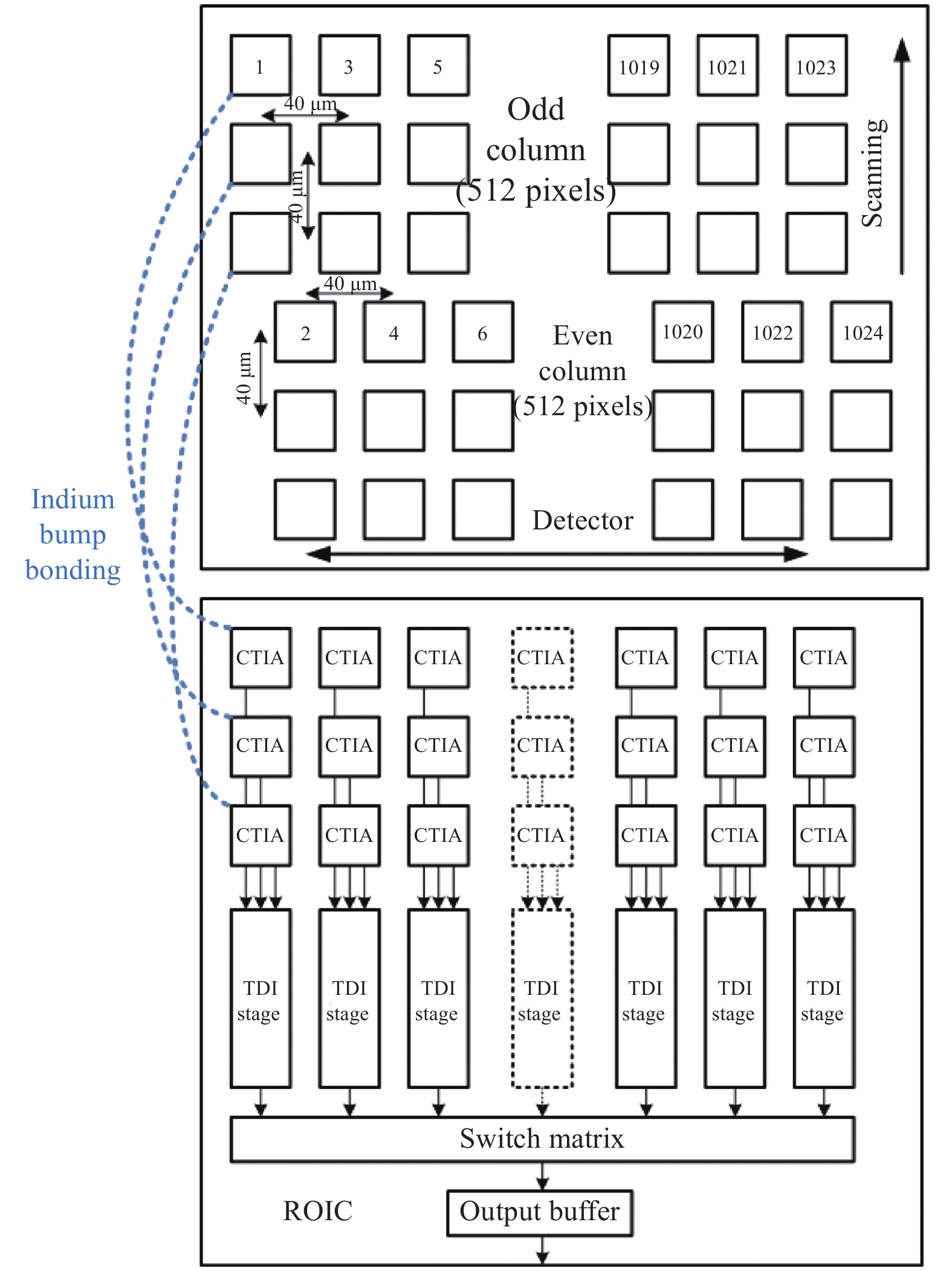
To improve the resolution of the imaging system, the infrared detector chosen for the design is arrayed as shown in Fig.1. The odd and even columns are separated and placed in two different rows, enabling the horizontal overlap between the consecutive pixels. The pixel pitch between odd and even columns is designed as width as 20 μm. Two extra rows of detectors are added vertically with a 40 μm pitch. The detector is scanned with a step of 20 μm along the scanning direction. With this configuration, a scanning type infrared detector with 1024 pixels is realized with the feasibility of implementing 3× TDI.
![]()
Figure 1.Block diagram of detector and ROIC
The detector is bonded to a readout circuit (ROIC) with an indium bump. The ROIC consists of an array of capacitor trans-impedance amplifier (CTIA) circuits located under each detector pixel, column paralleled TDI stages, switch matrix to multiplex the TDI outputs, and output buffer stage to drive the large capacitive load.
1.2 CTIA pixel stage
The CTIA architecture is chosen as the pixel circuit to convert the photocurrent into voltage for its superior linearity and detector bias stability compared to its competitor. The detailed circuit diagram is shown in Fig.2, which is comprised of one core operational transconductance amplifier (OTA), CMOS switches, and variable integration capacitor. The offset of OTA is the main source of fixed pattern noise (FPN) in the infrared image, therefore the offset cancellation technique is introduced in the design. The CTIA operates in two phases: the reset phase and the integration phase. INT and INT_N are two control clocks with opposite phases. In the reset phase, INT_N is high, the switches S1 and S2 are closed, S3 is opened. The CTIA is configured as a unity gain buffer, the integration capacitor is reset and served to store the offset of OTA. Assuming limited voltage gain as Av, the output voltage of CTIA is reset to
![]()
Figure 2.Detail circuit diagram of CTIA
Therefore, the charge stored on the left side of the capacitor can be expressed as:
When switching to the integration phase, the INT turns high, the switches S1 and S2 are opened, S3 is closed. The capacitor is connected in the feedback path between the negative input terminal and output. Neglecting the effect of charge injection and clock feedthrough, the initial output voltage of CTIA right after the switching activity can be derived from the following equation base on the charge conservation for the left plate of the integration capacitor. The formula of the charge stored and the output voltage is given by Eqs.(3) and (4).
It is convenient to get the conclusion that the offset-induced error would be greatly reduced as long as the voltage gain is large, eliminating the offset-induced FPN that would be happened in the conventional CTIA circuit.
The detector bias is held constant due to the virtual short characteristic of the feedback, facilitating the linear response of the detector. When the photocurrent produced by the detector flows through the capacitor within the integration timing window, the output voltage of CTIA will change linearly from the initial value derived in the previous equation.
For the limited pixel area as small as 40 μm×40 μm, the OTA is designed as a differential amplifier with only 5 transistors. To accommodate the large dynamic range with photocurrent, a variable integration capacitor ranging from 5 fF to 130 fF is designed. The simulated result in Fig.3 shows less than 0.3% nonlinearity, demonstrating the advantage of the chosen CTIA circuit.
![]()
Figure 3.Simulated linearity of CTIA
1.3 TDI stages
The designed TDI schematic is shown in Fig.4, where the Vi<1>-Vi<3> is the output from the previous CTIA pixel stage. As is described in the previous section, because the detector is scanned with the step of the half-pitch, the image captured by the first detector will be captured after two steps by the second detector, and four steps by the third detector. For this purpose, 5/3 capacitors are needed to sample/store the pixel output originating from the first/second detector respectively.
![]()
Figure 4.TDI schematic
The TDI circuit is also operated in two phases: sampling phase and charge transferring phase. In the sampling phase, three sampling switches are closed and all the other switches are opened, the output voltages from the CTIA pixel circuits are sampled into the storage capacitors connecting to the closed sampling switches. In the transferring switches, three specific transferring switches are closed and all the other switches are opened, the charges stored on the capacitors connecting to the closed transferring switches are averaged and transferred to the TDI output through the feedback capacitor.
To accomplish the scanning process of one image point, five steps are needed before the averaging operation can be applied for this specific point. With the detailed timing diagram in Fig.5, the needed five steps are shown as follows.
![]()
Figure 5.Timing diagram of TDI
Assuming the image point (donated as the red box in the diagram) is exposed to the first detector exactly in the first scanning step, sampling switches T11, T21 and T31 are closed, the output voltages from the three-pixel circuit are sampled on the corresponding capacitors. Specifically, the capacitor C11 captures the signal associated with the image point. The sampling switches are opened in the subsequent transfer phase, therefore the signal is frozen on the floating capacitor C11, which state is maintained for four steps until the averaging operation can be carried out.
In the second step, the sampling switches T12, T22, T31 are closed. But because the scanning step is limited to half the pixel pitch, none of the detectors can cover the image point.
In the third step, the image point is exposed to the second detector. At the same time, the sampling switches T13, T23, T31 are closed. Therefore, the signal associated with the image point can be sampled and frozen for two steps on the floating capacitor C23.
The operation in the fourth step is similar to that of the second step, except the sampling switches are changed to T14, T21, and T31.
In the fifth step, the image point is exposed to the third detector. With the closed switches of T15, T22, T31, the signal associated with the object can be sampled to the capacitor C31.
At this point, the signals sampled on the capacitor C11, C23 and C31 are available to enhance the SNR. The transferring switches TR11, TR23, and TR31 are closed, the stored signal is averaged and transferred to the TDI output.
For the next step, it is easy to infer that the signals sampled into the capacitor C12, C21, and C31 are just the right outputs resulting from the same exposed imaging point. Therefore, the averaging operation will be carried out continuously.
1.4 Output buffer
The output buffer is necessary to drive the highly resistive and capacitive load within the limited time for the multiplexed TDI output. As the TDI outputs are varied from different stages, the large-signal behavior, or slew rate characteristic is of importance for the output buffer.
To decrease the settling time, there are two feasible approaches. One can choose to increase the static bias current, or choose the push-pull output structure. The latter technique is adopted for the low power consideration. The simplified schematic is shown in Fig.6.
![]()
Figure 6.Simplified diagram of output buffer
2 Measurement Result
Part of the chip layout is shown in Fig.7. The chip was fabricated with a 0.35 μm CMOS process and occupies an area of 1.3 mm×20 mm. With the 5 V power supply, the power consumption is less than 60 mW.
![]()
Figure 7.Odd and even column layout of ROIC
To validate the CTIA pixel circuit, one external resistor is connected to the input, converting the applied voltage into the current. Fig.8 shows the voltage output directly from the CTIA circuit, it is clear to distinguish the reset phase and integration phases.
![]()
Figure 8.Captured output voltage from CTIA pixel circuit
To validate the TDI stages, three different voltages are injected into the terminals Vi<1>, Vi<2>, and Vi<3>.Tab.1 summarizes the different combinations of three voltages and TDI output voltage. The averaging operation is realized successfully under all conditions.
| Input 1/V | Input 2/V | Input 3/V | Output/V |
| 0.5 | 0.5 | 1 | 0.66 |
| 0.8 | 0.8 | 1 | 0.86 |
| 1 | 1 | 1 | 0.99 |
| 1.2 | 1.2 | 1 | 1.13 |
| 1.5 | 1.5 | 1 | 1.16 |
Table 1. Injected input & captured output from TDI stage
3 Conclusion
In this paper, a 1024×3 TDI readout circuit is proposed and implemented. This readout circuit consists of capacitor trans-impedance amplifier (CTIA) pixel circuits, paralleled TDI stages, multiplexer, and output buffer. The chip was manufactured with a 0.35 μm CMOS process and occupies an area of 1.3 mm×20 mm. With the 5 V power supply, the power consumption is less than 60 mW. The measurement results validate the proposed design successfully.
References
[1] C C Hsieh, C Y Wu, F W Jih, . et al. Focal-plane-arrays and CMOS readout techniques of infrared imaging systems. IEEE Transactions on Circuits and Systems for Video Technology, 7, 594-605(1997).
[2] Byunghyuk Kim, Hee Chul Lee. Smart TDI readout circuit for long-wavelength IR detector. Electronics Letters, 38, 854-855(2002).
[3] H Hanamura, M Aoki, T Masuhara, et al. Operation of bulk CMOS devices at very low temperatures. IEEE Journal of Solid-State Circuits, 21, 484-490(1986).
[4] Tsai Fukai, Huang Hongyi, Dai Likuo, et al. A timedelayintegration CMOS readout circuit f IR scanning[C]International Conference on Electronics, Circuits Systems, 2002, 1: 347350.
[5] Sizov F F, Derkach Y P, Kononenko Y G, et al. Readout device processing electronics f IR linear focal plane arrays[C]Proceedings of SPIE, 1999, 3698: 816825.
[6] Chen L P, Hewitt M J, Gulbransen D J, et al. Overview of advances in highperfmance ROIC designs f use with IRFPAs[C]Proceedings of SPIE, 2000, 4028: 124138.
[7] R G Carvajal, J Ramírez-Angulo, A J López-Martín, et al. The flipped voltage follower: A useful cell for low-voltage low-power circuit design. IEEE Transactions on Circuits and Systems I : Regular Papers, 52, 1276-1291(2005).
[8] M Yavari. Single-stage class AB operational amplifier for SC circuits. Electronics Letters, 46, 977-979(2010).
[9] Kayahan Huseyin, Yazici Melik, Ceylan Omer, et al. Design of ROIC based on switched capacit TDI f MCT LWIR focal plane arrays[C]Proceedings of SPIE, 2011, 8012: 80120M.
[10] Ceylan Omer, Kayahan Huseyin, Yazici Melik, et al. Design of 90×8 ROIC with pixel level digital TDI implementation f scanning type LWIR FPAs[C]Proceedings of SPIE, 2013, 8704: 870432.
[11] Huseyin Kayahan, Omer Ceylan, Melik Yazici, et al. Wide range, process and temperature compensated voltage controlled current source. IEEE Transactions on Circuits and Systems I: Regular Papers, 60, 1345-1353(2013).


Set citation alerts for the article
Please enter your email address

© Copyright 2018-2021 | Chinese Laser Press. All Rights Reserved 沪ICP备15018463号-20