
Li Zhang, Haitao Qi, Hongjuan Cheng, Lei Jin, Yuezeng Shi. Preparation and characterization of AlN seeds for homogeneous growth[J]. Journal of Semiconductors, 2019, 40(10): 102801
- Journal of Semiconductors
- Vol. 40, Issue 10, 102801 (2019)
Abstract
1. Introduction
AlN single crystal is a promising semiconductor material with the largest direct band gap, high breakdown voltage, good thermal conductivity, thermal stability and chemical stability. Compared with SiC substrate or sapphire substrate, AlN crystal has smaller mismatches with GaN and AlxGa1–xN epitaxial layers in lattice structure and expansion coefficient, which can be an ideal substrate for GaN and AlxGa1–xN based UV-C LED, high-voltage and high-power devices and solar-blind detections[
Method for preparing AlN single crystal mainly focused on physical vapor transport (PVT) due to high growth velocity and low dislocation density. In 1976, Slack et al. firstly developed sublimation technique and grew centimeter-scale AlN crystal in tapered tungsten crucible by spontaneous nucleation. Other research organizations[
Because SiC crystal has the same hexagonal structure and has a small mismatch in the a-axis lattice constant with AlN crystal, more and more scientists have paid more attention on SiC seeds for AlN growth. Otherwise, SiC crystal has other excellent features such as high melting point, highly stable and large size, which is an ideal seed for AlN growth. Nitride Crystal, LMU University and Erlangen University, etc.[
Generally, there are two ways to obtain AlN seed. One way for AlN seed is from AlN crystal ingots grown SiC seeds[
2. Experimental process
Crystal growth experiment was carried out in a self-made radio-frequency induction heating furnace. Before growth experiment, thermal field distribution of growth crucible was simulated, which could help us design the configuration of thermal zone and obtain moderate convex temperature distribution. In addition, the process of seed fixed was optimized to reduce the probability of seed back-sublimation, while thermal zone structures (graphite, TaC crucible and felt insulation) was prepared strictly to increase used life and reduce the impurity in system. AlN polycrystalline source was placed at the bottom of TaC crucible, while self-made on-axis 4H-SiC seed was fixed on the crucible cap by glycosyl binder. Optimized parameters (supersaturation at the growth interface, growth temperature and growth pressures at different growth stage) were used in the growth process. Growth temperature was set at the range of 1830–2020 °C, while growth pressure at the range of 500–900 mbar, the distance between AlN polycrystalline source and SiC seed was 40 mm. Different growth strategies were used at different stages of AlN single crystal growth process by adjusting the relative positions of induction coil and crucible. For example, we adopted the strategy of lower seed temperature and higher pressure to suppress the deposition of SiC seed at the initial stage of growth. At the same time, a larger axial temperature gradient can accelerate the sublimation of AlN source and condensation on the SiC seed, which could further protect the integrity of SiC seed. Similarly, we adopted different growth parameters at the growth stages depending on the cognition of growth processes and growth experiences.
Crystallization performance of AlN wafers were characterized by delta-X type high resolution X-Ray diffractometer of Bruker corporation and HR800 type Raman spectroscopy at the wavelength from 100 to 1000 cm–1 in X(Z-Z)Y direction using the 488 nm laser for excitation. Concentration and distribution of impurities such as silicon, carbon, and oxygen were measured by secondary ion mass spectrometry (SIMS). AlN wafer was placed in a KOH/NaOH melt for 3 min and the dislocation density was counted under a scanning electron microscopy (SEM). Roughness of AlN wafer was investigated by AFM.
3. Results and discussion
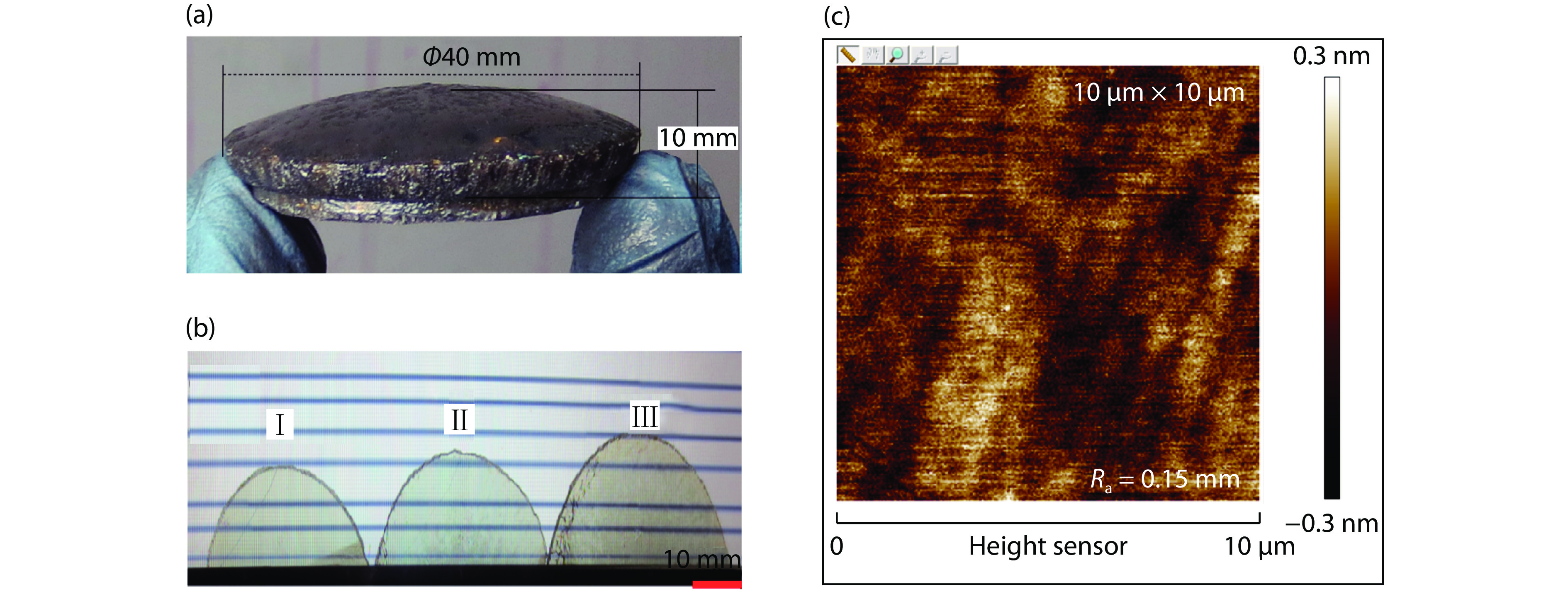
AlN crystal with diameter of about 40 mm and thickness of about 10 mm has been grown on SiC seed, as shown in Fig. 1(a). As-grown surface of AlN crystal is slightly convex with lots of hexagon tiny pits. No cracks are investigated in AlN crystal (shown in Fig. 1(a)) under bright light, when it is taken out of the furnace. However, there are two cracks in the wafers after the AlN crystal is sliced by the diamond wire with low slicing speed. The appearance of cracks may be due to the external force by the diamond wire or the internal force existed in the AlN single crystal which can’t easily be detected. The two cracks exist in the slicing wafers without separation. However, the wafers are divided into three parts after polishing process, halves of which are shown in Fig. 1(b), named sample I, II, and III, respectively. Sample I is close to the growth surface, sample III is close to the AlN-SiC interface and sample II is between the above-mentioned two. Three samples were transparent and almost colorless with increasing diameters from 30 to 40 mm due to the thermal field distribution and convex growth. Roughness of AlN polished samples were at the level of 0.15 nm shown in Fig. 1(c).
![]()
Figure 1.(Color online) (a) AlN single crystal. (b) AlN samples. (c)
Raman spectroscopy of AlN single crystal samples was shown in Fig. 2. It can be seen from Fig. 2(a) that the Raman peaks of three samples are located at the wavenumber of 247, 657 and 891 cm–1, which are corresponded to E2(low), E2(high) and A1(LO) phonon modes, indicating AlN samples are typical c-plane growth. Raman mapping mode were subjected to the samples (not shown here) indicating good uniformity of c-axis orientation. E2 (high) phonon mode peaks of three samples in Fig. 2(b) are high-intensity and sharp, indicating good crystallization quality. Moreover, FWHM values of E2 (high) phonon mode peak are gradually decreased from sample III to sample I, which means the improved crystallization quality during the growth process. However, the peak positions of E2 (high) phonon mode in three samples are slightly lower than 657.4 cm–1, which means tensile stress still exists in the samples. Compared with the peak position in sample I, the other two samples are modestly blue-shifted. It can be deduced that the tensile stress are gradually decreased during the growth process.
![]()
Figure 2.(Color online) Raman spectrum of AlN samples. (a) Wavelength from 100 to 1000 nm. (b) Detailed
It can be seen from the HRXRD of AlN samples in Fig. 3 that diffraction curves of symmetrical (0002) plane and asymmetric (
![]()
Figure 3.(Color online) HRXRD of AlN samples (a) (0002) plane and (b) (
Crystallization performance of AlN samples improves with the growth process from the results of Raman and HRXRD measurements, which may be related with the growth mechanism of AlN crystals grown on SiC heterogeneous seeds, as shown in Fig. 4.
![]()
Figure 4.(Color online) Schematic diagrams of AlN single crystal grown on Si-polar SiC seed. (a) SiC macroscopic steps and deposited AlN 3D islands. (b) AlN 3D islands lateral overgrowth and dislocation formation. (c, d) Cavity movement and dislocation "annihilation".
Because the Si-polar plane has the lowest corrosion rate[
In order to count the TD density, three AlN samples are etched in KOH/NaOH melt solution at 320 °C for 3 min, which are shown in Fig. 5. TD density decrease from 2.5 × 105 cm–2 of sample III to 6.5 × 104 cm–2 of Sample I for 250× magnification in SEM image, which is in coincident with dislocation "annihilation" in the growth mechanism of Fig. 4.
![]()
Figure 5.SEM images of AlN samples etched in KOH/NaOH melt solution at 320 °C for 3 min. (a) Sample I. (b) Sample II. (c) Sample III.
4. Conclusion
AlN single crystal with diameter of 40 mm has been grown on SiC heterogeneous seed. The growth mechanism on SiC seed include the following steps: SiC macroscopic steps formation, AlN 3D islands deposition, islands lateral overgrowth, dislocation formation, cavity movement and dislocation "annihilation", which can be used to account for the improved crystallization performance with AlN growth process. Sample I has high crystallization quality with (0002) and (
Acknowledgment
This work was supported by National Key Research and Development Plan of China (No. 2017YFB0404103), National Natural Science Foundation of China (No. 51702297) and Tianjin Science and Technology Plan Project (No. 17YFZCGX00520).
References
[1] W J Wang, S B Zuo, H Q Bao et al. Effect of the seed crystallographic orientation on AlN bulk crystal growth by PVT method. Cryst Res Technol, 46, 455(2011).
[2]
[3]
[4] B M Epelbaum, M Bickermann, A Winnacker. Approaches to seeded PVT growth of AlN crystals. J Cryst Growth, 275, 479(2005).
[5] C Hartmann, A Dittmar, J Wollweber et al. Bulk AlN growth by physical vapour transport. Semicond Sci Technol, 29, 084002(2014).
[6] C Hartmann, J Wollweber, A Dittmar et al. Preparation of bulk AlN seeds by spontaneous nucleation of freestanding crystals. Jpn J Appl Phys, 52, 08JA06(2013).
[7] H I Helava, E N Mokhov, O A Avdeev et al. Growth of low-defect SiC and AlN crystals in refractory metal crucibles. Mater Sci Forum, 740–742, 85(2013).
[8] R R Sumathi, M Paun. Growth of (0001) AlN single crystals using carbon-face SiC as seeds. Mater Sci Forum, 740–742, 99(2013).
[9] R R Sumathi, P Gille. Role of SiC substrate polarity on the growth and properties of bulk AlN single crystals. J Mater Sci: Mater Electron, 25, 3733(2014).
[10] M Bickermann, B M Epelbaum, O Filip et al. Deep-UV transparent bulk single-crystalline AlN substrates. Phys Status Solidi, C7, 1743(2010).
[11] R R Sumathi, P Gille. Development and progress in bulk
[12] R R Sumathi. Bulk AlN single crystal growth on foreign substrate and preparation of free-standing native seeds. Cryst Eng Commun, 15, 2232(2013).
[13] L J Schowalter, G A Slack, J B Whitlock et al. Fabrication of native, single-crystal AlN substrates. Phys Status Solidi, C7, 1997(2003).
[14] S B Schujman, L J Schowalter, R T Bondokov et al. Structural and surface characterization of large diameter, crystalline AlN substrates for device fabrication. J Cryst Growth, 310, 887(2008).
[15] R Dalmau, H S Craft, J Britt et al. High quality AlN single crystal substrates for AlGaN-based devices. Mater Sci Forum, 924, 923(2018).
[16] R R Sumathi, R U Barz, T Straubinger et al. Structural and surface topography analysis of AlN single crystals grown on 6H–SiC substrates. J Cryst Growth, 360, 193(2012).
[17] C Hartmannn, M Albrecht, J Wollweber et al. SiC seed polarity-dependent bulk AlN growth under the influence of residual oxygen. J Cryst Growth, 344, 19(2012).
[18] I Nagai, T Kato, T Miura et al. AlN bulk single crystal growth on 6H-SiC substrates by sublimation method. J Cryst Growth, 312, 2699(2010).

Set citation alerts for the article
Please enter your email address
© Copyright 2018-2021 | Chinese Laser Press. All Rights Reserved 沪ICP备15018463号-20