Guo-Hao JU, Zheng-Xi CHENG, Yong-Ping CHEN. Lateral linear mode avalanche photodiode through 0.35 μm high voltage CMOS process[J]. Journal of Infrared and Millimeter Waves, 2022, 41(4): 668
Copy Citation Text
This letter reports on a lateral linear mode avalanche photodiode through 0.35 μm high voltage CMOS process. The linear mode avalanche photodiode is designed and fabricated with the lateral separate absorption, charge and multiplication (SACM) structure using an epitaxial wafer. The DNTUB layer, DPTUB layer, Pi layer and SPTUB layer are used for the lateral SACM structure. This improves freedom of the design and fabrication for monolithic integrated avalanche photodiode without high voltage CMOS process modifications. The breakdown voltage for the lateral linear mode avalanche photodiode is about 114.7 V. The dark currents at gain M = 10 and M = 50 are about 15 nA and 66 nA, respectively. The effective responsive wavelength range is 450 ~ 1050 nm. And the peak responsive wavelength is about 775 nm at 20 V while M = 1. With unity gain (M = 1), the responsivity at 532 nm is about half of the maximum.
Optical detection of visible and near-infrared(NIR)radiation(λ < 1100 nm)has been focused on various developments of silicon avalanche photodiodes(APDs). APD is a semiconductor photodetector in which a photon carrier can be generated due to photoelectric effect of solid-state semiconductor material[1]. The avalanche multiplication of carriers can be triggered by the photon-generated carrier in strong electric field due to an impact-ionization mechanism[2]. The separate absorption,charge and multiplication(SACM)silicon APD[3-4] is a very attractive device with an internal avalanche gain for supporting high sensitivity and low illumination detection. It is also highly desirable to fabricate silicon APDs together with electronic circuits in a cost-effective and less-parasitic single-chip[5-6] through high voltage CMOS process without process modifications.
However,with the limitations of design rules for most CMOS process,it is extremely difficult to achieve a suitable charge layer which is used to modulate the electric field in multiplication region for the vertical SACM APDs. Until now,most commercial SACM APDs have not been able to meet the requirements of low-cost,high-performance,monolithic integration and large-scale arrays. And only units APD or small-scale linear array APD can be fabricated and available. In order to design and fabricate vertical SACM APD through CMOS process without any process modification there are two design approaches which are usually carried out to get a suitable charge layer. The first way is the transverse space doping modulation. The groups have designed several silicon APDs by applying lateral well modulation[7-8]. The other method is the compensation doping modulation. Some silicon APDs were designed by combining different doping process layers[9]. For most lateral structure silicon APDs,the ordinary lateral p-n junction is adopted with p type and n type doping[10-12].
In this letter,we report the fabrication and characterization of lateral linear mode avalanche photodiode based on 0.35 μm high voltage CMOS process without any technology rules modification. This linear mode APD is fabricated with the lateral SACM structure using the 15 μm thick epitaxial layer. The photosensitive surface is an octagonal region[13] which is partially covered with electrode metal and shielding metal. In the next section,the structure and fabrication of the APD will be introduced. Then,in Sect. 2,the APD will be characterized and discussed,including current,gain,breakdown voltage and responsivity. In Sect.3,the conclusion of this work is given.
1 Device structure and fabrication
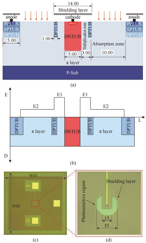
The cutaway schematic(not to scale)of the lateral SACM APD presented in this paper is seen from Fig. 1(a). As shown in Fig. 1(a),the linear mode APD is designed with lateral SACM structure including DNTUB(Deep-N-TUB)layer,DPTUB(Deep-P-TUB)layer,Pi(π)layer and SPTUB(Shallow-P-TUB)layer. The regular DNTUB layer and DPTUB layer for modulating electric field distribution are fabricated in 0.35 μm high voltage CMOS technology. The multiplication zone of such structure is between the central DNTUB layer and loop-locked DPTUB layer. As shown in Fig. 1(b),this structure can ensure that the lateral electric field strength in absorption zone is much lower than that in the multiplication zone,thus to confine the avalanche to the multiplication zone. The high doping concentration of the top NPLUS layer and PPLUS layer can form ohmic contact with the front metal electrodes. Meanwhile,the top NPLUS layer and PPLUS layer supply voltage to the DNTUB layer and Pi layer. The SPTUB layer and DPTUB layer connected to the PPLUS layer serve as the transition layer. Except for the absorption zone surface,the other surfaces are covered with a separate metal layer to shield incident light. The shielded multiplication zone can effectively reduce the participation of holes generated from incident light absorption in avalanche process.
Figure 1.Schematic views of APD (a) cross section, (b) simplified electric field distribution, (c) the microscopic picture of the complete APD device, (d) the microscopic picture of the photosensitive region (Unit: μm)
Figures 1(c)and(d)are the microscopic picture of the complete lateral SACM APD device and the microscopic picture of the photosensitive region,respectively. The size of the complete APD device is 910 μm×910 μm. Excluding the center electrode,the area of the active octagonal photosensitive region is 618 μm2. The size of the PAD is 100 μm×100 μm. The metal M3 layer and M4 layer are used as shielding layer and the top electrode,respectively.
2 Results and discussions
2.1 Current and gain
The light current and dark current of the lateral APD are measured through Keithley 4200A-SCS Parameter Analyzer. The unity gain for M = 1 is defined at the low reverse bias voltage of 20 V. Furthermore,the breakdown voltage of the lateral APD is defined as the reverse voltages at which the dark current reaches 1 μA[14]. The photocurrent is measured using a light source with center wavelength λ = 905 nm and spectral width △λ = 3 nm. The dark current in Fig. 2 shows that the breakdown voltage of the lateral linear mode APD is at about 114.7 V. The dark currents of the lateral APD are about 15 nA and 66 nA when the typical gains are set at M = 10 and M = 50,respectively.
The photocurrent multiplication gain defined through equation(1) is shown in Fig. 3. In the following formula,Ilight represents the total current,Iph denotes the photocurrent,V represents the reverse bias voltage and V0 stands for the reference reverse bias voltage for M = 1[15]. V0 = 20 V was used for the data shown in Fig. 3. The test result indicates that the reverse bias voltage of the device is about 114 V at the typical photocurrent multiplication gain M = 50. Besides,the photocurrent multiplication gain is up to 100 at reverse bias voltage of 114.5 V.
,
Figure 3.Multiplication gain vs. reverse bias voltage
The normalized spectral responsivity for the lateral linear mode APD is obtained at the low bias voltage of 20 V with unity gain(M = 1)with the spectral responsivity test system and is shown in Fig. 4. The normalized responsive wavelength range of the device is tested to be 450~1 050 nm. The maximum responsivity wavelength of the device is about 775 nm at 20 V while M = 1. With unity gain(M = 1),the responsivity at 532 nm is about half of the maximum. As shown in Fig. 4,the spectral response curve reveals peak of interference with wavelength,which is caused by the multi passivation layers through 0.35 μm high voltage CMOS process. A black broken line is marked by fitting peaks of measured data. It shows the definite trend relationship between responsivity and wavelength(450~1 050 nm)if an anti-reflective coating(ARC)layer is fabricated through 0.35 μm high voltage CMOS process in the future.
Figure 4.Normalized responsivity vs. wavelength(450 ~ 1050 nm)
The lateral linear mode avalanche photodiode with the photo sensitive area of 618 μm2 is implemented through 0.35 μm high voltage CMOS process. The lateral SACM and DNTUB/DPTUB/Pi/SPTUB layers are adopted. The breakdown voltage is observed about 114.7 V. And the dark currents are tested to be about 15 nA and 66 nA at gain M = 10 and M = 50,respectively. The responsive wavelength range is 450 ~ 1050 nm. The maximum responsivity wavelength is about 775 nm at 20 V while M = 1. With improved anti-reflective coatings(ARC),the spectral response of the device is expected to be better.
Guo-Hao JU, Zheng-Xi CHENG, Yong-Ping CHEN. Lateral linear mode avalanche photodiode through 0.35 μm high voltage CMOS process[J]. Journal of Infrared and Millimeter Waves, 2022, 41(4): 668