Abstract
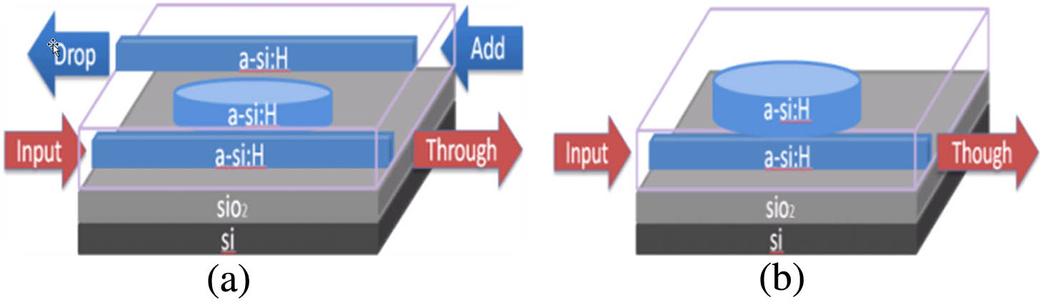
A simple method to fabricate vertically coupled micro-ring resonators in amorphous silicon-on-insulator is created by a three-step lithography process. First, the linear loss at 1.55 μm of the a-Si:H film is calculated to be . Then, the bottom line waveguide of Su-8 with a flat top surface of 300 nm is created by etching. The thickness of Su-8 can easily be controlled by the etching time. Finally, by opening the window pattern and etching several layers, the first layer marks made by electron beam lithography are found with a 50 nm resolution, and the high quality of the micro-ring resonator is demonstrated.Micro-ring resonators are a rapidly developing area of research in photonic devices with a wide range of applications, including signal-processing filters, sensors, lasers, modulators, switches, memory, and slow-light elements. Generally speaking, micro-ring resonators represent frequency-selective elements that can perform a variety of functions, such as add/drop filtering, switching, and modulating in wavelength division multiplexing systems[1]. The basic structure of micro-ring resonators consists of a ring-shaped waveguide coupled to either one or two straight optical waveguides. The ring and the bus waveguide may be positioned in the same horizontal plane (lateral coupling), or the ring can be located above the bus waveguide (vertical coupling). Vertical coupling to the resonator offers several advantages over lateral coupling: 1) First and foremost among these is that the ring/bus interaction can be controlled to a fine degree, as the vertical separation is obtained by a well-controlled deposition, rather than by etching fine gaps[2]; 2) buried waveguides suffer less from scattering loss and offer better input/output coupling; 3) finally, if the waveguides are positioned directly below the ring, the interaction strength becomes insensitive to small alignment deviations[3,4]. This last fact is beneficial, as the optimum performance is achieved when the degree of coupling of both of the bus waveguides to the ring are identical. There are two kinds of vertical coupling micro-ring resonators. In Fig. 1(a), the add/drop bus is above the input/throughput bus and the ring, which are on the same plane. The add/drop bus transforms the micro-resonator into a wavelength-selective filter that allows signals of certain wavelengths to be transferred from one waveguide port (input) to another (drop). In Fig. 1(b), the ring is above the input/throughput bus, and is coupled to a single waveguide (input/throughput).

Figure 1.Vertically coupled micro-ring resonators. (a) Four-port and (b) two-port configurations.
People often use silica, silica-on-silicon, silicon, silicon-on-insulator (SOI), silicon nitride, and oxynitride, polymers, semiconductors, and crystalline materials such as lithium niobate and calcium fluoride as materials to fabricate micro-resonators[5]. In particular SOI substrates are now widely used for making highly efficient photonic integrated circuits[6–9]. However, to be complementary metal oxide semiconductor back-end compatible, the maximum temperature of the deposition process should be restricted to 400°C. Among the three kinds of silicon (amorphous, polycrystalline, or crystalline), only amorphous silicon of high quality, low loss, low temperature (100°C–400°C), and that allows flexible multilayer stacking by plasma-enhanced chemical vapor deposition (PECVD) can be deposited[10–12]. It indicates that the propagation loss of hydrogenated amorphous silicon (a-Si:H) waveguides have approached that of their crystalline Si counterparts. In this Letter, we concentrate on the fabrication of vertically coupled micro-ring resonators in amorphous SOI materials, as depicted in Fig. 1(b). An important feature of this structure is the higher refractive index () contrast of the different materials with respect to SOI technology: a-Si:H (), silicon (), silica (), and air (). This high index contrast allows for the design of small, wavelength-scale nano-photonic structures.
Although these devices were first proposed in 1969[13], only recent technological advances have allowed for the fabrication of micrometer-sized structures with sufficiently high quality[1]. In 2009, Pafchek showed that the quasi-transverse magnetic-mode propagation loss of 1.83 dB/cm at 1565 nm was achieved in horizontal Si(amorphous)–SiO–Si(crystalline) slot waveguides with 8.3 nm slots fabricated on SOI[14]. In 2013, Lipka[15] fabricated and optically characterized horizontally coupled hydrogenated amorphous silicon photonic resonators for label-free lab-on-chip biosensors. The photonic microdisk and ring resonators were patterned with electron beam lithography (EBL) and structured with inductively coupled plasma (ICP) etching, resulting in photonic wire waveguides and disk and ring resonators with a 10 and 20 μm radius, respectively. The a-Si:H resonators exhibit loaded -factors of for both resonator types and both polarizations. Although some publications mention vertically coupled micro-ring resonators[2,16–26], almost all of them were fabricated using the optical lithography process and can be achieved by using other materials instead of a-Si:H. Furthermore, the process was very hard to process and control. Using EBL can guarantee a much higher resolution in the positioning of the top devices with respect to the bottom ones. In this Letter, we present a rather simple method with three lithography steps that all use EBL and conventional reactive-ion etching to achieve vertically coupled micro-ring resonators in amorphous SOI materials that yield high resolution, accurate dimensional control, an extremely narrow ring-to-waveguide gap of 50 nm, and smooth sidewalls of the fabricated devices.
Sign up for Chinese Optics Letters TOC. Get the latest issue of Chinese Optics Letters delivered right to you!Sign up now
We aim to deposit 200 nm of a-Si:H onto a wafer that consists of two layers: the 500 μm Si-substrate, followed by a 5 μm silica () buffer. The a-Si:H layer was deposited using a load-locked Plasmalab 100 dual-frequency PECVD system from Oxford with a maximum electrode temperature of 700°C. The H-incorporation plays an important role in passivating the dangling bonds and resulting in the low loss of the a-Si:H material. The deposition conditions are shown in Table 1.
| T (°C) | P (mTorr) | SiH4(sccm) | He (sccm) | RF power (W) | Deposition rate (nm/min) | Refractive index n |
|---|
| 250 | 1500 | 25 | 475 | 10 | 20 | 3.6 |
Table 1. Hydrogenated Amorphous Silicon Deposition Conditions
The hydrogen concentration was measured by Fourier transform infrared spectroscopy (FTIR), and the bandgap energy was determined using a Filmtek 4000 spectroscopic reflector meter. Under the above deposition condition, the film contained about 10% hydrogen and had a bandgap of 1.73 eV, which is consistent with the values reported by Fukutani et al.[27]. According to our FTIR results, which are shown in Fig. 2(a), the hydrogen in the film was mainly associated with the Si-H bonds (centered at ) rather than the (centered at ). This suggests that the film was of good quality, since Si-H passivates Si dangling bonds and has the effect of reducing the defect density, while causes extra scattering losses[28]. The linear loss at 1.55 μm of the a-Si:H wafer was measured to be by prism coupling a 1.55 μm beam coupled into the 0.2 μm thick film and recording the intensity decay of the propagating beam as it passed through the film with an InGaAs camera, as shown in Figs. 2(b) and 2(c).
Figure 2.Characterization of the material properties. (a) The FTIR spectrum. (b) The IR camera image of loss streak from a 200 nm a-Si:H wafer. (c) The data extracted from this image fitted with a linear decay.
Three-step lithography was used to fabricate the vertically coupled micro-resonator: 1) The first step uses lithography to define the waveguide and the alignment marks in the a-Si:H layer; 2) the second step uses lithography to coat a thin Su-8-resistant layer with a flat top surface and to deposit a second layer of a-Si:H. This is followed by defining large windows around the alignment marks of the first layer, followed by etching the top a-Si:H layer and the thin Su-8-resistant layer to expose the alignment marks; 3) the final step uses lithography to define the micro-resonator followed by the dry etching of the top a-Si:H layer.
All of these steps were accomplished by EBL using a RAITH 150 system. This system allows for very high-resolution scanning electron microscope imaging at an extremely low voltage, typically 1 kV. The dry etching processes were run using a load-locked ICP-reactive ion etcher (Oxford Instruments Plasmalab ICP 100). Figure 3 shows the complete process.
Figure 3.Whole lithography processes.
Figure 4.Ma-N 2405 dose testing result.
We aim to fabricate an 8 mm long straight waveguide with a set of eight alignment marks surrounding the waveguide for the first lithography and etching process. We used normal writing for the alignment marks (writing field of ), whereas we used a fixed-beam moving stage (FBMS) to define the 8 mm long straight waveguide. Unlike in normal writing, when using FBMS, the beam remains fixed in position while the stage underneath follows arbitrarily shaped paths of the desired patterns. Patterns can be several millimetres to meters long, while maintaining lateral dimensions below 20 nm up to micrometers with the lowest line edge roughness. For this step, the resist we chose is a negative tone resist named Ma-N 2405. Its advantage is that only the waveguide and alignment marks need to be exposed to the electron beam so that after development, only the exposed areas remain. Ma-N 2405 is available in a variety of viscosities, and is electron beam and deep ultraviolet-sensitive. It is quite suitable as an etching mask: it exhibits high dry and wet etch resistance, good thermal stability of the resist patterns, high-resolution capability, and aqueous alkaline development[29–31]. In this work, we used Ma-N 2405: thinner() dilution, and it was spin-coated on a-Si:H at 3000 r/min for 30 s and pre-baked at 200°C for 30 min, and then baked at 90°C for 1 min to form a 0.2 μm film. The lithography parameters were tuned before the right dose () was determined to get the 500 nm wide waveguide shown in Fig. 4. As can be seen in Fig. 5, we used a dose of and got a result of a 504.7 nm width, which is within the accepted range. We also investigated the etching parameters of a-Si:H, such as the chamber pressure, RF power (DC bias), ICP power, the ratio of flow rate of CHF3, and etching time to obtain a smooth and vertical waveguide, as shown in Fig. 6.
Figure 5.Optical microscopy picture of the first layer of a two-port ring resonator.
Figure 6.Scanning electron microscope pictures of straight waveguide, mark, and first layer of four-port racetrack resonator after etching.
For the vertical coupling, we need a polymer that can protect the first layer configuration and that is transparent. At the same time, the polymer should endure the deposition temperature of the second a-Si:H layer at 250°C. We found Su-8 to be the most appropriate polymer for this application. One of its numerous advantages is that it has very high transmission for the wavelength range above 400 nm[32]. It also exhibits relatively good chemical and thermal stability with a degradation temperature of [33]. The Su-8 layer should be able to planarize the etched waveguides to allow a smooth surface for the second EBL step. This was only possible when a 4 μm or above thick layer Su-8 was spun on the waveguide to ensure that the waveguide was properly planarized. Subsequently, the Su-8 layer was etched back until just 500 nm were left. Under the optimized etching conditions shown in Table 2, a smooth and planar surface of Su-8 was obtained.
| Su-8 Coating | Spinning rate(r/min) | Spinning t(min) | Bake T(°C) | Bake t(min) | UV light t(min) | Bake T(°C) | Bake t(min) | Thick (nm) |
|---|
| 2000 | 0.5 | 90 | 1 | 0.1 | 90 | 1 | 4600 |
| Su-8 Etching | Pressure (mTorr) | O2 (sccm) | Ar (sccm) | CHF3 (sccm) | RF power (W) | T(°C) | Deposited rate(nm/min) |
| 15 | 30 | 2 | 3 | 10 | 10 | 336 |
Table 2. Su-8 Coating and Etching Conditions
Afterwards, we deposited another 200 nm thick layer of a-Si:H. The sample was then ready for the second round of lithography. Here, we wanted to open some window roughly situated above the alignment marks defined in the first EBL step (the resolution of this is very tolerant, around several micrometers). We used a positive resist, ZEP520A, which can be used a few times until the window is above the bottom marks. We chose the ZEP520A resist due to its high resolution, high sensitivity, and high resistance to dry etching[34]. Figure 7 shows the optical microscopy photograph after development. Subsequently, the top a-Si:H layer is dry etched (200 nm), as is the 300 nm Su-8 resist, using the same etching parameters described above. Finally, we used plasma to remove the residual ZEP520A resist.
Figure 7.Optical microscopy photograph of windows pattern on bottom marks after development.
The third step of lithography again makes use of the Ma-N resist, and the micro-ring location is defined using the alignment marks defined in the first EBL step. We used the four bigger marks () to manually define a local coordinates system that is used to find the four smaller marks () automatically and to determine the location of the micro-resonator. Finally, we used the same etching process as in the first step to smoothly etch the resonator.
The loss of the bottom a-Si:H straight waveguide was determined by the cut-back method, as shown in Fig. 8. The values for the TM and TE modes were measured to be 2.6 and 3.2 dB/cm, respectively, with the higher losses for the TE mode originating from its greater sensitivity to the roughness of the etched side walls. A lensed fiber with a mode-field area of was used to couple light into and out of the nanowire, and this resulted in a total coupling loss of per facet, due mostly to the large mismatch with the fundamental mode of the waveguide, whose area was . In addition, Fig. 8 shows an example of a vertically coupled micro-ring resonator that is resonated at 1551.2 nm with , , and .
Figure 8.Micro-ring resonator testing result.
In conclusion, we describe a method to fabricate vertically coupled micro-ring or racetrack resonators in amorphous SOI using EBL. This includes the demonstration of low linear loss at 1.55 μm of the a-Si:H film. We show a successful planarization process using an Su-8 resist and demonstrate the fabrication of a vertically coupled micro-resonator and waveguides with a 50 nm lateral placement accuracy of the relative potion between the above ring and the bottom waveguide. Moreover, we can easily control the gap between the bottom waveguide and the above micro-ring by changing the etched thickness of Su-8.
References
[1] B. Radjenović, M. Radmilović-Radjenović. Int. J. Numer Model., 27, 259(2014).
[2] B. E. Little, S. T. Chu, W. Pan, D. Ripin, T. Kaneko, Y. Kokubun, E. P. Ippen. IEEE Photon. Technol. Lett., 11, 215(1999).
[3] J. Guo, M. J. Shaw, G. A. Vawter, P. Esherick, G. R. Hadley, C. T. Sullivan. Proceedings of 17th Annual Meeting IEEE/LEOS.2, 745(2004).
[4] L. Yang, W. Pan, L. Yan, B. Luo, P. Mu, N. Li. Chin. Opt. Lett., 13, 41403(2014).
[5] J. Heebner, R. Grover, T. A. Ibrahim. Optical Microresonators—Theory, Applications and Fabrication, 35(2008).
[6] P. Dumon, G. Priem, L. R. Nunes, W. Bogaerts, D. Van Thourhout, P. Bienstman, T. K. Liang, M. Tsuchiya, P. Jaenen, S. Beckx, J. Wouters, R. Baets. Jpn. J. Appl. Phys., 145, 6589(2006).
[7] B. Schmidt, Q. F. Xu, J. Shakya, S. Manipatruni, M. Lipson. Opt. Express, 15, 3140(2007).
[8] Z. Sheng, D. X. Dai, S. L. He. J. Lightwave Technol., 25, 3001(2007).
[9] F. N. Xia, L. Sekaric, Y. Vlasov. Nat. Photon., 1, 65(2007).
[10] L. Liao, D. R. Lim, A. M. Agarwal, X. M. Duan, K. K. Lee, L. C. Kimerling. J. Electron. Mater., 29, 1380(2000).
[11] S. K. Selvaraja, E. Sleeck, M. Schaekers, W. Bogaerts, D. V. Thourhout, P. Dumon, R. Baets. Opt. Commun., 282, 1767(2009).
[12] A. Harke, M. Krause, J. Mueller. Electron. Lett., 41, 1377(2005).
[13] E. Marcatili. Bell Syst. Tech. J., 48, 2103(1969).
[14] R. M. Pafchek, J. Li, R. S. Tummidi, T. L. Koch. IEEE Photon. Technol. Lett., 21, 353(2009).
[15] T. Lipka, L. Wahn, H. K. Trieu, L. Hilterhaus, J. Müller. J. Nanophoton., 7, 073793(2013).
[16] S. Suzuki, K. Shuto, Y. Hibino. IEEE Photon. Technol. Lett., 4, 1256(1992).
[17] I. S. Amiri, J. Ali. Chin. Opt. Lett., 11, 041901(2013).
[18] S. T. Chu, B. E. Little, W. Pan, T. Kancko, S. Sato, Y. Kokubun. IEEE Photon. Tech. Lett., 11, 691(1999).
[19] D. V. Tishinin, P. D. Dapkus, A. E. Bond, I. Kim, C. K. Lin, J. O’Brien. IEEE Photon. Technol. Lett., 11, 1003(1999).
[20] K. J. Vahala. Nature, 424, 839(2003).
[21] Y. Hatakeyama, T. Hanai, S. Suzuki, Y. Kokubun. IEEE Photon. Technol. Lett., 16, 473(2004).
[22] Y. Kokubun, Y. Hatakeyama, M. Ogata, S. Suzuki, N. Zaizen. IEEE J. Sel. Topics Quantum Electron., 11, 4(2005).
[23] Y. Wu. Chin. Opt. Lett., 12, 110607(2014).
[24] A. Yalcin, K. C. Popat, J. C. Aldridge, T. A. Desai, J. Hryniewicz, N. Chbouki, B. E. Little, O. King, V. Van, S. Chu, D. Gill, M. Anthes-Washburn, M. S. Unlu. IEEE J. Sel. Topics Quantum Electron., 12, 148(2006).
[25] A. Madani, H. Azarinia, H. Latifi. Int. J. Light Electron Opt., 124, 1746(2013).
[26] A. Madani, S. Böttner, M. R. Jorgensen, O. G. Schmidt. Opt. Lett., 39, 189(2014).
[27] K. Fukutani, M. Kanbe, W. Futako, B. Kaplan, T. Kamiya, C. M. Fortmann, I. Shimizu. J. Non-Cryst. Solids, 63, 227(1998).
[28] R. C. Kamikawachi, I. Abe, A. S. Paterno, H. J. Kalinowski, M. Muller, J. L. Pinto. J. Opt. Commun., 281, 621(2008).
[29] V. M. N. Passaro, M. La Notte, B. Troia, L. Passaquindici, F. De Leonardis, G. Giannoccaro. Int. J. Res. Rev. Appl. Sci., 11, 411(2012).
[30] V. M. N. Passaro, C. de Tullio, B. Troia, M. La Notte, G. Giannoccaro, F. De Leonardis. Sensors, 12, 15558(2012).
[31] H. Elsner, H. G. Meyer, A. Voigt, G. Grutzner. Microelectron. Eng., 46, 389(1999).
[32] B. Yang, L. Yang, R. Hu, Z. Sheng, D. X. Dai, Q. K. Liu, S. L. He. J. Lightwave Technol., 27, 4091(2009).
[33] R. Feng, R. J. Farris. J. Mater. Sci., 37, 4793(2002).
[34] T. Nishida, M. Notomi, R. Iga, T. Tamamura. Jpn. J. Appl. Phys., 31, 4508(1992).