• Chinese Optics Letters
  • Vol. 14, Issue 5, 052201 (2016)
An Pan1, Tao Chen1、*, Cunxia Li2, and Xun Hou1
Author Affiliations
  • 1Key Laboratory for Physical Electronics and Devices of the Ministry of Education, Shaanxi Key Lab of Information Photonic Technique, School of Electronics & Information Engineering, Xi’an Jiaotong University, Xi’an 710049, China
  • 2Xi’an University of Technology, Department of Applied Physics, Xi’an 710049, China
  • show less
    DOI: 10.3788/COL201614.052201 Cite this Article Set citation alerts
    An Pan, Tao Chen, Cunxia Li, Xun Hou. Parallel fabrication of silicon concave microlens array by femtosecond laser irradiation and mixed acid etching[J]. Chinese Optics Letters, 2016, 14(5): 052201 Copy Citation Text show less
    (a) Schematic diagram of parallel fabrication process of MLAs. (b) Optical setup of multi-beam femtosecond laser irradiation showed in dashed box in (a).
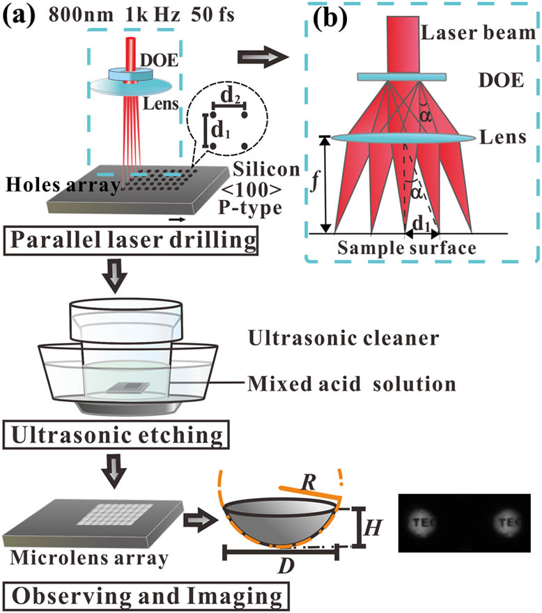
    Fig. 1. (a) Schematic diagram of parallel fabrication process of MLAs. (b) Optical setup of multi-beam femtosecond laser irradiation showed in dashed box in (a).
    Typical etched surface morphologies of laser-cut silicon in mixed acid (a) HF∶HNO3=10∶1 and (b) HF∶HNO3=1∶6 after 2 min.
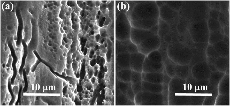
    Fig. 2. Typical etched surface morphologies of laser-cut silicon in mixed acid (a) HFHNO3=101 and (b) HFHNO3=16 after 2 min.
    Typical etched surface morphologies of laser-ablated microholes in mixed acid (a) HF∶HNO3∶HAC=3∶12∶10 and (b) HF∶HNO3∶H2SO4∶HAC=3∶12∶1∶10 after 40 min.
    Fig. 3. Typical etched surface morphologies of laser-ablated microholes in mixed acid (a) HFHNO3HAC=31210 and (b) HFHNO3H2SO4HAC=312110 after 40 min.
    (a)–(c) are MLAs fabricated at a laser pulse number of 100 and different powers (for a single microhole, the same below) of (a) 2, (b) 10, and (c) 15 mW. The etching time for (a)–(c) was 30 min. (d)–(f) are MLAs fabricated at 5 mW with different pulse numbers of (d) 100, (e) 300, and (f) 500. The etching time for (d)–(f) was 60 min. Figure 4 was captured by the optical microscopy.
    Fig. 4. (a)–(c) are MLAs fabricated at a laser pulse number of 100 and different powers (for a single microhole, the same below) of (a) 2, (b) 10, and (c) 15 mW. The etching time for (a)–(c) was 30 min. (d)–(f) are MLAs fabricated at 5 mW with different pulse numbers of (d) 100, (e) 300, and (f) 500. The etching time for (d)–(f) was 60 min. Figure 4 was captured by the optical microscopy.
    (a) SEM image of MLA fabricated at a laser power of 5 mW, a pulse number of 500, and an etching time of 60 min. The fill factor of the MLA is about 92.8%. (b) The 3D observation of the marked part in (a). (c) The cross-section profile of microlenses along the direction marked in (b).
    Fig. 5. (a) SEM image of MLA fabricated at a laser power of 5 mW, a pulse number of 500, and an etching time of 60 min. The fill factor of the MLA is about 92.8%. (b) The 3D observation of the marked part in (a). (c) The cross-section profile of microlenses along the direction marked in (b).
    Image array formed by MLA showed in Fig. 5. The inset shows the object “TEC.”
    Fig. 6. Image array formed by MLA showed in Fig. 5. The inset shows the object “TEC.”
    An Pan, Tao Chen, Cunxia Li, Xun Hou. Parallel fabrication of silicon concave microlens array by femtosecond laser irradiation and mixed acid etching[J]. Chinese Optics Letters, 2016, 14(5): 052201
    Download Citation