1Key Laboratory for Physical Electronics and Devices of the Ministry of Education, Shaanxi Key Lab of Information Photonic Technique, School of Electronics & Information Engineering, Xi’an Jiaotong University, Xi’an 710049, China
2Xi’an University of Technology, Department of Applied Physics, Xi’an 710049, China
An Pan, Tao Chen, Cunxia Li, Xun Hou. Parallel fabrication of silicon concave microlens array by femtosecond laser irradiation and mixed acid etching[J]. Chinese Optics Letters, 2016, 14(5): 052201
Copy Citation Text
A method of multi-beam femtosecond laser irradiation combined with modified etching is used for the parallel fabrication of all-silicon plano-concave microlens arrays (MLAs). The laser beam is split by a diffractive optical element and focused by a lens to drill microholes parallely on silicon. An solution is used to expand and polish laser-ablated microholes to form microlenses. Compared with the solution, the solution with can effectively reduce the etched surface roughness. The morphologies of MLAs at different laser powers and pulse numbers are observed. The image array formed by the silicon microlenses is also demonstrated.
Nowadays, many materials have been used to fabricate microlens arrays (MLAs) for important applications in light coupling and shaping[1,2], optical sensing[3], integral imaging[4], and biochemical microfluidic systems[5]. However, there are few studies on fabricating MLAs on silicon. Silicon is widely used in the semiconductor industry. Microlenses on silicon are compatible with the micro/nanofabrication technologies in integrated circuits[6]. Different from common glasses and polymers, silicon is opaque at visible light wavelengths and is transparent beyond 1.1 μm (including the optical communication window). Therefore, silicon microlenses have usually been used for infrared and terahertz devices. Silicon concave MLAs are promising in devices such as infrared diffusers[7] and scanners[8]. Besides microlenses, silicon concave spherical structures are widely used as molds to replicate polymer microlenses[9], and they can also be used as concave micro-mirrors or microcavities[10,11].
Silicon microlenses are usually fabricated via reactive-ion etching (RIE) from etching masks or resist lenses on silicon[12,13]. This method has the high precision of anisotropic etching; however, it suffers the disadvantages of etched-surface roughness and difficulty in fabricating ideal spherical surfaces. Direct writing methods such as the scanning-probe grayscale oxidation method have been used to flexibly and controllably fabricate silicon microlenses, except for their slow speed in fabricating arrays[14]. In addition, silicon concave spherical structures could also be obtained by wet etching wafers with RIE-processed or photolithographic masks or by an electrochemical etching process[9,11,15].
The femtosecond laser is a powerful tool in micro/nanofabrication and ultrafast measurements because of its high peak power, low heat effect, and internal processing ability[16–20]. Many micro-optical devices such as compound eyes, Fresnel zone plates, Dammann gratings, and fiber Bragg gratings have been fabricated by femtosecond laser pulses[21–24]. Several studies have been published on fabricating MLAs on photopolymers or glasses by femtosecond lasers in the last decade[25,26]. Recently, we fabricated plano-concave microlenses on silicon by femtosecond laser processing and wet etching[27]. The method combining femtosecond laser processing and wet etching is very flexible and convenient to realize different curvatures of surfaces on silicon. Compared with the RIE method, this maskless method can improve the fill factor and the sphericity of the MLAs greatly. Compared with laser direct writing to form curved surfaces, laser dotting combined with wet etching is much faster and easier. However, the laser-ablated microholes were produced one by one on silicon, which indicated a relatively low efficiency. Additionally, the wet etching process, which containing hydrofluoric acid (HF), nitric acid (), and acetic acid (HAC), resulted in a relatively bad average surface roughness. In this study, we parallely fabricated MLAs with low surface roughness by combining the irradiation of diffractive optical element (DOE) -split femtosecond laser beams[28,29] and an improved mixed acid etching process. Assisted by a DOE, the femtosecond laser at 800 nm was divided into five beams to produce microholes in a row on silicon simultaneously. Periodic arrays of microholes were fabricated parallely. We have found that the etched surface roughness of the MLAs was affected greatly by different compositions of the mixed acid solution. The etched surface quality could be further improved by adding sulfuric acid () into the conventional etchant containing HF, , and HAC. This is because sulfuric acid helps the acid solution to produce and maintain the intermediate oxidants such as nitrosyl ()[30]. The specimen was put into the mixed acid solution containing HF, , , and HAC, and the microholes on the specimen were expanded and smoothed by isotropic acid etching to form concave MLAs. The silicon was first oxidized by , and the silicon oxides were removed by HF subsequently. We have observed the influence of acid compositions on the etched surface roughness and parallely fabricated MLAs at different laser powers and pulse numbers. The optical image array formed by the MLA was demonstrated. The method in this study could be used to fabricate silicon MLAs for infrared applications with highly efficient laser processing and a better silicon isotropic etching performance.
Sign up for Chinese Optics Letters TOC. Get the latest issue of Chinese Optics Letters delivered right to you!Sign up now
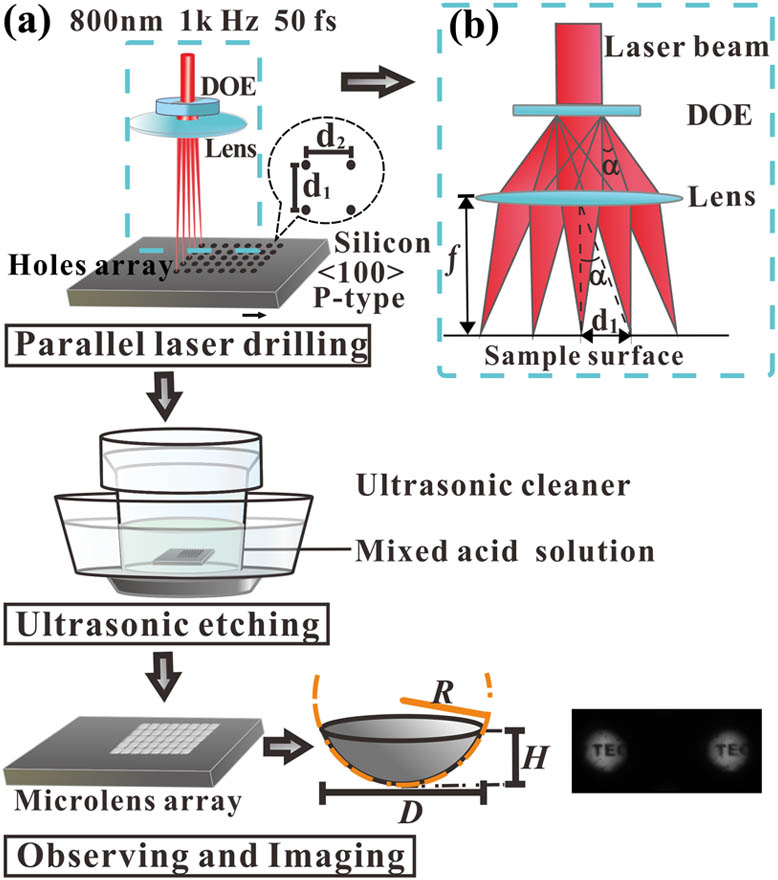
Two main steps were adopted for the parallel fabrication of MLAs on silicon, as shown in Fig. 1(a). The microhole arrays were first ablated by the split femtosecond laser, and the microholes were then etched by the mixed acid solution.
Figure 1.(a) Schematic diagram of parallel fabrication process of MLAs. (b) Optical setup of multi-beam femtosecond laser irradiation showed in dashed box in (a).
The main components of the parallel laser processing system are a femtosecond laser source, a laser control system (containing mirrors, a variable attenuator, and a mechanical shutter), a DOE, a focusing lens, and a computer-controlled xyz stage. The 800 nm femtosecond laser pulses with a repetition rate of 1 kHz, a maximum energy of 4 mJ, and a duration of 50 fs were generated by a regeneratively amplified Ti: sapphire laser system. The pulse energy and pulse number in the experiment were controlled by a variable optical attenuator and a fast mechanical shutter in front of the DOE. Figure 1(b) shows the beam splitting caused by the DOE and the beam focusing caused by the lens. The DOE has a diffraction efficiency of 74.9% and a small diffraction angle measured as 2.02 mrad. To ensure the uniformity of the five points, the DOE was designed with an energy difference of 5 beams less than 1% of the incident energy. The focusing lens (with a focal length ) was used to focus the laser tightly on the silicon. The 500 μm-thick silicon wafer was fixed on the xyz stage with a precision of 16 nm in the and directions and 3 nm in the direction. The computer-controlled stage would ensure the laser focus and irradiation on the upper surface of the silicon wafers. In one laser irradiation step, five microholes were ablated simultaneously. Subsequently, microholes in a periodic array were fabricated by laser ablation row by row.
After laser irradiation, the silicon wafer was cleaned by acetone, alcohol, and deionized water for 15 min each. Then the wafer was ultrasonically etched by a mixed acid solution in a fume cupboard at room temperature. The mixed acid solution consisted of HF (40 wt. %), (69 wt. %), (98 wt. %), and HAC (99 wt. %), and the volume ratio of these four acids was . By using ultrasonic etching, these four acids could be mixed fully and the reaction products could be removed from the sample surface in a timely manner, which could improve the uniformity of the etching process. In the etching process, the microholes were expanded into concave spherical microlenses. , , and in Fig. 1(a) denote the height, diameter, and radius of curvature of the microlenses. The two-dimensional (2D) and three-dimensional (3D) morphologies of the microlenses were characterized by an optical microscope, scanning electron microscopy (SEM), and confocal microscopy (OLS4000 Olympus) in our experiment. The surface roughness was measured by an atomic force microscope (AFM, NT-DMT, P74H-PRO). Assisted by a high-sensitivity CCD camera fixed on the optical microscope imaging system, the image array formed by the MLA was shown as well.
The mixed acid solution containing HF and is usually used as anisotropic etchant of silicon in the manufacturing industry[31,32]. In the etching process, silicon is first oxidized by concentrated , and the oxide layer can be subsequently removed by HF. The reactions can be explained as follows:
Studies show that different ratios of HF to result in different etched surface morphologies. We have etched the laser-cut silicon surfaces by HF-rich and -rich solutions and the results are shown in Figs. 2(a) and 2(b), respectively. Two contrary surface morphologies appeared in the HF-rich and -rich solutions. This could be attributed to etch rate differences at different parts of the silicon. According to Kulkarni and Erk[32], the etch rate was decided by the transport and kinetic effects of etchant. In HF rich solution the etching was highly dependent on kinetic effect. The etching could show local anisotropy at regions with different activation energies. When the concentration of HF was high, irregular pores and streaks appeared on the etched surface; thus, the surface tends to be rough, as shown in Fig. 2(a). However, in solutions with high and low HF concentrations, the etching process was greatly determined by the diffusion of . It was easier for to diffuse to the microstructure’s peak than to the valley. The etch rate at the top was higher than that at the bottom. The -rich solution had a polishing effect on the etched surface, as shown in Fig. 2(b).
Figure 2.Typical etched surface morphologies of laser-cut silicon in mixed acid (a) and (b) after 2 min.
For flat silicon with laser-induced microholes in our experiment, the laser-formed wrinkles in the microholes could be smoothed out by the -rich solution. Moreover, the and values of the microholes would increase and the value would decrease. The microholes tended to become microlenses with spherical profiles. This resulted from the etch rate difference between the outside part and the inside part of the microholes. In this study, concentrated was added to HF and to improve the etched surface quality. This strong acid helps the acid solution to produce and maintain the intermediate oxidants such as nitrosyl ()[30]. The average roughness was reduced, as shown in Figs. 3(a) and 3(b). In the solution containing , the etched surface could have a root mean square roughness of 6.8 nm (measured by the AFM), which was lower than that of silicon in the acid solution without (measured as 16.1 nm), referring to the roughness of commercial polished silicon (measured as 1.1 nm). In addition, HAC was used in our experiment as an inhibiter to improve the controllability of etching and compel the generated bubbles to leave the surface.
Figure 3.Typical etched surface morphologies of laser-ablated microholes in mixed acid (a) and (b) after 40 min.
We fabricated MLAs at different laser powers and pulse numbers to study the influence of the laser processing parameters on the MLAs. The morphologies are shown in Fig. 4. Figures 4(a)–4(c) (the left-hand side of Fig. 4) and 4(d)–4(f) show MLAs fabricated at increasing laser powers and pulse numbers, respectively. In Fig. 4(a), the microlenses have a value of 40.66 μm and an value of 2.94 μm, and in Fig. 4(c) the and values are 68.67 and 16.45 μm, respectively. The value and value also increased from 55.33 μm ( value) and 1.78 μm ( value) in Fig. 4(d) to 149.89 μm ( value) and 30.90 μm ( value) in Fig. 4(f). The and values of the microlenses increased with the increase of the incident laser power and the pulse number. The increasing values contribute to the increase in the values. However, the increasing values cause the values to decrease. The experimental results showed that the values of the microlenses decreased accordingly with the increasing laser power and pulse number. The values ranged from 68.79 μm in Fig. 4(a) to 39.98 μm in Fig. 4(c) when the laser power increased, and decreased from 217.38 μm in Fig. 4(d) to 104.56 μm in Fig. 4(f) when the pulse number increased. The , , and values of the microlenses are related to the morphologies of the laser-ablated microholes. Generally, higher laser powers and pulse numbers resulted in microholes with bigger diameters and heights; therefore, the microlenses etched from those microholes have bigger and values. In this study, the laser processing efficiency increased 5 times because the DOE split the laser beam spatially. By using DOE elements that can split the laser into more beams, such as a DOE and so on, the femtosecond laser fabrication efficiency can be improved further.
Figure 4.(a)–(c) are MLAs fabricated at a laser pulse number of 100 and different powers (for a single microhole, the same below) of (a) 2, (b) 10, and (c) 15 mW. The etching time for (a)–(c) was 30 min. (d)–(f) are MLAs fabricated at 5 mW with different pulse numbers of (d) 100, (e) 300, and (f) 500. The etching time for (d)–(f) was 60 min. Figure 4 was captured by the optical microscopy.
In Figs. 4 and 5, the microlenses in one column correspond to the five microholes in one laser irradiation. The distance between two adjacent microlenses or microholes () was decided by the DOE and the lens, which is described as . The distance between two columns () is controlled by the xyz stage. In Fig. 4, . We fabricated ten columns in one group; thus, the microhole array had a dimension of . The dimension of the textured surface could be up to several square millimeters or even square centimeters; this was controlled by the moving range of the xyz stage. By controlling the laser irradiation and etching conditions, as well as the arrangement modes of the microholes, microlenses with different , , and values could be fabricated. After etching, microlenses were obtained with values varying from 40 to 150 μm and values varying from 1 to 40 μm. Moreover, the fill factor of the MLA could be controlled to reach almost 100%.
Figure 5.(a) SEM image of MLA fabricated at a laser power of 5 mW, a pulse number of 500, and an etching time of 60 min. The fill factor of the MLA is about 92.8%. (b) The 3D observation of the marked part in (a). (c) The cross-section profile of microlenses along the direction marked in (b).
Figure 5(a) is the SEM image of the all-silicon MLA with and . The partial 3D morphology of this MLA (with a fill factor of about 92.8%) is shown in Fig. 5(b). The cross-sectional profile of the microlenses along the direction (c) in Fig. 5(b) is shown in Fig. 5(c). The dashed line depicts the theoretical profile of a sphere with , and the solid line represents the actual profile measured by the confocal microscope. The deviation between the measured and the ideal profiles was less than 0.29% in the radial direction, and the root-mean-square deviation was calculated as 93.2 nm. In the imaging process, the light source had a central wavelength of 600 nm and the sample had a thickness of about 200 μm. A high-sensitivy CCD fixed on the microscopy imaging system helped us to capture the transmission light so that we could measure the focal length and obtain the image array of the MLA in Fig. 5. The focal plane was in front of the MLA in the incident light path. We sequentially imaged the focal plane and the bottom center of the concave surfaces. The distance between these two planes was the focal length of the MLA, measured as 36.7 μm.
Figure 6 shows the image array formed by the concave MLA. The object is the printed “TEC” on glass, and the images were erect and shrunken. The object and the image array were on the same side of the MLA. The measured image magnification was about 0.020. The positions of the object “TEC,” relative to each microlens of the MLA, were slightly different. So each microlens of the array imaged a different part of the object. The magnification could be designed and controlled according to geometrical optics.
Figure 6.Image array formed by MLA showed in Fig. 5. The inset shows the object “TEC.”
In conclusion, MLAs are fabricated by parallel multi-beam femtosecond laser drilling, combined with a modified mixed acid etching process. Assisted by the DOE, the laser beam is split and thus the processing efficiency is improved. The mixed solution of four types of acids is used to improve the average etching performance on the roughness of etched surface. The 2D and 3D morphologies of the concave spherical MLAs are observed. In addition, the image array formed by the MLA is demonstrated.
An Pan, Tao Chen, Cunxia Li, Xun Hou. Parallel fabrication of silicon concave microlens array by femtosecond laser irradiation and mixed acid etching[J]. Chinese Optics Letters, 2016, 14(5): 052201