• Laser & Optoelectronics Progress
  • Vol. 59, Issue 9, 0922030 (2022)
Ziyi Zhou1、2, Xianzi Dong1、**, and Meiling Zheng1、*
Author Affiliations
  • 1CAS Key Laboratory of Bio-Inspired Materials and Interfacial Science, Technical Institute of Physics and Chemistry, Chinese Academy of Sciences, Beijing 100190, China
  • 2School of Future Technology, University of Chinese Academy of Sciences, Beijing 101407, China
  • show less
    DOI: 10.3788/LOP202259.0922030 Cite this Article Set citation alerts
    Ziyi Zhou, Xianzi Dong, Meiling Zheng. Evolution and Application of Digital Micromirror Device Based Maskless Photolithography[J]. Laser & Optoelectronics Progress, 2022, 59(9): 0922030 Copy Citation Text show less
    References

    [1] Wang F X. The present situation and trend of lithography[J]. Microelectronics, 3, 53-56(1973).

    [2] Jain K., Jain K, Willson C, Willson C.G., Lin B.J., Lin B et al. Conduct ultrafast, high-resolution contact lithography with plasmon laser[J]. Equipment for Electronic Products Manufacturing, 12, 51-59(1983).

         等利用激元激光器进行超快、高分辨率接触式光刻[J]. 半导体设备, 12, 51-59(1983).

    [3] Li L, Zhou Q K, Gong C. The simple analysis and example on exposal mode of the mask aligner[J]. Equipment for Electronic Products Manufacturing, 41, 24-25, 30(2012).

    [4] Horiuchi T, Fujii H, Yasunaga K. Lithography onto surfaces of fine-diameter pipes using rotary scan-projection exposure[J]. Journal of Photopolymer Science and Technology, 28, 273-278(2015).

    [5] Song D Y, Wang X P. Advance of optical lithography technology[J]. Semiconductor Technology, 23, 2-5, 10(1998).

    [6] Xing F, Liao J K, Yang X J et al. Research progress of the nanoimprint technology[J]. Laser Journal, 34, 1-3(2013).

    [7] Chen G L, Tang B, Tang Z Y et al. Mixed E-beam and optical lithography for nanoscale devices[J]. Micronanoelectronic Technology, 50, 386-390(2013).

    [8] Lian J, Wang L M, Sun X C et al. Patterning metallic nanostructures by ion-beam-induced dewetting and Rayleigh instability[J]. Nano Letters, 6, 1047-1052(2006).

    [9] Wang Y W, Lu K. Analysis of the laser interference lithography[J]. Electronic Technology & Software Engineering, 149(2013).

    [10] Zhang W C, Zheng M L. Research progress of two-photon initiator with high efficiency and preparation of hydrogel microstructure in aqueous phase[J]. Chinese Journal of Lasers, 48, 0202007(2021).

    [11] Wang R R, Zhang W C, Jin F et al. Fabrication of polyaniline microstructure via two-photon polymerization[J]. Chinese Journal of Lasers, 48, 0202006(2021).

    [12] Chen J S. Non-mask lithograph technology for manufacturing diffractive micro-optical devices[J]. Micronanoelectronic Technology, 43, 351-354(2006).

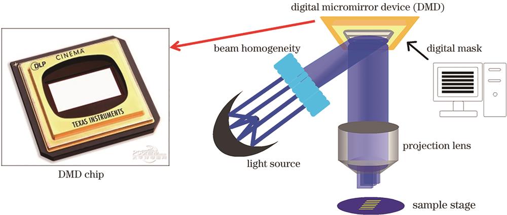
    [13] Yan W, Hu S, Tang X P et al. The method and equipment of maskless step digital lithography based on DMD[J]. Equipment for Electronic Products Manufacturing, 37, 14-19(2008).

    [14] Zhang H X, Dong L H, Wang L et al. Novel multiple exposure in fabrication of micro hemi-cylindrical lens array by digital micro mirror lithography[J]. Chinese Journal of Vacuum Science and Technology, 36, 1441-1445(2016).

    [15] Lee M P, Cooper G J T, Hinkley T et al. Development of a 3D printer using scanning projection stereolithography[J]. Scientific Reports, 5, 9875(2015).

    [16] Hornbeck L J. 128×128 deformable mirror device[J]. IEEE Transactions on Electron Devices, 30, 539-545(1983).

    [17] Douglass M. DMD reliability: a MEMS success story[J]. Proceedings of SPIE, 4980, 1-11(2003).

    [18] Hornbeck L J. Digital Light Processing and MEMS: reflecting the digital display needs of the networked society[J]. Proceedings of SPIE, 2783, 2-13(1996).

    [19] Sun C Z, Sun W S. Method of calling bitmaps stored in Microsoft Windows BMP files[J]. Application Research of Computers, 11, 29-31(1994).

    [20] Miles A, Lynn B, Blanche P A et al. 7 × 7 DMD-based diffractive fiber switch at 1550 nm[J]. Optics Communications, 334, 41-45(2015).

    [21] Wu Y H, Mirza I O, Arce G R et al. Development of a digital micromirror device-based Multishot Snapshot Spectral Imaging system[J]. Optics Letters, 36, 2692-2694(2011).

    [22] Messaoudi H, Thiemicke F, Falldorf C et al. Distortion-free laser beam shaping for material processing using a digital micromirror device[J]. Production Engineering, 11, 365-371(2017).

    [23] Zhao L X, Zhang Y D, Wang J et al. Design of spherical surface imaging projection lithography lens[J]. Opto-Electronic Engineering, 36, 93-97(2009).

    [24] Gao W, Zheng M L, Jin F et al. Fast fabrication of large-area two-dimensional micro/nanostructure by femtosecond laser[J]. Laser & Optoelectronics Progress, 57, 111421(2020).

    [25] Jiang X, Yang X, Liu H et al. DMD maskless lithography stitching error correction based on motion compensation[J]. Opto-Electronic Engineering, 47, 190387(2020).

    [26] Choi J W, Wicker R, Lee S H et al. Fabrication of 3D biocompatible/biodegradable micro-scaffolds using dynamic mask projection microstereolithography[J]. Journal of Materials Processing Technology, 209, 5494-5503(2009).

    [27] Takahashi K, Setoyama J. A UV-exposure system using DMD[J]. Electronics and Communications in Japan (Part II: Electronics), 83, 56-58(2000).

    [28] Ishikawa A. Diversion of exposure technology, born from development of spherical semiconductor. the maskless exposure apparatus[J]. Journal of Photopolymer Science and Technology, 15, 707-711(2002).

    [29] Chan K F, Feng Z Q, Yang R et al. High-resolution maskless lithography by the integration of micro-optics and point array technique[J]. Proceedings of SPIE, 4985, 37-43(2003).

    [30] Chen J S. Digital mask technology[J]. Chinese Journal of Liquid Crystals and Displays, 21, 700-703(2006).

    [31] Chen M Y, Guo X W, Ma Y Q et al. DMD-based gray-tone lithography for fabrication of continuous profile microstructure[J]. Microfabrication Technology, 18-21(2006).

    [32] Zhang L, Hu D F, Zhu P F et al. Design and improvement of DMD control methods in direct laser writing system[J]. Semiconductor Optoelectronics, 42, 741-746, 759(2021).

    [33] Zhang X L, Li Z, Gao Y Z et al. Light-driven technology based on MEMS infrared conversion films[J]. Acta Optica Sinica, 41, 1531001(2021).

    [34] Chen L S, Qiao W, Ye Y et al. Critical technologies of micro-nano-manufacturing and its applications for flexible optoelectronic devices[J]. Acta Optica Sinica, 41, 0823018(2021).

    [35] Jeong S J, Kim J E, Moon H S et al. Soft graphoepitaxy of block copolymer assembly with disposable photoresist confinement[J]. Nano Letters, 9, 2300-2305(2009).

    [36] Zhang Z M, Shen Y H, Chen H F[M]. Optics(2009).

    [37] Liu Y H, Zhao Y Y, Dong X Z et al. Limit resolution of digital mask projection lithography[J]. Chinese Journal of Quantum Electronics, 36, 354-359(2019).

    [38] Sun C, Fang N, Wu D M et al. Projection micro-stereolithography using digital micro-mirror dynamic mask[J]. Sensors and Actuators A: Physical, 121, 113-120(2005).

    [39] Yan L H, Xu R R, Gong Y Q. Technology of making chromium mask using digital photolithography system[J]. Laser & Optoelectronics Progress, 47, 120501(2010).

    [40] Lu J H, Xie X S, Zhang P Q et al. Submicron-sized optical fabrication with DMD based lithography[J]. Acta Photonica Sinica, 39, 600-604(2010).

    [41] Mills B, Feinaeugle M, Sones C L et al. Sub-micron-scale femtosecond laser ablation using a digital micromirror device[J]. Journal of Micromechanics and Microengineering, 23, 035005(2013).

    [42] Kang M S, Han C, Jeon H. Submicrometer-scale pattern generation via maskless digital photolithography[J]. Optica, 7, 1788-1795(2020).

    [43] Sommer A, Bothschafter E M, Sato S A et al. Attosecond nonlinear polarization and light–matter energy transfer in solids[J]. Nature, 534, 86-90(2016).

    [44] Wei C, Ma Y P, Han Y et al. Femtosecond laser processing of ultrahard materials[J]. Laser & Optoelectronics Progress, 56, 190003(2019).

    [45] Liu Y H, Zhao Y Y, Dong X Z et al. Multi-scale structure patterning by digital-mask projective lithography with an alterable projective scaling system[J]. AIP Advances, 8, 065317(2018).

    [46] Liu Y H, Zhao Y Y, Jin F et al. λ/12 super resolution achieved in maskless optical projection nanolithography for efficient cross-scale patterning[J]. Nano Letters, 21, 3915-3921(2021).

    [47] Liang J Y, Wu S Y, Kohn R N et al. Grayscale laser image formation using a programmable binary mask[J]. Optical Engineering, 51, 108201(2012).

    [48] Shen Y, Wu Y X, Xing Y B et al. Multi-beam maskless lithograph system[J]. Journal of Applied Optics, 31, 537-539(2010).

    [49] Choi J W, Ha Y M, Lee S H et al. Design of microstereolithography system based on dynamic image projection for fabrication of three-dimensional microstructures[J]. Journal of Mechanical Science and Technology, 20, 2094-2104(2006).

    [50] Cha C Y, Soman P, Zhu W et al. Structural reinforcement of cell-laden hydrogels with microfabricated three dimensional scaffolds[J]. Biomaterials Science, 2, 703-709(2014).

    [51] Kuang X, Wu J T, Chen K J et al. Grayscale digital light processing 3D printing for highly functionally graded materials[J]. Science Advances, 5, eaav5790(2019).

    [52] Wang D E, Wen C Y, Chang Y N et al. Ultrafast laser-enabled 3D metal printing: a solution to fabricate arbitrary submicron metal structures[J]. Precision Engineering, 52, 106-111(2018).

    [53] Praeger M, Papazoglou S, Pesquera A et al. Laser-induced backward transfer of monolayer graphene[J]. Applied Surface Science, 533, 147488(2020).

    Ziyi Zhou, Xianzi Dong, Meiling Zheng. Evolution and Application of Digital Micromirror Device Based Maskless Photolithography[J]. Laser & Optoelectronics Progress, 2022, 59(9): 0922030
    Download Citation