• Laser & Optoelectronics Progress
  • Vol. 59, Issue 9, 0922030 (2022)
Ziyi Zhou1、2, Xianzi Dong1、**, and Meiling Zheng1、*
Author Affiliations
  • 1CAS Key Laboratory of Bio-Inspired Materials and Interfacial Science, Technical Institute of Physics and Chemistry, Chinese Academy of Sciences, Beijing 100190, China
  • 2School of Future Technology, University of Chinese Academy of Sciences, Beijing 101407, China
  • show less
    DOI: 10.3788/LOP202259.0922030 Cite this Article Set citation alerts
    Ziyi Zhou, Xianzi Dong, Meiling Zheng. Evolution and Application of Digital Micromirror Device Based Maskless Photolithography[J]. Laser & Optoelectronics Progress, 2022, 59(9): 0922030 Copy Citation Text show less
    Schematic diagram of DMD maskless projection lithography
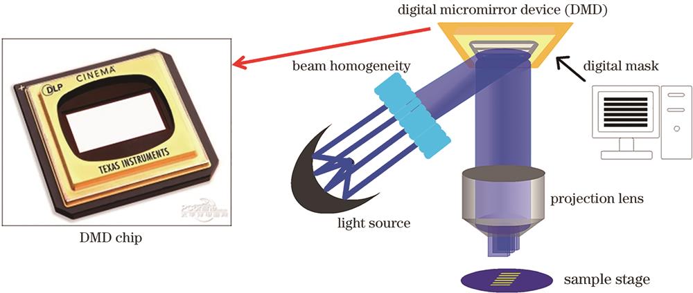
    Fig. 1. Schematic diagram of DMD maskless projection lithography
    Principle of fly-eye lens and beam homogenizer
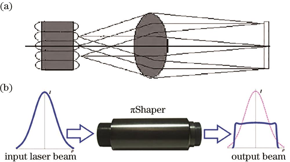
    Fig. 2. Principle of fly-eye lens and beam homogenizer
    Working principle of micromirror or micromirror array. (a) Structural diagram of single micromirror[17]; (b) scanning electron microscope image of micromirror array[17]; (c) photos of integrated DMD chips of different models[18]; (d) schematic diagram of micromirror controlling light exit direction in optical path[18]
    Fig. 3. Working principle of micromirror or micromirror array. (a) Structural diagram of single micromirror[17]; (b) scanning electron microscope image of micromirror array[17]; (c) photos of integrated DMD chips of different models18; (d) schematic diagram of micromirror controlling light exit direction in optical path[18]
    Development history of resolution of DMD maskless projection lithography. (a)~(b) 50 μm line width obtained by DMD maskless projection lithography experimentally in 2000[27]; (c)~(e) 1.5~1.8 μm horizontal scanning line width and 1 μm diagonal scanning line width obtained by point array technique projection in 2003[29]; (f) 600 nm line width obtained in 2005[38]; (g) line array of 0.67 μm width obtained in 2010[39]; (h)~(i) dot array with 900 nm period obtained in 2010[40]; (j)~(k) helix structures with 400 nm minimum linewidth in 2013[41]; (l) 357 nm feature line width obtained by introducing high NA and big magnification projection lens in 2020[42]
    Fig. 4. Development history of resolution of DMD maskless projection lithography. (a)~(b) 50 μm line width obtained by DMD maskless projection lithography experimentally in 2000[27]; (c)~(e) 1.5~1.8 μm horizontal scanning line width and 1 μm diagonal scanning line width obtained by point array technique projection in 2003[29]; (f) 600 nm line width obtained in 2005[38]; (g) line array of 0.67 μm width obtained in 2010[39]; (h)~(i) dot array with 900 nm period obtained in 2010[40]; (j)~(k) helix structures with 400 nm minimum linewidth in 2013[41]; (l) 357 nm feature line width obtained by introducing high NA and big magnification projection lens in 2020[42]
    Linewidth resolution obtained by femtosecond laser maskless surface projection exposure.(a) 150 nm feature linewidth obtained by introducing high NA objective lens and femtosecond laser[45]; (b) light field distribution diagram of single pixel width’s projection line[46]; (c) schematic diagram of chemical nonlinear effect, where left column and right column images correspond to high and low light field intensity regions in (b)[46], respectively; (d) objective lens with 100 × magnification and NA of 1.45[45], and obtained fine line array; (e) 32 nm linewidth structure which breaks through diffraction limit to λ/12[46]
    Fig. 5. Linewidth resolution obtained by femtosecond laser maskless surface projection exposure.(a) 150 nm feature linewidth obtained by introducing high NA objective lens and femtosecond laser[45]; (b) light field distribution diagram of single pixel width’s projection line[46]; (c) schematic diagram of chemical nonlinear effect, where left column and right column images correspond to high and low light field intensity regions in (b)[46], respectively; (d) objective lens with 100 × magnification and NA of 1.45[45], and obtained fine line array; (e) 32 nm linewidth structure which breaks through diffraction limit to λ/12[46]
    Photonics devices manufactured by DMD maskless projection lithography. (a)~(c) Arrayed waveguide grating pattern[46]; (d)~(e) micronanofluid device pattern[46]; (f)~(h) electrostatic comb micro-resonators[46]; (i) chromium Fresnel zone plate fabricated with single exposure[39]; (j)~(k) Fresnel zone plate with diameter of tens of micrometers, which has response at about 114 μm[45]; (l)~(m) large area structure with high precision obtained by single exposure[46]
    Fig. 6. Photonics devices manufactured by DMD maskless projection lithography. (a)~(c) Arrayed waveguide grating pattern[46]; (d)~(e) micronanofluid device pattern[46]; (f)~(h) electrostatic comb micro-resonators[46]; (i) chromium Fresnel zone plate fabricated with single exposure[39]; (j)~(k) Fresnel zone plate with diameter of tens of micrometers, which has response at about 114 μm[45]; (l)~(m) large area structure with high precision obtained by single exposure[46]
    Biological scaffolds and bionic structures fabricated by DMD maskless projection lithography. (a) Process of 3D layer-by-layer sinking fabrication[26]; (b) kidney-shaped 3D scaffold[26]; (c) top view and side view photographs of hydrogel enhanced by scaffold[50]; (d) scaffold enhanced hydrogel’s mechanical capabilities and now it can ‘stand’ on surfaces[50]; (e) bionic tendon structure inspired from human calf, capable of lifting 1 kg weight[51]
    Fig. 7. Biological scaffolds and bionic structures fabricated by DMD maskless projection lithography. (a) Process of 3D layer-by-layer sinking fabrication[26]; (b) kidney-shaped 3D scaffold[26]; (c) top view and side view photographs of hydrogel enhanced by scaffold[50]; (d) scaffold enhanced hydrogel’s mechanical capabilities and now it can ‘stand’ on surfaces[50]; (e) bionic tendon structure inspired from human calf, capable of lifting 1 kg weight[51]
    Introduction of femtosecond laser can realize exposure of special materials using DMD maskless projection lithography. (a) Processing hard material structure with layer-by-layer fabrication[52]; (b)~(c) micro metal woodpile structure and nano metal wire bridgefabricated by layer-by-layer process[52]; (d) schematic diagram of gray level represented by dot matrix density arranged uniformly in space, and simulated distribution of DMD reflected light field smoothed out by diffraction[53]; (e) graphene removed on catalysis substrate after exposure[53]; (f) graphene transferred to device substrate after exposure[53]
    Fig. 8. Introduction of femtosecond laser can realize exposure of special materials using DMD maskless projection lithography. (a) Processing hard material structure with layer-by-layer fabrication[52]; (b)~(c) micro metal woodpile structure and nano metal wire bridgefabricated by layer-by-layer process[52]; (d) schematic diagram of gray level represented by dot matrix density arranged uniformly in space, and simulated distribution of DMD reflected light field smoothed out by diffraction[53]; (e) graphene removed on catalysis substrate after exposure[53]; (f) graphene transferred to device substrate after exposure[53]
    Ziyi Zhou, Xianzi Dong, Meiling Zheng. Evolution and Application of Digital Micromirror Device Based Maskless Photolithography[J]. Laser & Optoelectronics Progress, 2022, 59(9): 0922030
    Download Citation