• Journal of Semiconductors
  • Vol. 40, Issue 2, 022802 (2019)
A. Hezabra1, N. A. Abdeslam1, N. Sengouga1, and M. C. E. Yagoub2
Author Affiliations
  • 1Laboratory of Metallic and Semiconducting Materials (LMSM), Mohammed Khider University, Biskra, Algeria
  • 2School of Electrical Engineering and Computer Science, University of Ottawa, Ottawa, ON, Canada
  • show less
    DOI: 10.1088/1674-4926/40/2/022802 Cite this Article
    A. Hezabra, N. A. Abdeslam, N. Sengouga, M. C. E. Yagoub. 2D study of AlGaN/AlN/GaN/AlGaN HEMTs’ response to traps[J]. Journal of Semiconductors, 2019, 40(2): 022802 Copy Citation Text show less
    (Color online) Cross-section of the AlGaN/AlN/GaN/AlGaN HEMT structure simulated in this work.
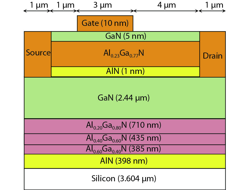
    Fig. 1. (Color online) Cross-section of the AlGaN/AlN/GaN/AlGaN HEMT structure simulated in this work.
    (Color online) Simulated (a) DC characteristics for different gate-source voltages and (b) transfer characteristics in the presence of acceptor and donor traps in the GaN channel compared to the case with no traps. Trap energy level is 0.3 eV below Ec for the acceptor and 0.3 eV above Ev for the donor.
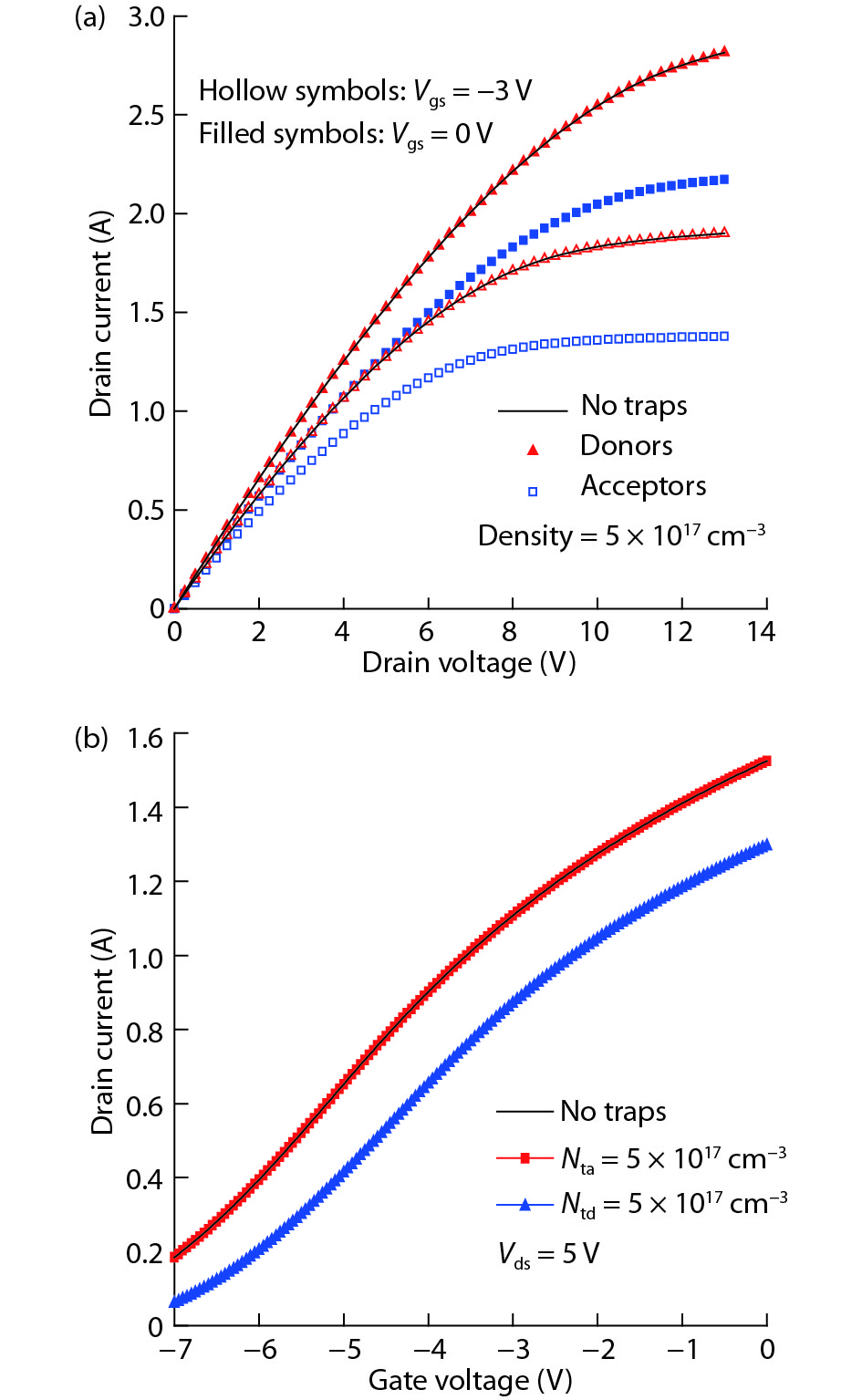
    Fig. 2. (Color online) Simulated (a) DC characteristics for different gate-source voltages and (b) transfer characteristics in the presence of acceptor and donor traps in the GaN channel compared to the case with no traps. Trap energy level is 0.3 eV below Ec for the acceptor and 0.3 eV above Ev for the donor.
    (Color online) Influence of acceptor traps located below the conductance band on the (a) output characteristics, (b) transfer characteristics, and (c) transconductance of the AlGaN/AlN/GaN/AlGaN HEMT device at Vds = 5 V. Acceptor traps in the GaN channel have a density of 5 × 1017 cm−3.
    Fig. 3. (Color online) Influence of acceptor traps located below the conductance band on the (a) output characteristics, (b) transfer characteristics, and (c) transconductance of the AlGaN/AlN/GaN/AlGaN HEMT device at Vds = 5 V. Acceptor traps in the GaN channel have a density of 5 × 1017 cm−3.
    (Color online) Influence of acceptor trap concentration on the (a) output and (b) transfer characteristics and (c) the transconductance of the device. Acceptor traps in the channel are located at Eta = 0.3 eV. The drain voltage is Vds = 5 V.
    Fig. 4. (Color online) Influence of acceptor trap concentration on the (a) output and (b) transfer characteristics and (c) the transconductance of the device. Acceptor traps in the channel are located at Eta = 0.3 eV. The drain voltage is Vds = 5 V.
    (Color online) Passivated and unpassivated structures under the same bias conditions. (a) The output and (b) transfer characteristics and (c) the transconductance of the device. Acceptor traps in the channel have a density of Nta = 5 × 1017 cm−3 and are located at Eta = 0.3 eV below the conduction band.
    Fig. 5. (Color online) Passivated and unpassivated structures under the same bias conditions. (a) The output and (b) transfer characteristics and (c) the transconductance of the device. Acceptor traps in the channel have a density of Nta = 5 × 1017 cm−3 and are located at Eta = 0.3 eV below the conduction band.
    (Color online) Influence of the temperature variations on (a) DC characteristics, (b) transfer characteristics, and (c) the transconductance of the device in the presence of acceptor traps (Nta = 5 × 1017 cm−3, Eta = 0.3 eV).
    Fig. 6. (Color online) Influence of the temperature variations on (a) DC characteristics, (b) transfer characteristics, and (c) the transconductance of the device in the presence of acceptor traps (Nta = 5 × 1017 cm−3, Eta = 0.3 eV).
    Drain current recovery curve after bias stressing with a pulse width of 1 ms on the gate (Vgs = 0, −5 V and Vds = 25 V) in the presence of acceptor-like traps (Nta = 5 × 1017 cm−3, Eta = 0.3 eV).
    Fig. 7. Drain current recovery curve after bias stressing with a pulse width of 1 ms on the gate (Vgs = 0, −5 V and Vds = 25 V) in the presence of acceptor-like traps (Nta = 5 × 1017 cm−3, Eta = 0.3 eV).
    Drain current recovery curve after bias stressing on the gate (Vgs = 0, −5 V and Vds = 10 V) in the presence of acceptor-like traps (Nta = 5 × 1017 cm−3, Eta = 0.3 eV).
    Fig. 8. Drain current recovery curve after bias stressing on the gate (Vgs = 0, −5 V and Vds = 10 V) in the presence of acceptor-like traps (Nta = 5 × 1017 cm−3, Eta = 0.3 eV).
    Material parameterGaNAlGaNAlN
    Band gap (eV)3.423.916.12
    Effective conduction band density of state (1018 cm−3) 2.242.74.42
    Relative permittivity9.58.5
    Electron affinity (eV)41.84
    Electron saturation velocity (106 cm/s) 7.515
    Table 1. Summary of the material parameters used in the simulations.
    A. Hezabra, N. A. Abdeslam, N. Sengouga, M. C. E. Yagoub. 2D study of AlGaN/AlN/GaN/AlGaN HEMTs’ response to traps[J]. Journal of Semiconductors, 2019, 40(2): 022802
    Download Citation