
A. Hezabra, N. A. Abdeslam, N. Sengouga, M. C. E. Yagoub. 2D study of AlGaN/AlN/GaN/AlGaN HEMTs’ response to traps[J]. Journal of Semiconductors, 2019, 40(2): 022802
- Journal of Semiconductors
- Vol. 40, Issue 2, 022802 (2019)
Abstract
1. Introduction
Nowadays, AlGaN/AlN/GaN high-electron mobility transistor (HEMT) technology is increasingly attracting interest from researchers due to AlGaN’s wide band gap, high electron mobility, and high breakdown voltage[
In fact, because of its higher 2DEG density, even using an ultrathin AlN barrier layer of thickness well below 5 nm, a high aspect ratio (gate length on gate-to-channel distance) can mitigate short-channel effects[
The traps may be at the surface, on the bulk or at the interface, causing effects such as current collapse, transconductance frequency dispersion, and gate- and drain-lag[
In order to provide an appropriate understanding of such effects to enable further technological advances, an analysis of trapping effects on the device performance is clearly required. In addition to this, very few analytical models have been developed to handle the high temperature effect on GaN-based devices[
To efficiently address the above issues, different directions were explored, allowing pertinent results, which will be quite useful for researchers, to be obtained. To be specific, we investigated (i) the influence of traps on the DC/RF characteristics of AlGaN/AlN/GaN/AlGaN HEMTs, such as their level within the band gap and their concentration, (ii) the effect of temperature on the device performance, (iii) how the transistor reacts when pulsed with different pulse widths, and finally (iv) the effect of passivation on the device features.
2. Simulation details and device structure
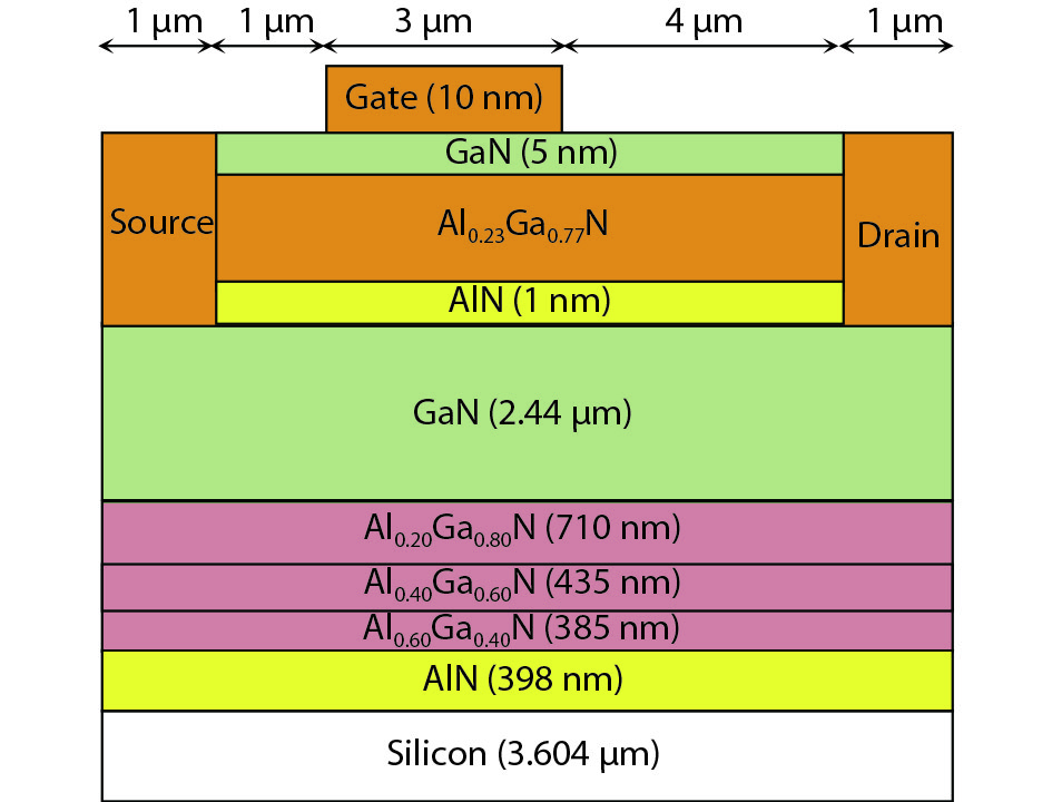
For simplicity, the investigated AlGaN/AlN/GaN/AlGaN HEMT structure has the same dimensions as the one described in Ref. [1]. As shown in Fig. 1, it consists of three thin AlxGa1-xN layers with aluminum fractions of 0.6, 0.4 and 0.2, respectively, a 2.44 µm thick GaN channel layer as buffer layer, a 1 nm ultrathin AlN barrier layer and an Al0.23Ga0.77N layer[
![]()
Figure 1.(Color online) Cross-section of the AlGaN/AlN/GaN/AlGaN HEMT structure simulated in this work.
Note that, except for the case where the temperature was varied to study its effect on the device performance, the DC simulations carried out in this work were performed at room temperature.
The TCAD-Silvaco simulations solve a system of three equations, i.e, the three fundamental equations governing the semiconductor behavior, namely the Poisson equation and the electron/hole continuity equations. Drift-diffusion (DD) transport model equations are also solved self-consistently. The software produces numerical solutions by calculating the values of the unknown variables at each grid point of the device. An internal discretization process converts the original continuous model into a discrete nonlinear algebraic system, which is then solved using an iterative process until the predefined convergence criteria are satisfied[
The processes related to generation-recombination are known to fall into six main categories, but the most frequent and dominant process is that of Shockley–Read–Hall (SRH) recombination[
The induced electric field due to the polarization phenomenon contributes to the formation of 2DEG density at the AlN/GaN interface, without the need for any intentional doping. The theoretical methods used for estimating the polarization charges are described in Ref. [16]. The polarization charge at the AlN/GaN interface is modeled as a fixed interface charge with + σpol = 1.7 × 1013 cm−2[
3. 2D simulation results
3.1. Types of traps
Two-dimensional physical-electrical simulations were performed to first determine which type of traps present in the studied heterostructure device has more influence. Fig. 2 shows the influence of acceptor traps and donors on the DC characteristics of the transistor. They decrease the drain current since they reduce the effective density of electrons in the channel while the donors do not. Knowing that the channel must be undoped in order to mitigate the scattering phenomenon, the excess electrons have enough room to diffuse because the channel is formed, in our case, by a large GaN layer. Note that these conclusions are in agreement with those reported in Ref. [2].
![]()
Figure 2.(Color online) Simulated (a) DC characteristics for different gate-source voltages and (b) transfer characteristics in the presence of acceptor and donor traps in the GaN channel compared to the case with no traps. Trap energy level is 0.3 eV below
Fig. 3 shows the influence of acceptor traps with different trap energy levels on the DC and transfer characteristics and the transconductance of the device. As can be seen, acceptor traps whose energy levels lie deep inside the band gap cause a significant drain current decrease and also a shift in the pinch-off voltage. This can also be verified by the fact that the maximum transconductance increases for deeper acceptor traps.
![]()
Figure 3.(Color online) Influence of acceptor traps located below the conductance band on the (a) output characteristics, (b) transfer characteristics, and (c) transconductance of the AlGaN/AlN/GaN/AlGaN HEMT device at
Under the biased conditions of a drain-source voltage Vds = 5 V, the trap acceptors are all ionized in the channel and thereby cause an important degradation of the drain current[
![]()
Figure 4.(Color online) Influence of acceptor trap concentration on the (a) output and (b) transfer characteristics and (c) the transconductance of the device. Acceptor traps in the channel are located at
3.2. Passivated and unpassivated cases
Passivated and unpassivated devices exhibit different increases in power dissipation at high drain bias currents. Low power dissipation is observed in unpassivated devices due to a large reduction in the output power, induced by deeper dispersion effects[
![]()
Figure 5.(Color online) Passivated and unpassivated structures under the same bias conditions. (a) The output and (b) transfer characteristics and (c) the transconductance of the device. Acceptor traps in the channel have a density of
It is well known that the surface of the material contains a large concentration of donor-like and acceptor-like traps which surpasses > 10 13 cm−2[
3.3. Temperature effect
Since temperature plays a significant role in the device performance, a study was carried out at different temperatures. Acceptor-like traps were introduced in the GaN channel with a concentration of Nta of 5 × 1017 cm− 3 and an energy level Eta of 0.3 eV below the conduction band.
As shown in Fig. 6, the drain current decreases when the temperature increases, due to the fact that the acceptor traps are ionized. In fact, increasing the temperature degrades the drain current and shifts the pinch-off voltage due to the temperature rise of the device.
![]()
Figure 6.(Color online) Influence of the temperature variations on (a) DC characteristics, (b) transfer characteristics, and (c) the transconductance of the device in the presence of acceptor traps (
3.4. Effect of pulse width
The traps-related current collapse phenomenon was also studied in this work by investigating the effect of pulse width. As shown in Fig. 7, Vgs was pulsed between 0 and −5 V while Vds was kept at 25 V. The drain current is significantly reduced, demonstrating the current collapse phenomenon. The cause of the current collapse is mainly the change in the charge state of the acceptor doping deep in the channel under the gate. For completeness, the unstressed bias remained on the device until the traps became de-populated by electrons and the drain current returned back to its original value.
Indeed, intentional doping is not necessary for GaN based devices[
![]()
Figure 7.Drain current recovery curve after bias stressing with a pulse width of 1 ms on the gate (
![]()
Figure 8.Drain current recovery curve after bias stressing on the gate (
4. Conclusion
Investigations of the electrical performance of AlGaN/AlN/GaN HEMTs grown on Si (111) substrate were carried out through 2D TCAD based numerical simulations. The results indicate an important influence of acceptor-like traps located in the channel on the DC and RF characteristics. A deeper position in the band gap under the conduction band and a larger concentration were considered, showing a significant decrease of the drain current. Meanwhile the donor-like traps show no influence. Pulsing the device with different pulse widths and bias conditions, as well as increasing temperature, showed that the traps are more ionized when the pulse is wider or the temperature higher, which can degrade the drain current, and thus the DC characteristics of the transistor.
References
[1] N Adarsh, N B Thirumaleshwara, R Saravanan et al. Effect of self-heating on electrical characteristics of AlGaN/GaN HEMT on Si (111) substrate. Advances, 7, 085015(2017).
[2]
[3] J J Zhu, X H Ma, B Hou et al. Investigation of trap states in high Al content AlGaN/GaN high electron mobility transistors by frequency dependent capacitance and conductance analysis. Advances, 4, 037108(2014).
[4]
[5] F Medjdoub, M Zegaoui, N Rolland et al. Demonstration of low leakage current and high polarization in ultrathin AlN/GaN high electron mobility transistors grown on silicon substrate. Appl Phys Lett, 98, 223502(2011).
[6] F Medjdoub, J Derluyn, K Cheng et al. Low on resistance high-breakdown normally off AlN/GaN/AlGaN DHFET on Si substrate. IEEE Electron Device Lett, 31, 111(2010).
[7] T Zimmermann, D Deen, Y Cao et al. AlN/GaN insulated-gate HEMTs with 2.3 A/mm output current and 480 mS/mm transconductance. IEEE Electron Device Lett, 29, 661(2008).
[8] Y Tang. Ultrahigh-speed GaN high-electron-mobility transistors with
[9] M Huque, S Eliza, T Rahman et al. Temperature dependent analytical model for current-voltage characteristics of AlGaN/GaN power HEMT. Solid-State Electron, 53, 341(2009).
[10] H Huq, S Islam. AlGaN/GaN self-aligned MODFET with metal oxide gate for millimeter wave application. Microelectron J, 37, 579(2006).
[11] Y Chang, Y Zhang, Y Zhang et al. A thermal model for static current characteristics of AlGaN/GaN high electron mobility transistors including self-heating effect. J Appl Phys, 99, 044501(2006).
[12] Y Chang, K Tong, C Surya. Numerical simulation of current/voltage characteristics of AlGaN/GaNHEMTs at high temperatures. Semicond Sci Technol, 20, 188(2005).
[13] S Vitanov, V Palankovski, S Maroldt et al. High-temperature modeling of AlGaN/GaN HEMTs. Solid-State Electron, 54, 1105(2010).
[14]
[15] J G Fossum, R P Mertens, D S Lee et al. Carrier recombination and lifetime in highly doped silicon. Solid-State Electron, 26, 569(1983).
[16] O Ambacher, B Foutz, J Smart et al. Two-dimensional electron gases induced by spontaneous and piezoelectric polarization charges in N-and Ga-face AlGaN/GaN heterostructures. J Appl Phys, 85, 3222(1999).
[17] K Rashmi, S Abhinav et al. An accurate charge control model for spontaneous and piezoelectric polarization dependent two-dimensional electron gas sheet charge density of lattice-mismatched AlGaN/GaN HEMTs. Solid-State Electron, 46, 621(2002).
[18]
[19] J D Albrecht, R P Wang, P P Ruden et al. Electron transport characteristics of GaN for high temperature device modeling. J Appl Phys, 83, 4777(1998).
[20] H Kim, R M Thompson, V Tilak et al. Effects of SiN passivation and high-electric field on AlGaN/GaN HFET degradation. IEEE Electron Device Lett, 24, 421(2003).
[21]
[22] J P Ibbetson, P T Fini, K D Ness et al. Polarisation effects, surface states, and the source of electrons in AlGaN/GaN heterostructure field effect transistors. Appl Phys Lett, 77, 250(2000).
[23] X G He, D G Zhao, D S Jiang. Formation of two-dimensional electron gas at AlGaN/GaN heterostructure and the derivation of its sheet density expression. Chin Phys B, 24, 067301(2015).

Set citation alerts for the article
Please enter your email address
© Copyright 2018-2021 | Chinese Laser Press. All Rights Reserved 沪ICP备15018463号-20