• Journal of Semiconductors
  • Vol. 41, Issue 12, 122403 (2020)
Jianwei Wu, Zongguang Yu, Genshen Hong, and Rubin Xie
Author Affiliations
  • The 58th Research Institute of China Electronics Technology Group Corporation, Wuxi 214035, China
  • show less
    DOI: 10.1088/1674-4926/41/12/122403 Cite this Article
    Jianwei Wu, Zongguang Yu, Genshen Hong, Rubin Xie. Design of GGNMOS ESD protection device for radiation-hardened 0.18 μm CMOS process[J]. Journal of Semiconductors, 2020, 41(12): 122403 Copy Citation Text show less
    (Color online) The structure of IC (integrated circuit) chip ESD protection system.
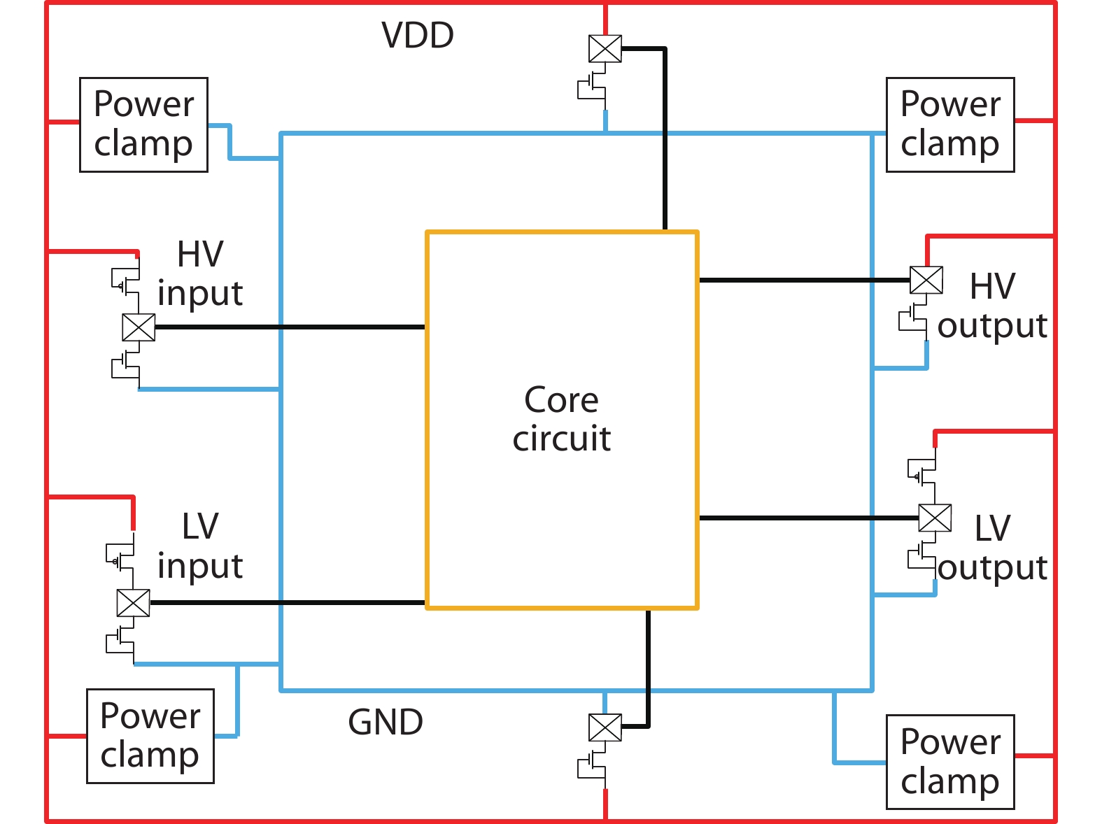
    Fig. 1. (Color online) The structure of IC (integrated circuit) chip ESD protection system.
    CMOS input and output ESD protection circuit.
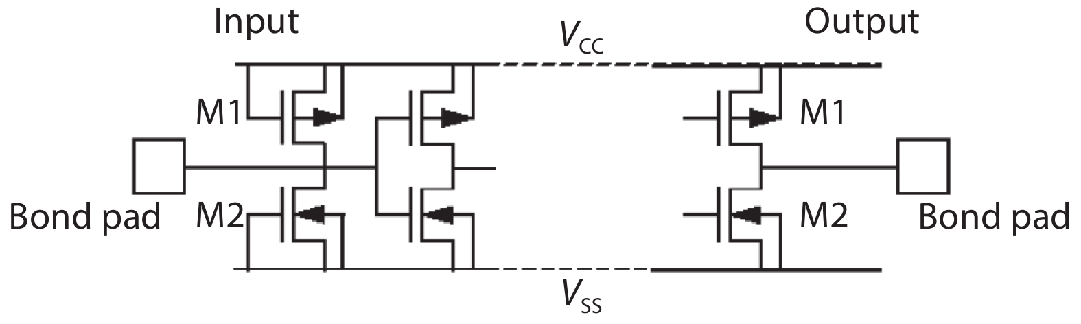
    Fig. 2. CMOS input and output ESD protection circuit.
    ESD working principle of GGNMOS device.
    Fig. 3. ESD working principle of GGNMOS device.
    (Color online) Typical discharge curve and design window of GGNMOS device in ESD event.
    Fig. 4. (Color online) Typical discharge curve and design window of GGNMOS device in ESD event.
    (Color online) (a) Structure diagram of GGNMOS. (b) 3D display of GGNMOS device.
    Fig. 5. (Color online) (a) Structure diagram of GGNMOS. (b) 3D display of GGNMOS device.
    (Color online) TCAD process simulation results of GGNMOS devices.
    Fig. 6. (Color online) TCAD process simulation results of GGNMOS devices.
    Comparison of the TCAD and test structure GGNMOS TLP curve.
    Fig. 7. Comparison of the TCAD and test structure GGNMOS TLP curve.
    (Color online) The impact ionization, current density and lattice temperature diagrams.
    Fig. 8. (Color online) The impact ionization, current density and lattice temperature diagrams.
    (Color online) The influence of gate length and DCGS on the lattice temperature of GGNMOS.
    Fig. 9. (Color online) The influence of gate length and DCGS on the lattice temperature of GGNMOS.
    (Color online) Effect of different ESD ion implantation dose on 3.3 V GGNMOS It2.
    Fig. 10. (Color online) Effect of different ESD ion implantation dose on 3.3 V GGNMOS It2.
    (Color online) Influence of single finger width on ESD current.
    Fig. 11. (Color online) Influence of single finger width on ESD current.
    (Color online) Influence of number of fingers on ESD current.
    Fig. 12. (Color online) Influence of number of fingers on ESD current.
    (Color online) Effect of DCGS size on the ESD performance of GGNMOS.
    Fig. 13. (Color online) Effect of DCGS size on the ESD performance of GGNMOS.
    (Color online) GGNMOS TLP curves with a total 240 μm width. (a) 3.3 V GGNMOS TLP It2 = 2.9 A. (b) 1.8 V GGNMOS TLP It2 = 3.84 A.
    Fig. 14. (Color online) GGNMOS TLP curves with a total 240 μm width. (a) 3.3 V GGNMOS TLP It2 = 2.9 A. (b) 1.8 V GGNMOS TLP It2 = 3.84 A.
    (Color online) EMMI of DSP circuit pad ESD fails.
    Fig. 15. (Color online) EMMI of DSP circuit pad ESD fails.
    (Color online) GGNMOS It2 value versus process nodes.
    Fig. 16. (Color online) GGNMOS It2 value versus process nodes.
    ItemFeature
    Minimum feature size0.18 μm undoped polysilicon gate
    Operating voltageCore device 1.8 V, IO device 3.3 V
    Isolation technologySTI
    Well structureDouble retrograded well
    SpacerType LONO Spacer
    Gate oxideDual gate oxide
    SilicideFully self aligned CoSi2 gate, source, drain
    InterconnectionAluminum interconnection with tungsten plug technology HDP low-K FSG IMD
    Optional deviceDN, HR, MIM optional
    Reliability≥ 20 years
    TID≥ 300 krad (Si)
    SEL≥ 75 MeV·cm2/mg
    SEU≤ 1 × 10⁻¹⁰ error /(bit·day) (with standard library)
    Table 1. The radiation-hardened 0.18 μm CMOS process characteristic parameters.
    GGNMOS deviceSingle finger width (μm) Multi finger numberTotal width (μm) Vt2 (V) It2 (A) Discharge efficiency Iesd(mA/μm) Reference
    a Indicate this work. b Published literature, Fig. 16.
    3.3 Va4062407.602.9012.08/
    1.8 Va4062408.613.8416.0/
    1.8 V40832020.274.5514.2[17]
    3.3 V606360/3 (≥ 4500 V)8.33[18]
    3.3 V3012360/1 (≥ 1500 V)2.78[18]
    3.3 V6012720/3 (≥ 8000 V)7.4[18]
    3.3 V9087205.245.177.18[19]
    1.8 V/////9.1b[1]
    3.3 V/////8.1b[1]
    Table 2. Comparison with literature.
    Jianwei Wu, Zongguang Yu, Genshen Hong, Rubin Xie. Design of GGNMOS ESD protection device for radiation-hardened 0.18 μm CMOS process[J]. Journal of Semiconductors, 2020, 41(12): 122403
    Download Citation