
Jianwei Wu, Zongguang Yu, Genshen Hong, Rubin Xie. Design of GGNMOS ESD protection device for radiation-hardened 0.18 μm CMOS process[J]. Journal of Semiconductors, 2020, 41(12): 122403
- Journal of Semiconductors
- Vol. 41, Issue 12, 122403 (2020)
Abstract
1. Introduction
With the improvement of process, the design challenges of ESD have become increasingly significant[
The radiation-hardened bulk CMOS process technology adopts an epitaxial layer technology[
The significance of this paper: through studying the working mechanism in the ESD event of GGNMOS devices, parameters such as breakdown voltage, holding voltage, internal resistance and so on are optimized. By means of device simulation, process experiment, TLP test verification and circuit ESD capability evaluation, the development and verification of the radiation hardened 0.18 μm bulk silicon CMOS process ESD protection device GGNMOS based on epitaxial wafers are completed. Without additional process steps, the ESD performance of GGNMOS can reach HBM 3500 V. The GGNMOS device has small area consumption, good robustness, excellent leakage characteristics and radiation hardness.
2. ESD protection design
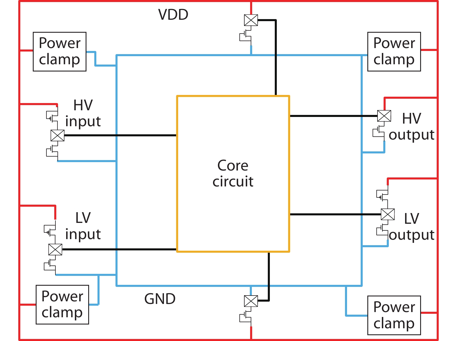
The structure of the IC (integrated circuit) chip ESD protection system is shown in Fig. 1[
![]()
Figure 1.(Color online) The structure of IC (integrated circuit) chip ESD protection system.
The typical input and output port ESD protection is shown in Fig. 2[
![]()
Figure 2.CMOS input and output ESD protection circuit.
As shown in Fig. 3, the main working principle of GGNMOS ESD device is taking advantage of NMOS device avalanche breakdown and lateral parasitic NPN (LNPN) transistor to turn on large current conduction to realize an effective method to protect the integrated circuit from damage in ESD events.
![]()
Figure 3.ESD working principle of GGNMOS device.
GGNMOS typical high current I–V curve ABCDE is shown in Fig. 4, in which the horizontal axis represents the voltage of ESD device port, the vertical axis represents its current, and the dotted line with arrow represents the ESD design window. 1) Point BVt1 is the trigger voltage of GGNMOS transverse parasitic NPN transistor, which is strongly related to the reverse biased breakdown voltage of NMOS drain PN junction. In ESD event, the reverse biased voltage of drain junction increases in a positive direction, which causes the avalanche breakdown of drain PN junction, the current flows to the substrate and body contact end, and the potential difference is formed in the body area. When the source-bulk PN junction barrier voltage drops 0.6–0.7 V, a positive bias is generated, a large number of injected electrons are quickly collected and accelerated. When the discharge coefficient is greater than 1, a positive feedback is generated, and the LNPN is triggered. 2) Point CVh is the hold voltage, which is mainly related to the body resistance. The device enters the CD section of ESD current conduction linear working area. 3) The CD segment shows a positive resistance characteristic, and large current produces lattice heating. The D point Vt2 and It2 are the secondary breakdown voltage and current, which are the key parameters for characterizing the current carrying capacity of GGNMOS devices in the ESD process. 4) When going over the D point, the gate oxide leakage, PN junction leakage and even short circuit will appear in the damaged area of GGNMOS. It is found that It2 is strongly affected by the factors of β, gate length, drain junction depth, total width (including multi index and single finger width), gate drain spacing, epitaxial layer concentration and thickness[
![]()
Figure 4.(Color online) Typical discharge curve and design window of GGNMOS device in ESD event.
3. Parameter design and process TCAD simulation of GGNMOS
In contrast from the commercial 0.18 μm bulk silicon CMOS process, the radiation hardened 0.18 μm bulk silicon CMOS process increases the total dose performance, and introduces a high concentration p+ substrate and a thin layer of p-epitaxial layer, which makes the longitudinal doping of MOSFET devices change correspondingly, and reduces the p-well resistance to inhibit the SCR single particle radiation induced latch-up. These changes affect the ESD discharge efficiency of GGNMOS devices. It is necessary to redesign the structure of GGNMOS devices to improve the robustness of devices and improve the ESD discharge ability.
In this paper, the multi-finger GGNMOS structure as shown in Fig. 5(a) below is adopted, in which AA' represents the position of 2D process simulation section, and Fig. 5(b) represents the enlarged diagram of 3D display area. On the layout, the width of single finger is W, the number of multiple fingers is M, and the gap between gate edge and drain contact is DCGS[
![]()
Figure 5.(Color online) (a) Structure diagram of GGNMOS. (b) 3D display of GGNMOS device.
In this work, TCAD simulation of polysilicon gate length, drain contact to gate-edge spacing (DCGS), ESD injection dose and TLP I–V curve in GGNMOS structure is carried out, as shown in Fig. 6. p+ sub substrate, source end, body end and gate end are connected to the cathode, while drain end is used as anode. The following curve (show in Fig. 7) is used in the electrical simulation of TLP. The TLP waveform with 10 ns rising edge, 100 ns pulse width and 10 ns falling edge is used to simulate the HBM model. Avalanche and dynamic thermal model are added to the TCAD simulation. The thermal effect simulation of ESD high current stress in the protection device is realized[
![]()
Figure 6.(Color online) TCAD process simulation results of GGNMOS devices.
![]()
Figure 7.Comparison of the TCAD and test structure GGNMOS TLP curve.
The TLP curve of GGNMOS device simulated in Fig. 7 matches with the actual test TLP curve. The Vt1 in 2D simulation is about 6.9 V, and it is similar to the measured TLP curve. the parasitic resistance of ESD discharge after LNPN startup is the same. It can be used for design and prediction of GGNMOS ESD performance.
In the TCAD simulation results shown in Fig. 8 below, the figures of three lines from top to bottom are the impact ionization, current density and lattice temperature diagrams, respectively. From left to right, it shows the situations before the AB line snap back, when the BC line snap back, after theCD line LNPN is turned on and when the D point reaches It2 as described in Section 2.
![]()
Figure 8.(Color online) The impact ionization, current density and lattice temperature diagrams.
According to the TLP simulation curve, it can be found that the trigger voltage Vt1 increases with the increase of channel length (range 0.25–1.0 μm) (variation 0.8 V). The main reason is that with the increase of L, the base length of parasitic LNPN, the current gain decreases, and the trigger voltage increases. As the amplification coefficient of parasitic LNPN decreases, more impact ionization current is needed to maintain the collector current, which leads to the high power consumption and lattice temperature of ESD devices[
In addition, when the size of DCGS increases with fixed channel length, the thermal volume is increased. Therefore when the same ESD current passes through the collector (drain), the lattice temperature is significantly reduced, which is conducive to bear more ESD current and improve the ESD performance. These results are shown in Fig. 9.
![]()
Figure 9.(Color online) The influence of gate length and DCGS on the lattice temperature of GGNMOS.
4. Experimental result
The effects of different DCGS, number of multi finger and finger width on the ESD performance of GGNMOS devices are researched, and the different ESD ion implantation dose groups are compared. Finally, the ESD performance is verified by DSP circuit.
4.1. Effect of ESD ion implantation dose on the ESD performance of GGNMOS
In Fig. 10, 6 × 10¹³, 8 × 10¹³, and 1 × 1014 cm–2 dose of ESD ion implantation are used respectively. The test structure is 240 and 480 μm 3.3 V GGNMOS with the single finger width 40 μm and DCGS 1.9 μm. Different ion implantation doses significantly affected the discharge ability of GGNMOS in ESD events. For 240 μm test structure, It2 was 1.13, 2.64, and 4.21 A, respectively, and for 480 μm test structure, It2 was 3.04, 4.34, and 5.75 A, respectively. The overall width was doubled. It means that when the width was doubled, the magnification was 2.69, 1.64, and 1.36 for different ion implantation doses.
![]()
Figure 10.(Color online) Effect of different ESD ion implantation dose on 3.3 V GGNMOS
4.2. Influence of single finger width on ESD current
Fig. 11 shows core 1.8 V and IO 3.3 V GGNMOS devices with DCGS 1.9 μm, ESD ion implantation 8 × 1013 cm–2, multi finger index 16. The value of It2 in the figure above increases with the increase of width of single finger, which is mainly due to the increase of total width and ESD discharge path. In the figure below, the normalized discharge current per unit length of ESD is 4.5 mA/μm for 3.3 V GGNMOS device when the width of single finger is 22 μm, and the maximum discharge current is 9.36 mA/μm when the width of single finger is 42 μm. The normalized discharge current per unit length of 1.8 V GGNMOS devices are basically the same in the range of single finger width 22–62 μm. All of them are above 10.0 mA/μm. Therefore, when the single finger width of GGNMOS is 42 μm, the ESD release current efficiency is the best.
![]()
Figure 11.(Color online) Influence of single finger width on ESD current.
4.3. Influence of multi finger number on the ESD performance of GGNMOS
The width of fixed single finger is 42 μm, ESD ion implantation of 6 × 1013 cm–2, the number of fingers is changed from 6, 8, 10, 12, 16, and the total width is the product of the two. As shown in Fig. 12, the ESD current of 1.8 V GGNMOS device increases linearly with the increase of the total width, and the discharge efficiency per unit length also increases gradually, reaching a maximum of 9.73 mA/μm at 16 fingers. There is a difference between 3.3 V GGNMOS and 1.8 V. When the cross index is 6, the discharge efficiency is 4.52 mA/μm, and when the cross index is 12, the maximum discharge efficiency is 9.88 mA/μm.
![]()
Figure 12.(Color online) Influence of number of fingers on ESD current.
4.4. Effect of DCGS size on the ESD performance of GGNMOS
In Fig. 13, the test structure adopts multi finger number of 6, single finger width of 40 μm, ESD ion implantation of 8 × 1013 cm–2, and DCGS of different sizes. When the DCGS value is below 2.3 μm, the discharge current of GGNMOS increases with the increase of size. When the DCGS value is above 2.3 μm, the ESD discharge current decreases with the increase of the size. When the DCGS size is equal to 2.3 μm, the discharge current reaches the maximum value, the discharge efficiency of 3.3 V GGNMOS is 12.08 mA/μm, and 1.8 V GGNMOS is 16 mA/μm. The TLP curves are shown in Fig. 14.
![]()
Figure 13.(Color online) Effect of DCGS size on the ESD performance of GGNMOS.
![]()
Figure 14.(Color online) GGNMOS TLP curves with a total 240
4.5. Integrated circuit verification
Before GGNMOS device design optimization, the ESD capability of DSP circuit in HBM mode can only reach 1000 V, EMMI positioning of crystal input pin is conducted, and it is found that ESD current is short circuited to ground GGNMOS (the red area as shown in Fig. 15). The leakage current of other input and output pins increases. After GGNMOS optimization, the ESD capacity is increased to more than 3500 V.
![]()
Figure 15.(Color online) EMMI of DSP circuit pad ESD fails.
The total ionization dose capacity of DSP circuit is verified by gamma ray, and the performance reaches 300 krad (Si). When the ESD performance is improved from 1000 to 3500 V, there is no TID degradation[
5. Analysis and discussion
With the increase of ESD ion implantation dose, the breakdown voltage of drain and body is reduced, which is conducive to the uniform opening of LNPN parasitic triode and the simultaneous opening of GGNMOS fingers[
When the width of single finger is small, the ESD capacity increases linearly with the increase of width. When it reaches 42 μm, it basically reaches the maximum value of discharge efficiency per unit size. When the width of single finger continues to increase, the ESD discharge current can continue to increase, but the increased part cannot be effectively triggered, and the comprehensive discharge efficiency shows a downward trend. Therefore, a more effective method is to mirror a GGNMOS to increase the ESD discharge capacity.
When the ESD implant dose is 6 × 1013 cm–2, and the number of multi fingers is less than 8, the robustness of GGNMOS is poor, and its ESD discharge efficiency is at a low level. The main reason is that the body contact is relatively good. After large injection, the large area source body junction cannot be forwarded. The large ESD current in the central area causes lattice burnout. When the number of multi fingers is more than 8, the area of the triggered central area increases, the ESD current per unit area decreases and more current can be released before the lattice burns down.
In the same GGNMOS device layout, compared with the traditional bulk silicon CMOS technology, the introduction of epitaxial layer increases the state of body contact and leads to the degeneration of ESD performance. In the GGNMOS structure as shown in Fig. 5(b), when the ESD event comes, the drain end will generate PN junction breakdown, and a large number of hole carriers will be injected into the body region (pwell, p-epi, p+ sub). Due to the introduction of p+ sub, the current in the z-axis direction will increase, but due to the decrease of resistance, the body potential cannot reach the previous level under the same hole carrier injection condition. In addition, the introduction of p+ sub reduces the transverse parasitic resistance, reduces the barrier voltage drop in the x-axis and y-axis direction to a range of 0.6–0.7 V (as shown in the ring area in Fig. 5(a)), and finally reduces the ability of the whole GGNMOS to release current in ESD events. By increasing the single finger width (y-axis direction), the hole carrier injection current is increased, the barrier voltage drop is increased to 0.6–0.7 V, the width near the contact area of the outer P+ ring (body in Fig. 5(b)) that can not effectively start the LNPN (as shown in the letter S in Fig. 5(a)), and the discharge efficiency of GGNMOS device is increased.
When the DCGS value increases from 1.5 μm, the reverse biased drain junction capacitance at the drain end under the forward ESD stress will increase[
Through these simulations and experimental TLP tests, it is necessary to combine the gate length, single finger width, multi finger number, DCGS, ESD ion implantation and other factors of GGNMOS. These factors are interactive and need further experimental design to optimize ESD performance. In addition, good ESD protection quality also includes several parameters that need to be considered in application, such as capacitance, leakage current, power sequencing and overvoltage conditioning etc. The ESD device or clamp should not have too much capacitance that it violates the loading limits of the I/O signaling specification. It must not draw excessive current at either high or low input or output levels. In addition, it must be compatible with normal sequence for applying power, and it can survive for a period of time under the condition of over voltage. Therefore, test structures for benchmarking the ESD robustness of different CMOS process, so as to get an excellent ESD capability.
Compared with the ESD performance of GGNMOS devices found in the relevant literature, the performance of GGNMOS devices finally achieved in this work has achieved a good level, the discharge efficiency of 3.3 V GGNMOS is 12.08 mA/μm, and 1.8 V GGNMOS is 16 mA/μm. The details are shown in Table 2.
6. Conclusion
The ESD performance of GGNMOS protection device is affected by many factors such as layout[
Acknowledgements
This work was supported by the Military Quality Engineering of China (No. 1807WR0002).
![]()
Figure 16.(Color online) GGNMOS
References
[1]
[2] R B Xie, X M Ji, J W Wu. Research on ESD performance of devices in radiation hardening process. Microprocessors, 40, 1(2019).
[3]
[4] L Z Zhang, Y Wang, Y Z Wang et al. Insight into multiple-triggering effect in DTSCRs for ESD protection. J Semicond, 38, 075001(2017).
[5] X W Bi, H L Liang, X F Gu et al. Design of novel DDSCR with embedded PNP structure for ESD protection. J Semicond, 36, 124007(2015).
[6]
[7] Y X Jiang, J Li, F Ran et al. Influence of layout parameters on snapback characteristic for a gate-grounded NMOS device in 0.13-
[8] T Y Chen, M D Ker. Analysis on the dependence of layout parameters on ESD robustness of CMOS devices for manufacturing in deep-submicron CMOS process. IEEE Trans Semicond Manuf, 16, 486(2003).
[9]
[10] B Krabbenborg, R Beltman, P Wolbert et al. Physics of electro-thermal effects in ESD protection devices. J Electrost, 28, 285(1992).
[11]
[12] M D Ker, T Y Chen. Substrate-triggered technique for on-chip ESD protection design in a 0.18-
[13] D X Wu, L L Jiang, H Fan et al. Analysis on the positive dependence of channel length on ESD failure current of a GGNMOS in a 5 V CMOS. J Semicond, 34, 024004(2013).
[14]
[15] M Paul, C Russ, B S Kumar et al. Physics of current filamentation in ggNMOS devices under ESD condition revisited. IEEE Trans Electron Devices, 65, 2981(2018).
[16] Y Wang, G Y Lu, Y Z Wang et al. Power-rail ESD clamp circuit with parasitic-BJT and channel parallel shunt paths to achieve enhanced robustness. IEICE Trans Electron, E100.C, 344(2017).
[17] L Li, K H Zhu. ESD performance analysis of gate grounded NMOS devices. Electron Pack, 11, 18(2011).
[18]
[19] Z G Li, S G Yue, Y S Sun. GDNMOS design for ESD protection in submicron CMOS VLSI. 2009 Asia Pacific Conference on Postgraduate Research in Microelectronics & Electronics, 432(2009).
[20] J Shi. Deep sub-micron ESD GGNMOS layout design and optimization. MATEC Web Conf, 198, 04009(2018).
[21]

Set citation alerts for the article
Please enter your email address
© Copyright 2018-2021 | Chinese Laser Press. All Rights Reserved 沪ICP备15018463号-20