[1] S Wirths, R Geiger, den von, G Mussler, T Stoica, et al. Lasing in direct-bandgap GeSn alloy grown on Si. Nat Photon, 9, 88-92(2015).
[2] den von, D Stange, D Rainko, I Povstugar, P Zaumseil, et al. Advanced GeSn/SiGeSn group IV heterostructure lasers. Adv Sci, 5, 1700955(2018).
[3] J Margetis, YY Zhou, W Dou, PC Grant, B Alharthi, et al. All group-IV SiGeSn/GeSn/SiGeSn QW laser on Si operating up to 90 K. Appl Phys Lett, 113, 221104(2018).
[4] SY Lin, XZ Zheng, J Yao, SS Djordjevic, JE Cunningham, et al. Efficient, tunable flip-chip-integrated III-V/Si hybrid external-cavity laser array. Opt Express, 24, 21454-21462(2016).
[5] D Liang, G Roelkens, R Baets, JE Bowers. Hybrid integrated platforms for silicon photonics. Materials, 3, 1782-1802(2010).
[6] C Zhang, SJ Zhang, JD Peters, JE Bowers. 8 × 8 × 40 Gbps fully integrated silicon photonic network on chip. Optica, 3, 785-786(2016).
[7] ZC Wang, B Tian, M Pantouvaki, WM Guo, P Absil, et al. Room-temperature InP distributed feedback laser array directly grown on silicon. Nat Photon, 9, 837-842(2015).
[8] ZC Wang, Gasse van, V Moskalenko, S Latkowski, E Bente, et al. A III-V-on-Si ultra-dense comb laser. Light Sci Appl, 6, e16260(2017).
[9] 2017 Conference on Lasers and Electro-Optics Europe & European Quantum Electronics Conference (IEEE, 2017); http://doi.org/10.1109/CLEOE-EQEC.2017.8086366.
[10] S Wirths, BF Mayer, H Schmid, M Sousa, J Gooth, et al. Room-temperature lasing from monolithically integrated GaAs microdisks on silicon. ACS Nano, 12, 2169-2175(2018).
[11] S Mauthe, NV Triviño, Y Baumgartner, M Sousa, D Caimi, et al. InP-on-Si optically pumped microdisk lasers via monolithic growth and wafer bonding. IEEE J Sel Top Quantum Electron, 25, 8300507(2019).
[12] SM Chen, W Li, J Wu, Q Jiang, MC Tang, et al. Electrically pumped continuous-wave III–V quantum dot lasers on silicon. Nat Photon, 10, 307-311(2016).
[13] AY Liu, C Zhang, J Norman, A Snyder, D Lubyshev, et al. High performance continuous wave 1.3
[14] YT Wan, J Norman, Q Li, MJ Kennedy, D Liang, et al. 13 μm submilliamp threshold quantum dot micro-lasers on Si. Optica, 4, 940-944(2017).
[15] ST Liu, XR Wu, D Jung, JC Norman, MJ Kennedy, et al. High-channel-count 20 GHz passively mode-locked quantum dot laser directly grown on Si with 4.1 Tbit/s transmission capacity. Optica, 6, 128-134(2019).
[16] YT Wan, S Zhang, JC Norman, MJ Kennedy, W He, et al. Directly modulated single-mode tunable quantum dot lasers at 1.3 μm. Laser Photon Rev, 14, 1900348(2020).
[17] YT Wan, JC Norman, YY Tong, MJ Kennedy, W He, et al. 1.3 μm quantum dot-distributed feedback lasers directly grown on (001) Si. Laser Photon Rev, 14, 2000037(2020).
[18] D Jung, R Herrick, J Norman, K Turnlund, C Jan, et al. Impact of threading dislocation density on the lifetime of InAs quantum dot lasers on Si. Appl Phys Lett, 112, 153507(2018).
[19] S Matsuo, K Takeda, T Sato, M Notomi, A Shinya, et al. Room-temperature continuous-wave operation of lateral current injection wavelength-scale embedded active-region photonic-crystal laser. Opt Express, 20, 3773-3780(2012).
[20] S Matsuo, T Fujii, K Hasebe, K Takeda, T Sato, et al. Directly modulated buried heterostructure DFB laser on SiO2/Si substrate fabricated by regrowth of InP using bonded active layer. Opt Express, 22, 12139-12147(2014).
[21] T Fujii, T Sato, K Takeda, K Hasebe, T Kakitsuka, et al. Epitaxial growth of InP to bury directly bonded thin active layer on SiO2/Si substrate for fabricating distributed feedback lasers on silicon. IET Optoelectron, 9, 151-157(2015).
[22] 2018 Optical Fiber Communication Conference (OSA, 2018); http://doi.org/10.1364/ofc.2018.th3b.2
[23] 2019 Optical Fiber Communications Conference and Exhibition (IEEE, 2019); http://doi.org/10.1364/ofc.2019.m4a.3
[24] 2017 Conference on Lasers and Electro-Optics Pacific Rim (IEEE, 2017); http://doi.org/10.1109/CLEOPR.2017.8119024.
[25] GK Periyanayagam, T Nishiyama, N Kamada, Y Onuki, K Shimomura. Lasing characteristics of 1.2 μm GaInAsP LD on InP/Si substrate. Phys Status Solidi (A), 215, 1700357(2018).
[26] 2019 24th OptoElectronics and Communications Conference (OECC) and 2019 International Conference on Photonics in Switching and Computing (IEEE, 2019); http://doi.org/10.23919/PS.2019.8818102.
[27] H Sugiyama, K Uchida, X Han, GK Periyanayagam, M Aikawa, et al. MOVPE grown GaInAsP/GaInAsP SCH-MQW laser diode on directly-bonded InP/Si substrate. J Cryst Growth, 507, 93-97(2019).
[28] 2018 IEEE Photonics Conference (IEEE, 2018); http://doi.org/10.1109/IPCon.2018.8527345
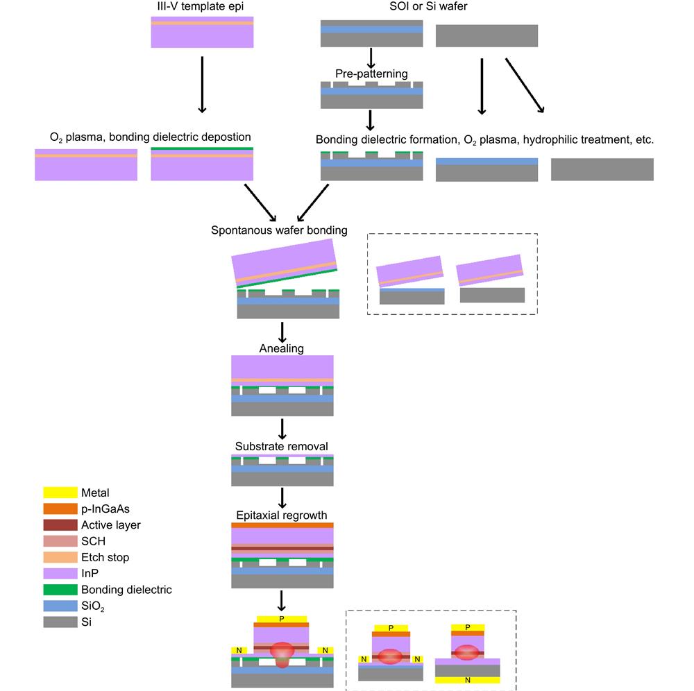
[29] YT Hu, D Liang, K Mukherjee, YL Li, C Zhang, et al. III/V-on-Si MQW lasers by using a novel photonic integration method of regrowth on a bonding template. Light Sci Appl, 8, 93(2019).
[30] YT Hu, D Liang, G Kurczveil, RG Beausoleil. A bonded template-assisted monolithic integration platform. Proc SPIE, 11184, 111840O(2019).
[31] C Besancon, N Vaissiere, C Dupré, F Fournel, L Sanchez, et al. Epitaxial growth of high-quality AlGaInAs-based active structures on a directly bonded InP-SiO2/Si substrate. Phys Status Solidi (A), 217, 1900523(2020).
[32] C Besancon, G Cerulo, D Néel, N Vaissiere, D Make, et al. Comparison of AlGaInAs-based laser behavior grown on hybrid InP-SiO2/Si and InP substrates. IEEE Photon Technol Lett, 32, 469-472(2020).
[33] D Liang, X Huang, G Kurczveil, M Fiorentino, RG Beausoleil. Integrated finely tunable microring laser on silicon. Nat Photon, 10, 719-722(2016).
[34] JC Norman, D Jung, ZY Zhang, YT Wan, ST Liu, et al. A review of high-performance quantum dot lasers on silicon. IEEE J Quantum Electron, 55, 2000511(2019).
[35] 2020 European Conference on Optical Communications (IEEE, 2020); http://doi.org/10.1109/ECOC48923.2020.9333230.
[36] K Matsumoto, J Kishikawa, T Nishiyama, T Kanke, Y Onuki, et al. Room-temperature operation of GaInAsP lasers epitaxially grown on wafer-bonded InP/Si substrate. Appl Phys Express, 9, 062701(2016).
[37] 2017 Conference on Lasers and Electro-Optics (IEEE, 2017); http://doi.org/10.1364/CLEO_AT.2017.JTu5A.108.
[38] 2018 Optical Fiber Communications Conference and Exposition (IEEE, 2018); http://doi.org/10.1364/ofc.2018.w3f.4.
[39] 2017 Conference on Lasers and Electro-Optics Pacific Rim (IEEE, 2017); http://doi.org/10.1109/CLEOPR.2017.8118971.
[40] C Zhang, JE Bowers. Silicon photonic terabit/s network-on-chip for datacenter interconnection. Opt Fiber Technol, 44, 2-12(2018).
[41] R Huang, T Lan, C Li, J Li, ZY Wang. Investigation of the blistering and exfoliation mechanism of GaAs wafers and SiO2/Si3N4/GaAs Wafers by He+ and H+ implantation. Crystals, 10, 520(2020).