
Yingtao Hu, Di Liang, Raymond G. Beausoleil. An advanced III-V-on-silicon photonic integration platform[J]. Opto-Electronic Advances, 2021, 4(9): 200094-1
- Opto-Electronic Advances
- Vol. 4, Issue 9, 200094-1 (2021)
Abstract
Introduction
With global data traffic growing exponentially, the electrical interconnects have hit a brick wall to satisfy the huge demand of high speed, energy-efficient and cost-effective data transmission in next-generation data centers, high-performance computers, and many emerging applications. By leveraging the mature complementary metal oxide semiconductor (CMOS) manufacturing processes, silicon (Si) photonics has experienced blooming developments over the past 20 years. It now holds the great promise to overcome the data transmission bottleneck problem by providing fast, reliable, and low-cost optical links. However, due to the intrinsic nature of indirect bandgap of Si material, a laser source on Si is the key challenge for Si photonics. Approaches by engineering group IV materials or their alloys have resulted in Ge and Ge-alloy (GeSi and GeSn) lasers on Si
More recently, an advanced heterogeneous integration approach by combining the advantages of direct monolithic epitaxy and wafer bonding approaches has gained increasing research interest. By using wafer bonding to bring InP-based active material onto a Si substrate and then epitaxially growing InP onto the bonded III-V material to bury the pre-defined mesa, researchers from NTT have developed a lateral p-i-n for lateral-current-injection heterostructure membrane laser
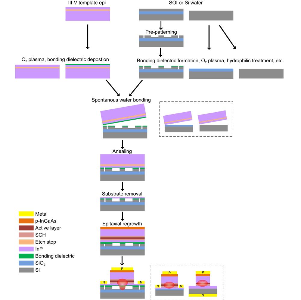
Development of III-V-on-Si bonding templates
The development of III-V-on-Si bonding templates for regrowth is basically a III-V-to-Si wafer bonding process. As the epitaxy temperature of III-V material is normally as high as 650 °C, only a direct wafer bonding technology may be suitable for such regrowth template preparation while the adhesive bonding, e.g., DVS-BCB bonding, is not as the decomposition temperature of most of the suitable polymers, which is much lower than the epitaxy temperature. Demonstrations of bonding templates from different research groups are all based on direct wafer bonding with some slight differences between each other. Figure 1 is a schematic drawing to summarize the major process steps to form such a vertical p-i-n diode laser structure on Si. We highlight the differences in bonding techniques, epitaxy and post-epi fabrications from different research groups.
![]()
Figure 1.
The Si substrate could be pure Si or SOI wafer while the later provides the possibility to create Si waveguides or other silicon photonic structures under the III-V template layer. To realize photonic structures in Si underneath the III-V template layer, pre-patterning on the SOI wafer is necessary before the wafer bonding. In our work, we also patterned vertical outgassing channels (VOC) in Si to avoid bonding defect formation, i.e., gas voids, due to gas product as a result of polymerization reactions at bonding interface. III-V Lab used a 200 nm thermal oxide on top of Si wafer as a hydrogen reservoir to allow diffusion of gas product and subsequently improve bonding quality. While there is no patterns or oxide layer in Sophia University’s bonding method but both Si substrate and template wafer underwent a hydrophilic treatment by H2SO4 cleaning. The III-V template epitaxy wafer basically includes a bonding layer and a etch stop layer on a native substrate. For the InP based templates, the bonding layer is InP and is normally n-doped to act as a contact layer of an active device. The InGaAs etch stop layer is used to selectively etch off InP substrate in the HCl-based solution, and then result in an ideal surface for regrowth once it is selectively removed. After both top surfaces of Si/SOI and III-V template wafers are cleaned and activated with O2 plasma, bonding dielectric deposition or H2SO4 solution treatment, the III-V wafer is bonded to Si/SOI wafers. By applying pressure and annealing at 300 – 400 °C, strong covalent bonds are formed. The next is to remove the III-V substrate and etch stop layer. Upon selectively removing the etch stop layer to expose the n-InP template layer, the bonding template is ready for epitaxial regrowth. The pictures from left to right in Fig. 2 show the fabricated InP-on-Si bonded wafers from our work, III-V Lab and Sophia University’s work, respectively. We carried out the bonding with a quarter of 2 inch InP wafer to a SOI wafer, while III-V Lab and Sophia University realized the growth templates by bonding a 4 inch full InP wafer on a 6 inch SiO2/Si wafer, and a 2 inch full InP wafer on a 2 inch Si wafer, separately. All bonded growth templates were verified to be robust enough for elevated epitaxial growth temperature.
![]()
Figure 2.
After the development of bonded growth templates, the following is epitaxial regrowth of lattice-matched III-V device layer stack with metalorganic vapor phase epitaxy (MOVPE). Finally, the wafer experienced subsequent processing of III-V laser devices fabrication. We note that the type of Si-based substrate (SOI or Si) and the specific design of III-V layers determine the optical mode profiles. By using pre-patterned SOI and thin III-V template layer, a hybrid mode can be realized which enables evanescent optical coupling from III-V active layers to Si. When a pure Si substrate is used, thick n-layer is necessary to allow the optical mode mainly confined in III-V without leaking into the Si substrate. The bonded growth templates developed from these three research groups are suitable for regrowing laser structures and making vertical injection lasers. Considering significant difference between lateral p-i-n diode laser structure in NTT’s solution and vertical ones from the rest of 3 groups, we focus on reviewing progress to demonstrate vertical p-i-n lasers on this platform in this paper.
Epitaxial regrowth and material characterizations
Epitaxial regrowth
In our work, we conducted the epitaxial regrowth of a laser structure on the bonding template with a MOVPE system in a commercial vendor. The growth temperature is 600 °C. The epitaxy structure, as shown in Fig. 3(a), is similar to previously demonstrated heterogeneous laser structures
![]()
Figure 3.
Surface characterizations
Surface roughnesses of the regrowth epitaxy were characterized with atomic force microscopy (AFM), we obtained a root mean square (RMS) value of 0.2 nm while that of III-V Lab’s growth is 0.7 nm. Figure 4(a) and 4(b) show the AFM images of the epitaxy regrowth of our work and III-V Lab’s work. Particularly, we obtained an identical RMS value of 0.2 nm on the substance epitaxially grown on the reference InP substrate. This indicated a comparable material quality of subtance epitaxially grown on a bonded substrate versus on a native substrate. Surface quality of the epitaxy material was estimated with Nomarski imaging, as shown in Fig. 4(c), which shows that the surface is smooth while with 2.5% of bonding caused voids occupancy in Sophia University’s work. More study
![]()
Figure 4.
Dislocation characterizations
Another routine of characterization is to study material cross-section with transmission electron microscopy (TEM) to investigate possible defects. Figure 5(a) and 5(b) show the cross-sectional TEM images of the MQW epitaxy on the bonded substrate from our work, while Fig. 5(c) is the cross-sectional STEM and Fig. 5(d) is the cross-sectional TEM images from III-V Lab’s work. No defect was observed in both TEM specimens (Fig. 5(a) and 5(c)) and MQW layers with good contrast are clearly exhibited in the high-magnification TEM images (Fig. 5(b) and 5(d)) from both work. Particularly in our work, since we were unable to find any threading dislocation (TD) in the epitaxy from cross-sectional TEM imaging on TEM specimens whose plan-view area is around 0.75 μm × 15 μm, we then performed plan-view TEM imaging which provides a relatively large area (30 μm × 12 μm) observations. Nevertheless, no TDs but some misfit dislocations were observed with the plan-view TEM. Those misfits were observed at the interface between the upper SCH and InP cladding layer and within the InP cladding layer close to the interface by tilting cross-sectional TEM specimens. The existence of the misfits is explained as the result of thermal strain in the InP bonding template and the following epitaxy due to the difference in their thermal expansion coefficients and implies that the TDs are far away across the observed plan-view TEM area.
![]()
Figure 5.
Furthermore, we used electron-channeling contrast imaging (ECCI) to quantify the dislocation density in the plan view. Figure 6(a) shows the electron channeling patterns corresponding to the three-beam (400) and (220) imaging conditions that were used. Figure 6(b) shows a representative image with only one TD. A total of 20 TDs were counted in 100 images with a total mapping area of 100 × 14.5 × 14.5 μm2. This led to a dislocation density of 9.5 × 104 cm−2, only one order of magnitude higher than that of native InP substrates and two orders of magnitude lower than state-of-the-art values of conventional monolithic growth with a thick buffer layer
![]()
Figure 6.(
Photoluminescence (PL) measurements
Figure 7 shows the PL measurements at room temperature (RT) for the epitaxy on both InP and the bonded substrate from the three groups. We found that the measured PL intensity of the MQW from the bonded substrate sample was 2.53 times higher than that from the InP substrate sample, very similar to the 2.7 times higher PL intensity reported in reference
![]()
Figure 7.
X-ray diffraction (XRD) measurements
XRD measurement on the epitaxy sample is a method to further investigate the epitaxy quality. Three plots in Fig. 8 are the measured ω−2θ curves both for the epitaxy on bonded and on native substrates for comparison from our work (Fig. 8(a)), III-V Lab (Fig. 8(b)) and Sophia University (Fig. 8(c)). All the three comparisons show that the MQW satellite peaks on both curves exhibit almost identical characteristic signatures, thus indicating good MQW structural similarity and integrity. This means that the epitaxy on bonded substrates has similar high crystal quality to that on native substrates despite total epitaxial thickness is over the critical thickness. Detailed XRD rocking curve analysis and high-resolution omega scans in Fig. 8(a) provide more information of the epitaxy including the strain condition, dislocation density estimation which is a further evidence to our ECCI observations of one order of magnitude higher threading dislocation density (TDD) in the epitaxy on the bonded substrate than that on the native InP substrate
![]()
Figure 8.
Laser demonstrations
III-V-on-SOI FP laser with hybrid waveguide facets
In our work, we treated the regrowth wafer as a conventional heterogeneous wafer and applied the same fabrication procedure to fabricate two types of Fabry-Perot (FP) lasers. One type is FP laser with III-V-on-Si hybrid waveguide facets as front and back mirrors and the other is FP laser with Si waveguide laser facet mirrors. Figure 9(a−c) show a microscope image of a FP laser with hybrid facets, schematic of the device cross-section, and SEM of the hybrid facet, respectively. Figure 9(d) and 9(e) show the light-current-voltage (LIV) curves at RT (20 °C) and LI curves up to a stage temperature of 40 °C, both of which are under the pulsed injection mode (0.5 μs, 0.25% duty cycle). Large diode voltage in Fig. 9(d) indicates a large series resistance due to fabrication imperfection. The simulated fundamental TE mode profile is shown in the inset of Fig. 9(e). The 1.9-mm-long device starts lasing at 61.8 mA and emits 4.2 mW from a single facet under a 120-mA current injection, corresponding to a reasonable threshold current density of 813 A/cm2 and an overall slope efficiency of 0.14 W/A. The observation of lasing at approximately 1313 nm under the pulsed mode at RT (Fig. 9(f)) matches our MQW design well. Figure 9(g) shows continuous-wave (cw) LI curves up to a stage temperature of 20 °C, with increased thresholds due to device joule heating.
![]()
Figure 9.(
III-V-on-SOI FP laser with Si waveguide facets
To prove convenient integration with other Si photonic circuits, the FP laser with Si waveguide facets by using two 50-μm-long III/V-to-Si tapers to evanescently couple hybrid lasing mode to Si waveguide before reaching polished Si mirrors were demonstrated in our work. Figure 10 (a) shows a microscope image of a FP laser with Si waveguide facets and a SEM image of a III/V-to-Si taper. Figure 10 (b−c) show the LIV at RT and the LI curves up to a stage temperature of 35 °C under the same pulsed mode. The threshold current density of a 2.1-mm-long device with a 2.0-mm-long active region was calculated to be 1125 A/cm2. The simulated fundamental output mode profile at the Si facet is shown in the inset of Fig. 10(c). We note that multiple fabrication issues including large series resistance and quite high internal loss due to unexpected high p-doping in p-InP cladding, etc., significantly limiting the device performance. However, the demonstration of this laser exhibits the great advantage of readily light coupling from III-V active layer to Si waveguide over other heterogeneous or monolithic works which use pure Si substrate or thick III-V buffer layer where excellent passive optical waveguides in Si is not employed.
![]()
Figure 10.(
FP laser on Si with III-V facets
III-V Lab demonstrated broad-area FP lasers on both the bonded growth template (Fig. 3 (center)) and native substrate. Figure 11(a) shows a SEM image of the fabricated laser on bonded substrate. The mesa width is more than 50 μm and FP cavity length is 660 μm. The pulse mode current density-light (J-L) characteristics at 20 °C of broad-area lasers on bonded and native substrate are shown in Fig. 11(b). The threshold current densities (TCD) at 20 °C of the laser on bonded substrate and on native substrate are obtained as 400 A/cm2 and 700 A/cm2, respectively. The TCD differences could be caused by the difference on the Zn-doping profiles or cleaved facets variations. The measured slope efficiency are 0.092 and 0.095 W/A for the laser on bonded substrate and on native substrate, respectively. The facts that the two TCD values are very close and quantum efficiencies are similar indicate that the epitaxy quality grown on a bonded substrate is comparable to that on a native substrate. Figure 11(c) shows the pulse mode J-L characteristics measured at different temperatures up to 50 °C for the laser on bonded substrate. Figure 11(d) shows the TCD evolution against temperature for the laser on bonded (blue) and on native substrate (red). The laser characteristic temperature T0 is extracted to be 53 °C for both lasers. This result confirms that material quality is preserved for several μm-thick epitaxial growth on a bonded substrate.
![]()
Figure 11.(
III-V-on-Si FP laser array
III-V Lab also demonstrated FP laser array covering 155 nm spectra band by selective area growth (SAG) on the bonded InP-on-Si substrate
![]()
Figure 12.(
FP laser on Si by using Si substrate as one contact
Sophia University has demonstrated InGaAsP-InP bulk DH lasers
![]()
Figure 13.(
As a comparison, we summarized the main features including bonding methods, epitaxy characterizations and laser performance of the demonstrations from the reviewed three research groups in Table. 1. It can be seen that III-V lab has achieved the best laser performance while our work demonstrated the ability of light coupling from active region to Si. We believe that more achievements would be inspired by these proof-of-concept laser demonstrations in the future.
| Research
| Bonding methods | Epitaxy characterizations | Laser performance | |||||||
| Configuration | Surface
| Bonding
| Epitaxy
| Surface
| TDD
| threshold
| Slope
| Temperature
| Other
| |
| HPE | InP/SiO2/SOI
| SiO2 dep.,
| 1/4 of 2 inch | >2 μm | 0.2 nm | 9.5 × 10⁴ | 813
| 0.14 | Pulsed up to 40 °C
| Light coupled into
|
| III-V lab | InP/SiO2/Si | Thermal
| 4 inch | 3 μm | 0.7 nm | - | 400 | 0.092 | CW up to 70 °C | Laser array
|
| Sophia University | InP/Si | H2SO4 | 2 inch | >2 μm | - | - | 1800 (DH)
| - | Pulsed up 20 °C | Metal contact on
|
Table 1. A comparison of the main features in the demonstrations from the three research groups.
Discussion and summary
Research progress from different research groups reviewed above has indicated growing interest and huge potential in this novel concept of regrowth on III-V-on-Si bonded substrate. Bonded growth templates with variations in Si side have been successfully developed, and high quality of III-V MQW epitaxy has been confirmed by different characterization methods. Proof-of-concept laser demonstrations further concluded that the electrical and optical properties are well preserved to be comparable to the growth on a native substrate. According to our detailed discussions in our previous work
1) High-quality epitaxy with low dislocation density on Si. The approach of epitaxy on bonded template eliminates two of the three major root causes for dislocations: lattice and polarity mismatches between the substrate (e.g., Si) and the function material (e.g., III/V) from epitaxial growth. The thermal mismatch between the substrate and template material would still cause defects in the regrown materials, but it is measured to be at a significantly low level. According to the aging tests of InAs QD lasers on Si near room temperature
2) It’s a generic method for many other heterogeneous material combinations. As the epitaxy quality is high and thickness is up to several μm, this growth on bonding template approach could be a generic method for many other heterogeneous material combinations. The substrate could be semiconductors (e.g., Si), dielectrics (e.g., Si3N4), metals, etc., and the top grown material could be bulk materials, QWs, QDs or other nanostructures. Sequential multiple growths on the same template can be a routine procedure to enable advanced, large wafer-scale, dense photonic integration. A good example in silicon photonics is the integration of light sources, amplifiers, modulators and detectors on a single chip with close proximity and low coupling loss by implementing multiple selective regrowth on a single bonding template instead of bonding three or four types of epitaxial structures on each chip
3) It’s cost competitive over the other existing III-V-on-Si integration approaches. Table 2 is a qualitative comparison of the production and operation costs of the same diode laser, built using different III/V-on-silicon integration approaches. All costs, including the substrate material (Si and InP substrate), III/V epitaxy, device fabrication (bonding and device fab), chip packaging and operation, are compared separately among the four integration approaches. The marks (x, xx, xxx) indicate the relative cost level among the four integration approaches within each column but do not indicate the cost differences over columns. The epitaxy plus bonding approach is enabling material growth on much larger and cheaper substrate than its native substrate. The natural feasibility of multiple regrowth on the same growth template can lead to very high-density integration, thus minimizing the chip size and packaging effort. Therefore, the bonding plus epitaxy approach can be very cost competitive overall.
| Unit laser area cost | Substrate material | III/V
| Fabrication | Packaging | Operation
| ||
| Approach | Si/SOI
| InP | Bonding | Device
| |||
| x: low, xx: medium, xxx: high | |||||||
| Finished III/V chip packaged with Si | None | xxx (2–4 in) | xxx (2–4 in) | None | xxx (3 in) | xxx | xx |
| III/V wafer bonding on Si | x | xxx (2–4 in) | xxx (2–4 in) | xx | x (12 in) | x | x |
| III/V epitaxy on Si | x | None | xx (12 in) | None | x (12 in) | xxx | xx |
| Wafer bonding plus epitaxy | x | xxx (2–4 in, template epitaxy included) | x (12 in) | x | x (12 in) | x | x |
Table 2. Qualitative comparison of production and operation costs of the same diode laser built on different III/V-on-silicon integration approaches.
As direct wafer bonding is critical to this platform based on regrowth on bonded substrate, efficient, reliable and high-quality large area wafer bonding technology is needed for this approach to be adapted in standard CMOS foundries towards commercialization for practical applications. It still needs extensive research and development to conduct multiple and selective regrowth on the template to fully explore the capability and potential of this platform. In addition, investigating options to reuse the III-V substrate for template preparation
References
[1] S Wirths, R Geiger, den von, G Mussler, T Stoica, et al. Lasing in direct-bandgap GeSn alloy grown on Si. Nat Photon, 9, 88-92(2015).
[2] den von, D Stange, D Rainko, I Povstugar, P Zaumseil, et al. Advanced GeSn/SiGeSn group IV heterostructure lasers. Adv Sci, 5, 1700955(2018).
[3] J Margetis, YY Zhou, W Dou, PC Grant, B Alharthi, et al. All group-IV SiGeSn/GeSn/SiGeSn QW laser on Si operating up to 90 K. Appl Phys Lett, 113, 221104(2018).
[4] SY Lin, XZ Zheng, J Yao, SS Djordjevic, JE Cunningham, et al. Efficient, tunable flip-chip-integrated III-V/Si hybrid external-cavity laser array. Opt Express, 24, 21454-21462(2016).
[5] D Liang, G Roelkens, R Baets, JE Bowers. Hybrid integrated platforms for silicon photonics. Materials, 3, 1782-1802(2010).
[6] C Zhang, SJ Zhang, JD Peters, JE Bowers. 8 × 8 × 40 Gbps fully integrated silicon photonic network on chip. Optica, 3, 785-786(2016).
[7] ZC Wang, B Tian, M Pantouvaki, WM Guo, P Absil, et al. Room-temperature InP distributed feedback laser array directly grown on silicon. Nat Photon, 9, 837-842(2015).
[8] ZC Wang, Gasse van, V Moskalenko, S Latkowski, E Bente, et al. A III-V-on-Si ultra-dense comb laser. Light Sci Appl, 6, e16260(2017).
[9] 2017 Conference on Lasers and Electro-Optics Europe & European Quantum Electronics Conference (IEEE, 2017); http://doi.org/10.1109/CLEOE-EQEC.2017.8086366.
[10] S Wirths, BF Mayer, H Schmid, M Sousa, J Gooth, et al. Room-temperature lasing from monolithically integrated GaAs microdisks on silicon. ACS Nano, 12, 2169-2175(2018).
[11] S Mauthe, NV Triviño, Y Baumgartner, M Sousa, D Caimi, et al. InP-on-Si optically pumped microdisk lasers via monolithic growth and wafer bonding. IEEE J Sel Top Quantum Electron, 25, 8300507(2019).
[12] SM Chen, W Li, J Wu, Q Jiang, MC Tang, et al. Electrically pumped continuous-wave III–V quantum dot lasers on silicon. Nat Photon, 10, 307-311(2016).
[13] AY Liu, C Zhang, J Norman, A Snyder, D Lubyshev, et al. High performance continuous wave 1.3
[14] YT Wan, J Norman, Q Li, MJ Kennedy, D Liang, et al. 13 μm submilliamp threshold quantum dot micro-lasers on Si. Optica, 4, 940-944(2017).
[15] ST Liu, XR Wu, D Jung, JC Norman, MJ Kennedy, et al. High-channel-count 20 GHz passively mode-locked quantum dot laser directly grown on Si with 4.1 Tbit/s transmission capacity. Optica, 6, 128-134(2019).
[16] YT Wan, S Zhang, JC Norman, MJ Kennedy, W He, et al. Directly modulated single-mode tunable quantum dot lasers at 1.3 μm. Laser Photon Rev, 14, 1900348(2020).
[17] YT Wan, JC Norman, YY Tong, MJ Kennedy, W He, et al. 1.3 μm quantum dot-distributed feedback lasers directly grown on (001) Si. Laser Photon Rev, 14, 2000037(2020).
[18] D Jung, R Herrick, J Norman, K Turnlund, C Jan, et al. Impact of threading dislocation density on the lifetime of InAs quantum dot lasers on Si. Appl Phys Lett, 112, 153507(2018).
[19] S Matsuo, K Takeda, T Sato, M Notomi, A Shinya, et al. Room-temperature continuous-wave operation of lateral current injection wavelength-scale embedded active-region photonic-crystal laser. Opt Express, 20, 3773-3780(2012).
[20] S Matsuo, T Fujii, K Hasebe, K Takeda, T Sato, et al. Directly modulated buried heterostructure DFB laser on SiO2/Si substrate fabricated by regrowth of InP using bonded active layer. Opt Express, 22, 12139-12147(2014).
[21] T Fujii, T Sato, K Takeda, K Hasebe, T Kakitsuka, et al. Epitaxial growth of InP to bury directly bonded thin active layer on SiO2/Si substrate for fabricating distributed feedback lasers on silicon. IET Optoelectron, 9, 151-157(2015).
[22] 2018 Optical Fiber Communication Conference (OSA, 2018); http://doi.org/10.1364/ofc.2018.th3b.2
[23] 2019 Optical Fiber Communications Conference and Exhibition (IEEE, 2019); http://doi.org/10.1364/ofc.2019.m4a.3
[24] 2017 Conference on Lasers and Electro-Optics Pacific Rim (IEEE, 2017); http://doi.org/10.1109/CLEOPR.2017.8119024.
[25] GK Periyanayagam, T Nishiyama, N Kamada, Y Onuki, K Shimomura. Lasing characteristics of 1.2 μm GaInAsP LD on InP/Si substrate. Phys Status Solidi (A), 215, 1700357(2018).
[26] 2019 24th OptoElectronics and Communications Conference (OECC) and 2019 International Conference on Photonics in Switching and Computing (IEEE, 2019); http://doi.org/10.23919/PS.2019.8818102.
[27] H Sugiyama, K Uchida, X Han, GK Periyanayagam, M Aikawa, et al. MOVPE grown GaInAsP/GaInAsP SCH-MQW laser diode on directly-bonded InP/Si substrate. J Cryst Growth, 507, 93-97(2019).
[28] 2018 IEEE Photonics Conference (IEEE, 2018); http://doi.org/10.1109/IPCon.2018.8527345
[29] YT Hu, D Liang, K Mukherjee, YL Li, C Zhang, et al. III/V-on-Si MQW lasers by using a novel photonic integration method of regrowth on a bonding template. Light Sci Appl, 8, 93(2019).
[30] YT Hu, D Liang, G Kurczveil, RG Beausoleil. A bonded template-assisted monolithic integration platform. Proc SPIE, 11184, 111840O(2019).
[31] C Besancon, N Vaissiere, C Dupré, F Fournel, L Sanchez, et al. Epitaxial growth of high-quality AlGaInAs-based active structures on a directly bonded InP-SiO2/Si substrate. Phys Status Solidi (A), 217, 1900523(2020).
[32] C Besancon, G Cerulo, D Néel, N Vaissiere, D Make, et al. Comparison of AlGaInAs-based laser behavior grown on hybrid InP-SiO2/Si and InP substrates. IEEE Photon Technol Lett, 32, 469-472(2020).
[33] D Liang, X Huang, G Kurczveil, M Fiorentino, RG Beausoleil. Integrated finely tunable microring laser on silicon. Nat Photon, 10, 719-722(2016).
[34] JC Norman, D Jung, ZY Zhang, YT Wan, ST Liu, et al. A review of high-performance quantum dot lasers on silicon. IEEE J Quantum Electron, 55, 2000511(2019).
[35] 2020 European Conference on Optical Communications (IEEE, 2020); http://doi.org/10.1109/ECOC48923.2020.9333230.
[36] K Matsumoto, J Kishikawa, T Nishiyama, T Kanke, Y Onuki, et al. Room-temperature operation of GaInAsP lasers epitaxially grown on wafer-bonded InP/Si substrate. Appl Phys Express, 9, 062701(2016).
[37] 2017 Conference on Lasers and Electro-Optics (IEEE, 2017); http://doi.org/10.1364/CLEO_AT.2017.JTu5A.108.
[38] 2018 Optical Fiber Communications Conference and Exposition (IEEE, 2018); http://doi.org/10.1364/ofc.2018.w3f.4.
[39] 2017 Conference on Lasers and Electro-Optics Pacific Rim (IEEE, 2017); http://doi.org/10.1109/CLEOPR.2017.8118971.
[40] C Zhang, JE Bowers. Silicon photonic terabit/s network-on-chip for datacenter interconnection. Opt Fiber Technol, 44, 2-12(2018).
[41] R Huang, T Lan, C Li, J Li, ZY Wang. Investigation of the blistering and exfoliation mechanism of GaAs wafers and SiO2/Si3N4/GaAs Wafers by He+ and H+ implantation. Crystals, 10, 520(2020).


Set citation alerts for the article
Please enter your email address

© Copyright 2018-2021 | Chinese Laser Press. All Rights Reserved 沪ICP备15018463号-20