Journals >Opto-Electronic Advances
Contents


2021
Volume: 4 Issue 9
4 Article(s)
Export citation format
Original Article
Nano-buffer controlled electron tunneling to regulate heterojunctional interface emission
Wei Liu, Zhuxin Li, Zengliang Shi, Ru Wang, Yizhi Zhu, and Chunxiang Xu
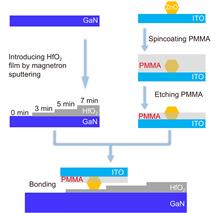
Interface emission from heterojunction is a shortcoming for electroluminescent devices. A buffer layer introduced in the heterojunctional interfaces is a potential solution for the challenge. However, the dynamics for carrier tunneling to control the interface emission is still a mystery. Herein, the low-refractive HfOInterface emission from heterojunction is a shortcoming for electroluminescent devices. A buffer layer introduced in the heterojunctional interfaces is a potential solution for the challenge. However, the dynamics for carrier tunneling to control the interface emission is still a mystery. Herein, the low-refractive HfO2 with a proper energy band configuration is employed as the buffer layer in achieving ZnO-microwire/HfO2/GaN heterojunctional light-emitting diodes (LEDs). The optically pumped lasing threshold and lifetime of the ZnO microwire are reduced with the introduced HfO2 layer. As a result, the interface emission is of blue-shift from visible wavelengths to 394 nm whereas the ultraviolet (UV) emission is enhanced. To regulate the interface recombination between electrons in the conduction band of ZnO and holes in the valence band of GaN, the tunneling electrons with higher conduction band are employed to produce a higher tunneling current through regulation of thin HfO2 film causing blue shift and interface emission enhancement. Our results provide a method to control the tunneling electrons in heterojunction for high-performance LEDs..
Opto-Electronic Advances
- Publication Date: Sep. 25, 2021
- Vol. 4, Issue 9, 200064-1 (2021)


Light-triggered interfacial charge transfer and enhanced photodetection in CdSe/ZnS quantum dots/MoS2 mixed-dimensional phototransistors
Ziwei Li, Wen Yang, Ming Huang, Xin Yang, Chenguang Zhu, Chenglin He, Lihui Li, Yajuan Wang, Yunfei Xie, Zhuoran Luo, Delang Liang, Jianhua Huang, Xiaoli Zhu, Xiujuan Zhuang, Dong Li, and Anlian Pan
Mix-dimensional van der Waals heterostructures (vdWHs) have inspired worldwide interests and efforts in the field of advanced electronics and optoelectronics. The fundamental understanding of interfacial charge transfer is of vital importance for guiding the design of functional optoelectronic applications. In this worMix-dimensional van der Waals heterostructures (vdWHs) have inspired worldwide interests and efforts in the field of advanced electronics and optoelectronics. The fundamental understanding of interfacial charge transfer is of vital importance for guiding the design of functional optoelectronic applications. In this work, type-II 0D-2D CdSe/ZnS quantum dots/MoS2 vdWHs are designed to study the light-triggered interfacial charge behaviors and enhanced optoelectronic performances. From spectral measurements in both steady and transient states, the phenomena of suppressed photoluminescence (PL) emissions, shifted Raman signals and changed PL lifetimes provide strong evidences of efficient charge transfer at the 0D-2D interface. A series of spectral evolutions of heterostructures with various QDs overlapping concentrations at different laser powers are analyzed in details, which clarifies the dynamic competition between exciton and trion during an efficient doping of 3.9×1013 cm-2. The enhanced photoresponses (1.57×10⁴ A·W–1) and detectivities (2.86×10¹¹ Jones) in 0D/2D phototransistors further demonstrate that the light-induced charge transfer is still a feasible way to optimize the performance of optoelectronic devices. These results are expected to inspire the basic understanding of interfacial physics at 0D/2D interfaces, and shed the light on promoting the development of mixed-dimensional optoelectronic devices in the near future..
Opto-Electronic Advances
- Publication Date: Sep. 25, 2021
- Vol. 4, Issue 9, 210017-1 (2021)
Review
Quantum photonics based on metasurfaces
Jun Liu, Mingqian Shi, Zhuo Chen, Shuming Wang, Zhenlin Wang, and Shining Zhu
From metamaterials to metasurfaces, optical nano-structure has been widely investigated for novel and high efficiency functionalities. Apart from the intrisinsic properties of composite material, rich capabilities can be derived from the judicious design of metasurfaces, which enable more excellent and highly integrateFrom metamaterials to metasurfaces, optical nano-structure has been widely investigated for novel and high efficiency functionalities. Apart from the intrisinsic properties of composite material, rich capabilities can be derived from the judicious design of metasurfaces, which enable more excellent and highly integrated optical devices than traditional bulk optical elements. In the meantime, the abundant manipulation abilites of light in the classical domain can be carried over into quantum domain. In this review, we highlight recent development of quantum optics based on metasurfaces, ranging from quantum plasmonics, generation, manipulation and appplication of quantum light to quantum vaccum engineering etc. Finally, some promising avenues for quantum optics with the help of optical metasurface are presented..
Opto-Electronic Advances
- Publication Date: Sep. 25, 2021
- Vol. 4, Issue 9, 200092-1 (2021)
An advanced III-V-on-silicon photonic integration platform
Yingtao Hu, Di Liang, and Raymond G. Beausoleil
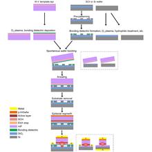
In many application scenarios, silicon (Si) photonics favors the integration of III-V gain material onto Si substrate to realize the on-chip light source. In addition to the current popular integration approaches of III-V-on-Si wafer bonding or direct heteroepitaxial growth, a newly emerged promising solution of epitaxIn many application scenarios, silicon (Si) photonics favors the integration of III-V gain material onto Si substrate to realize the on-chip light source. In addition to the current popular integration approaches of III-V-on-Si wafer bonding or direct heteroepitaxial growth, a newly emerged promising solution of epitaxial regrowth on bonded substrate has attracted a lot of interests. High-quality III-V material realization and successful laser demonstrations show its great potential to be a promising integration platform for low-cost, high-integration density and highly scalable active-passive photonic integration on Si. This paper reviews recent research work on this regrowth on bonded template platform including template developments, regrown material characterizations and laser demonstrations. The potential advantages, opportunities and challenges of this approach are discussed..
Opto-Electronic Advances
- Publication Date: Sep. 25, 2021
- Vol. 4, Issue 9, 200094-1 (2021)
© Copyright 2018-2021 | Chinese Laser Press. All Rights Reserved 沪ICP备15018463号-20