
Yingtao Hu, Di Liang, Raymond G. Beausoleil. An advanced III-V-on-silicon photonic integration platform[J]. Opto-Electronic Advances, 2021, 4(9): 200094-1
- Opto-Electronic Advances
- Vol. 4, Issue 9, 200094-1 (2021)
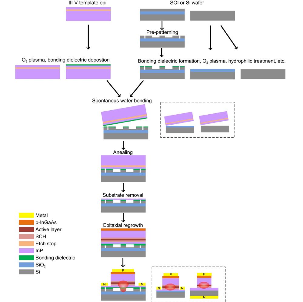
Fig. 1. A schematic drawing of the process flow for the advanced heterogeneous integration by using regrowth on III-V-on-Si bonding template.
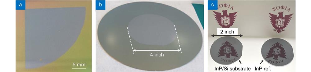
Fig. 2. Pictures of the fabricated InP-on-Si bonded wafers from HPE, III-V Lab and Sophia University. Figure repoduced with permisson from: (a) ref.29, under a Creative Commons Attribution 4.0 International License; (b) ref.31, (c) ref.25, John Wiley and Sons.
Fig. 3. Epitaxial regrowth laser structures on bonded templates from HPE, III-V Lab and Sophia University. Figure repoduced with permisson from: (a) ref.29, under a Creative Commons Attribution 4.0 International License; (b) ref.32, (c) ref.26, IEEE.
Fig. 4. AFM images and Nomarski microscope image of the epitaxial regrowth on bonded substrate from HPE, III-V Lab and Sophia University. Figure repoduced with permisson from: (a) ref.29,under a Creative Commons Attribution 4.0 International License; (b) ref.32, (c) ref.26, IEEE.
Fig. 5. Cross-sectional TEM (or STEM) images of the MQW or bulk epitaxy on the bonded substrate from HPE and III-V Lab. Figure repoduced with permisson from: (a, b) ref.29, under a Creative Commons Attribution 4.0 International License; (c) ref.32, IEEE; (d) ref.31, John Wiley and Sons.
Fig. 6. (a ) The electron channeling patterns corresponding to the three-beam (400) and (220) imaging conditions that were used in ECCI characterization. (b ) A representative ECCI image with only one TD. Figure repoduced with permisson from ref.29, under a Creative Commons Attribution 4.0 International License.
Fig. 7. The PL measurements at room temperature for the epitaxy on both InP and the bonded substrate from HPE, III-V Lab and Sophia University. Figure repoduced with permisson from: (a) ref.29, under a Creative Commons Attribution 4.0 International License; (b) ref.32, (c) ref.26, IEEE.
Fig. 8. XRD measurements on the epitaxy samples that from the three different research groups. Figure repoduced with permisson from: (a) ref.29, under a Creative Commons Attribution 4.0 International License; (b) ref.31, John Wiley and Sons; (c) ref.27, Elsevier.
Fig. 9. (a ) A microscope image of a FP laser with hybrid facets. (b ) Schematic drawing of the device cross-section and (c ) SEM of the hybrid facet. (d ) RT pulsed LIV. (e ) Pulsed LI up to 40 °C (inset: mode profile at facets). (f ) Device spetrum. (g ) cw LI up to 25 °C. Figure repoduced with permisson from ref.29, under a Creative Commons Attribution 4.0 International License.
Fig. 10. (a ) A microscope image of a FP laser with Si waveguide facets and a SEM image of a III/V-to-Si taper. (b ) RT pulsed LIV (inset: microscope image of the device), (c ) pulsed LI up to 40 °C (inset: mode profile at facets). Figure repoduced with permisson from ref.29, under a Creative Commons Attribution 4.0 International License.
Fig. 11. (a ) SEM image of the fabricated FP laser on InP-on-Si substrate. (b ) J-L characteristics in pulse injection mode at 20 °C: laser on bonded substrate (solid line) and the laser on InP (dash line). (c ) J-L characteristics in pulse injection mode measured at different temperatures for the laser on bonded substrate. (d ) Threshold current density evolution against temperature for the laser on bonded substrate (blue) and on InP (red). Figure repoduced with permisson from ref.32, IEEE.
Fig. 12. (a ) Measured lasing spectra of five FP lasers under C-W operation for a driving current of 100 mA at 20 °C. (b −d ) L-I characteristics under C-W operation for different temperatures for the lasers emitting at 1515 nm, 1580 nm and 1635 nm. Figure repoduced with permisson from ref.35, IEEE.
Fig. 13. (a ) A typical laser structure. (b ) The typical I-L characteristics of the MQW laser on the bonded substrate at various temperatures. (c ) A lasing spectrum for the MQW laser at an input current of J =6.83 kA/cm2. (d ) The temperature dependence of the threshold current density for the DH bulk lasers and MQW lasers on bonded substrates and on native substraes. Figure repoduced with permisson from: (a) ref.26, IEEE; (b, c, d) ref.27, Elsevier.
| |||||||||||||||||||||||||||||||||||||||||||||||||||||||
Table 1. A comparison of the main features in the demonstrations from the three research groups.
| |||||||||||||||||||||||||||||||||||||||||||||||||||||
Table 2. Qualitative comparison of production and operation costs of the same diode laser built on different III/V-on-silicon integration approaches.

Set citation alerts for the article
Please enter your email address
© Copyright 2018-2021 | Chinese Laser Press. All Rights Reserved 沪ICP备15018463号-20