• Journal of Semiconductors
  • Vol. 40, Issue 12, 122803 (2019)
Zhuohui Wu1、2、3、4, Jianchang Yan1、2、3、4, Yanan Guo1、2、3、4, Liang Zhang1、2、3、4, Yi Lu1、2、3、4, Xuecheng Wei1、2、3、4, Junxi Wang1、2、3、4, and Jinmin Li1、2、3、4
Author Affiliations
  • 1Research and Development Center for Solid State Lighting, Institute of Semiconductors, Chinese Academy of Sciences, Beijing 100083, China
  • 2Center of Materials Science and Optoelectronics Engineering, University of Chinese Academy of Sciences, Beijing 100049, China
  • 3Beijing Engineering Research Center for the 3rd Generation Semiconductor Materials and Application, Beijing 100083, China
  • 4State Key Laboratory of Solid-State Lighting, Beijing 100083, China
  • show less
    DOI: 10.1088/1674-4926/40/12/122803 Cite this Article
    Zhuohui Wu, Jianchang Yan, Yanan Guo, Liang Zhang, Yi Lu, Xuecheng Wei, Junxi Wang, Jinmin Li. Study of the morphology evolution of AlN grown on nano-patterned sapphire substrate[J]. Journal of Semiconductors, 2019, 40(12): 122803 Copy Citation Text show less
    Plan-view SEM image of the NPSS.
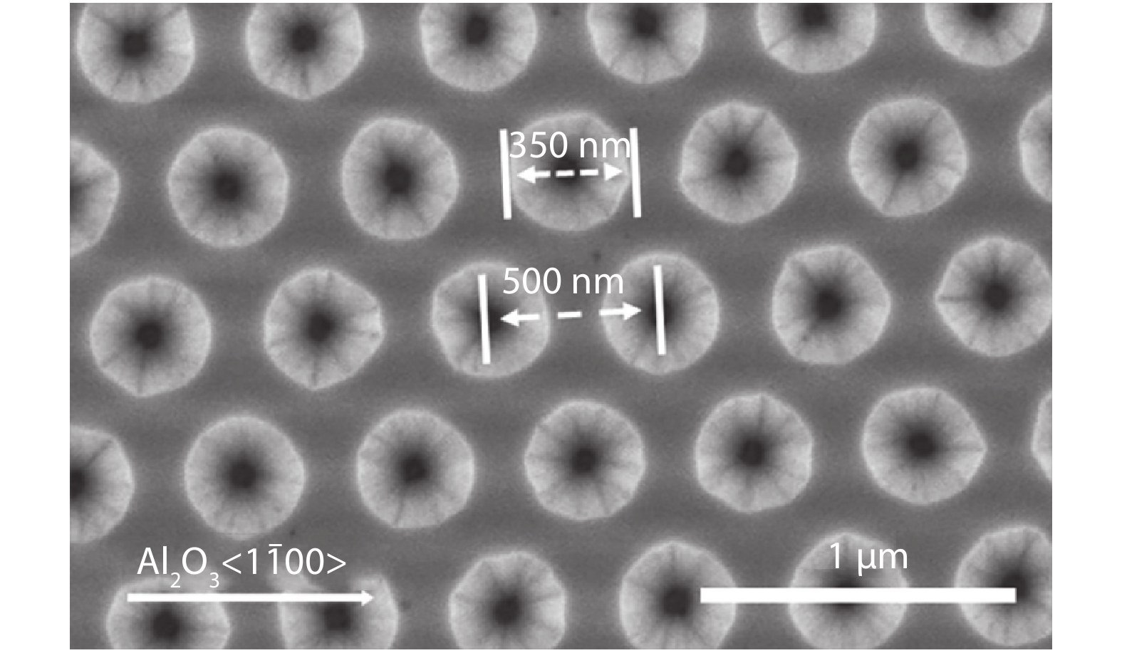
    Fig. 1. Plan-view SEM image of the NPSS.
    (Color online) Schematic diagrams of two samples with different structures.
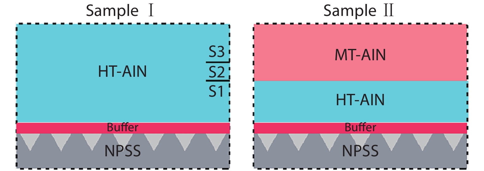
    Fig. 2. (Color online) Schematic diagrams of two samples with different structures.
    (a–c) Plan-view SEM images of surface morphology of sample I at end of the three growth stages. (d–f) The corresponding cross-sectional SEM images for (a), (b) and (c). The black dashed line in (a) indicates direction of the cross-sectional view as (d), (e) and (f). All images use the same scale bar as (a).
    Fig. 3. (a–c) Plan-view SEM images of surface morphology of sample I at end of the three growth stages. (d–f) The corresponding cross-sectional SEM images for (a), (b) and (c). The black dashed line in (a) indicates direction of the cross-sectional view as (d), (e) and (f). All images use the same scale bar as (a).
    Plan-view SEM images of surface morphology of Sample II.
    Fig. 4. Plan-view SEM images of surface morphology of Sample II.
    (a) 25° tilted-view SEM image of surface morphology of for as-grown MT-AlN. The inset shows cross-sectional view with the direction indicated by the black dashed line. (b) Schematic diagram of AlN growth keeping the 3D morphology. (c) and (d) Schematic of the AlN atomic structure.
    Fig. 5. (a) 25° tilted-view SEM image of surface morphology of for as-grown MT-AlN. The inset shows cross-sectional view with the direction indicated by the black dashed line. (b) Schematic diagram of AlN growth keeping the 3D morphology. (c) and (d) Schematic of the AlN atomic structure.
    (Color online) (a) Cross-sectional SEM image and (b) AFM image (2 × 2 μm2) of the Sample II after 2D growth.
    Fig. 6. (Color online) (a) Cross-sectional SEM image and (b) AFM image (2 × 2 μm2) of the Sample II after 2D growth.
    (Color online) Schematic diagram of the facet evolution of both samples.
    Fig. 7. (Color online) Schematic diagram of the facet evolution of both samples.
    Zhuohui Wu, Jianchang Yan, Yanan Guo, Liang Zhang, Yi Lu, Xuecheng Wei, Junxi Wang, Jinmin Li. Study of the morphology evolution of AlN grown on nano-patterned sapphire substrate[J]. Journal of Semiconductors, 2019, 40(12): 122803
    Download Citation