
Zhuohui Wu, Jianchang Yan, Yanan Guo, Liang Zhang, Yi Lu, Xuecheng Wei, Junxi Wang, Jinmin Li. Study of the morphology evolution of AlN grown on nano-patterned sapphire substrate[J]. Journal of Semiconductors, 2019, 40(12): 122803
- Journal of Semiconductors
- Vol. 40, Issue 12, 122803 (2019)
Abstract
1. Introduction
High-quality AlN template is essential to fabricate high-efficiency deep-ultraviolet light-emitting diodes (LEDs) and laser diodes (LDs), which can be widely used in sterilization, water purification, medicine, and biochemistry. Sapphire is one of the most suitable substrates for high-quality AlN template, thanks to its mature processing technique and high transparency in UV-light range[
Various patterns are selected to serve for the ELOG, such as stripe[
ELOG on concave patterned sapphire substrate can bring significant improvements for the crystal quality and device performance, which has reported by Dong et al.[
It should be noted that evolution of the facets might affect the evolution of the dislocation. For instance, with reference to the ELOG of GaN, the inclined facets arising in the process of coalescence play an important role in reducing the dislocation, as the threading dislocations which terminate at the inclined facets will bend in the basal plane during the lateral growth. Consequently, two steps ELOG of GaN including both 3D process which makes the surface contain as large inclined facets as possible and 2D recovery process was mentioned to improve crystal quality, which is called facet-controlled epitaxial lateral overgrowth (FACELO)[
In this paper, morphology evolution of AlN growth on NPSS under different growth conditions was detailly discussed and the growth habit of the
2. Experiment
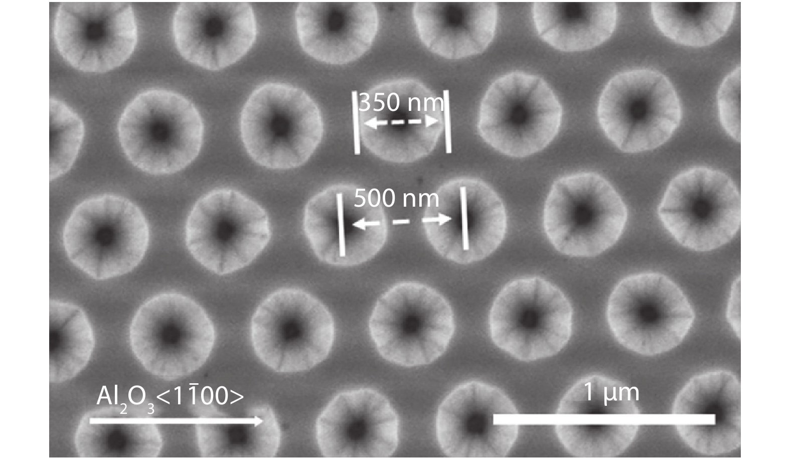
In this research, the NPSS was fabricated by nano-imprint lithography. As shown in Fig. 1, the opening diameter of circular hole is about 350 nm, and the period of the pattern is about 500 nm. A home-made low-pressure metal–organic chemical vapor deposition (LP–MOCVD) system with a vertical shower-head reactor was used to process epitaxial growth. Trimethylaluminum (TMAl) and ammonia (NH3) were used as precursors for Al and N, respectively. High-purity hydrogen (H2 )was used as the carrier gas. The reaction pressure was set as 50 Torr. Two samples with different structures were fabricated, as shown in Fig. 2, which manifested as different growth modes. The sample I contained the HT-AlN layers purely, which were grown at 1200 °C as normal growth temperature. The growth time for the HT-AlN in sample I was two hours, leading to near coalescence of the AlN epilayer. And the growth process of sample I was divided into three stages, which were labeled as S1 (0~40 min), S2 (40–60 min) and S3 (60–120 min), to investigate the evolution of the surface morphology. For sample II, an MT-AlN layer was grown based on the HT-AlN layer at 1130 °C. The growth time for the both HT-AlN layer and MT-AlN layer in sample II was 40 min. In addition, the V/III ratios of the HT-AlN and MT-AlN were 578 and 1156, respectively. Both samples were grown based on low-temperature buffer layer at 790 °C. The growth rate of HT-AlN and MT-AlN under the abovementioned growth condition was about 1.2 μm/h. After growth, scanning electron microscopy (SEM) and atomic force microscope (AFM) were used to study the surface morphology of the AlN.
![]()
Figure 1.Plan-view SEM image of the NPSS.
![]()
Figure 2.(Color online) Schematic diagrams of two samples with different structures.
3. Results and discussion
Fig. 3 presents the morphology of three distinguishing stages of Sample I. The corresponding growth time was 40, 60, and 120 min, respectively. At the initial stage, locally continuous AlN film with circular holes was gradually formed above un-etched mesa zones of the substrate after hundreds-nanometer growth. Then the outer contour of the holes turned into a hexagon shape when thickness of the AlN is around 800 nm, as shown in Fig. 3(a). Six inclined
![]()
Figure 3.(a–c) Plan-view SEM images of surface morphology of sample I at end of the three growth stages. (d–f) The corresponding cross-sectional SEM images for (a), (b) and (c). The black dashed line in (a) indicates direction of the cross-sectional view as (d), (e) and (f). All images use the same scale bar as (a).
As shown in Fig. 3(d), the value of θ is around 72°, thus the value of x is deduced to be ~1. According to the Wulff growth theory[
As shown in Figs. 3(b) and 3(e), the sidewall of the holes became vertical and the outer contour of the holes evolved to trapezium or triangle after totally 60 min growth. It illustrates that the six inclined facets are unstable. In addition, some misoriented AlN grew in the holes of sapphire substrate, as marked in the red dotted line circle in Figs. 3(a) and 3(d). Nevertheless, the misoriented AlN appearing in Fig. 3(a) is invisible in Fig. 3(b), deducing that continued growth of the misoriented AlN had been hindered when the inclined facets turned into vertical. As shown in Figs. 3(c) and 3(f), invert V-shaped air gap had been formed when the entire AlN film was nearly coalescent. The reason for the formation of the invert V-shaped air gap might be that the reactant which flowed into the holes was not sufficient for the growth of the lower part of the holes when the opening was small.
This process is quite different from GaN growth on the PSS. As for GaN[
Fig. 4 shows the evolution of facets for sample II. The typical morphology with six hexagonal inclined facets after HT-AlN growth for 40 min can be seen in Fig. 4(a). Continuing to react at the condition as HT-AlN will obtain the flat film, thus it can be called the 2D growth mode of the AlN. Conversely, the MT-AlN grown based on HT-AlN reveals no tendency of coalescence, as shown in Fig. 4(b). Growth front of the MT-AlN film is dominated by inclined facets, as the (0001) facet shrinks and even disappears. Thus the MT-AlN epilayer has 3D growth mode.
![]()
Figure 4.Plan-view SEM images of surface morphology of Sample II.
Fig. 5(a) shows the tilted-view SEM image of surface morphology after the growth of the MT-AlN, which has been already exhibited in Fig. 4(b). It reveals that the nanoholes with inverse pyramid morphology are well-arrayed. Each hole has nearly closed bottom and six inclined facets. From the cross-sectional SEM image, as shown in the inset of Fig. 5(a), the inclination angle of the facets was measured to be 58°, implying that the facets are
![]()
Figure 5.(a) 25° tilted-view SEM image of surface morphology of for as-grown MT-AlN. The inset shows cross-sectional view with the direction indicated by the black dashed line. (b) Schematic diagram of AlN growth keeping the 3D morphology. (c) and (d) Schematic of the AlN atomic structure.
Thus if the growth rate of the sloped gets smaller, point A will move left and top facet will shrink. So, the growth velocity of the
In addition, we also tried to realize 2D growth based on MT-AlN. The growth temperature was 1270 °C and the V/III ratio was 578. Flat surface had been obtained after the growth for 2 hours. As shown in Fig. 6(a), the total coalescence thickness was around 2.5 μm. Fig. 6(b) presents a 2 × 2 μm2 atomic force microscopy (AFM) image of the surface morphology of the sample II after 2D growth. AlN had a flat surface with a step-flow growth mode and a root-mean-square (RMS) roughness of 0.17 nm.
![]()
Figure 6.(Color online) (a) Cross-sectional SEM image and (b) AFM image (2 × 2
Another characteristic of the 2D growth based on MT-AlN is that two rows of air gaps in the coalescence region, as shown in Fig. 6(a). The phenomenon is different with typical ELOG of AlN as sample I, which was caused by the behavior of the
![]()
Figure 7.(Color online) Schematic diagram of the facet evolution of both samples.
4. Conclusion
We analyzed the morphology evolution of AlN grown on NPSS. We found the process that the
Acknowledgments
This work was supported by the National Key R&D Program of China (No. 2016YFB0400800), the National Natural Sciences Foundation of China (Grant Nos. 61875187, 61527814, 61674147, U1505253), Beijing Nova Program Z181100006218007 and Youth Innovation Promotion Association CAS 2017157.
References
[1] K Ding, V Avrutin, Ü Özgür et al. Status of growth of group III-nitride heterostructures for deep ultraviolet light-emitting diodes. Crystals, 7, 300(2017).
[2] A E Romanov, P Fini, J S Speck. Modeling the extended defect evolution in lateral epitaxial overgrowth of GaN: Subgrain stability. J Appl Phys, 93, 106(2003).
[3] M Imura, K Nakano, T Kitano et al. Microstructure of epitaxial lateral overgrown AlN on trench-patterned AlN template by high-temperature metal-organic vapor phase epitaxy. Appl Phys Lett, 89, 221901(2006).
[4] M Kim, T Fujita, S Fukahori et al. AlGaN-based deep ultraviolet light-emitting diodes fabricated on patterned sapphire substrates. Appl Phys Express, 4, 092102(2011).
[5] P Dong, J Yan, J Wang et al. 282-nm AlGaN-based deep ultraviolet light-emitting diodes with improved performance on nano-patterned sapphire substrates. Appl Phys Lett, 102(2013).
[6] D Lee, J W Lee, J Jang et al. Improved performance of AlGaN-based deep ultraviolet light-emitting diodes with nano-patterned AlN/sapphire substrates. Appl Phys Lett, 110, 191103(2017).
[7] Z Chen, R S Qhalid Fareed, M Gaevski et al. Pulsed lateral epitaxial overgrowth of aluminum nitride on sapphire substrates. Appl Phys Lett, 89, 081905(2006).
[8] K Nakano, M Imura, G Narita et al. Epitaxial lateral overgrowth of AlN layers on patterned sapphire substrates. Phys Status Solidi A, 203, 1632(2006).
[9] M Imura, K Nakano, G Narita et al. Epitaxial lateral overgrowth of AlN on trench-patterned AlN layers. J Cryst Growth, 298, 257(2007).
[10] J Mei, F A Ponce, R S Q Fareed et al. Dislocation generation at the coalescence of aluminum nitride lateral epitaxy on shallow-grooved sapphire substrates. Appl Phys Lett, 90, 221909(2007).
[11] R Jain, W Sun, J Yang et al. Migration enhanced lateral epitaxial overgrowth of AlN and AlGaN for high reliability deep ultraviolet light emitting diodes. Appl Phys Lett, 93, 051113(2008).
[12] H Hirayama, S Fujikawa, J Norimatsu et al. Norimatsu J, et al. Fabrication of a low threading dislocation density ELO-AlN template for application to deep-UV LEDs. Phys Status Solidi C, 6, S356(2009).
[13] V Kueller, A Knauer, F Brunner et al. Growth of AlGaN and AlN on patterned AlN/sapphire templates. J Cryst Growth, 315, 200(2011).
[14] V Kueller, A Knauer, C Reich et al. Modulated epitaxial lateral overgrowth of AlN for efficient UV LEDs. IEEE Photonics Technol Lett, 24, 1603(2012).
[15] A Knauer, V Kueller, U Zeimer et al. AlGaN layer structures for deep UV emitters on laterally overgrown AlN/sapphire templates. Phys Status Solidi A, 210, 451(2013).
[16] V Kueller, A Knauer, U Zeimer et al. Controlled coalescence of MOVPE grown AlN during lateral overgrowth. J Cryst Growth, 368, 83(2013).
[17] U Zeimer, V Kueller, A Knauer et al. High quality AlGaN grown on ELO AlN/sapphire templates. J Cryst Growth, 377, 32(2013).
[18] P Dong, J C Yan, Y Zhang et al. AlGaN-based deep ultraviolet light-emitting diodes grown on nano-patterned sapphire substrates with significant improvement in internal quantum efficiency. J Cryst Growth, 395, 9(2014).
[19] L Zhang, F Xu, J Wang et al. High-quality AlN epitaxy on nano-patterned sapphire substrates prepared by nano-imprint lithography. Sci Rep, 6, 35934(2016).
[20] T Y Wang, C T Tasi, K Y Lin et al. Surface evolution and effect of V/III ratio modulation on etch-pit-density improvement of thin AlN templates on nano-patterned sapphire substrates by metalorganic chemical vapor deposition. Appl Surf Sci, 455, 1123(2018).
[21] S Hagedorn, A Knauer, A Mogilatenko et al. AlN growth on nano-patterned sapphire: A route for cost efficient pseudo substrates for deep UV LEDs. Phys Status Solidi A, 213, 3178(2016).
[22] M Conroy, V Z Zubialevich, H Li et al. Epitaxial lateral overgrowth of AlN on self-assembled patterned nanorods. J Mater Chem C, 3, 431(2015).
[23] B Beaumont, V Bousquet, P Vennegues et al. A two-step method for epitaxial lateral overgrowth of GaN. Phys Status Solidi A, 176, 567(1999).
[24] K Hiramatsu, K Nishiyama, M Onishi et al. Fabrication and characterization of low defect density GaN using facet-controlled epitaxial lateral overgrowth (FACELO). J Cryst Growth, 221, 316(2000).
[25] K Horibuchi, N Kuwano, H Miyake et al. Microstructures of two-step facet-controlled ELO-GaN grown by MOVPE method — effect of mask geometry. J Cryst Growth, 237, 1070(2002).
[26] P Vennegues, B Beaumont, V Bousquet et al. Reduction mechanisms for defect densities in GaN using one- or two-step epitaxial lateral overgrowth methods. J Appl Phys, 87, 4175(2000).
[27] D Du, D J Srolovitz, M E Coltrin et al. Systematic prediction of kinetically limited crystal growth morphologies. Phys Rev Lett, 95, 155503(2005).
[28] C He, W Zhao, K Zhang et al. High-quality GaN epilayers achieved by facet-controlled epitaxial lateral overgrowth on sputtered AlN/PSS templates. ACS Appl Mater Interfaces, 9, 43386(2017).
[29] K Hiramatsu, K Nishiyama, A Motogaito et al. Recent progress in selective area growth and epitaxial lateral overgrowth of III-nitrides: Effects of reactor pressure in MOVPE growth. Phys Status Solidi A, 176, 535(1999).
[30] S Li, A Wang. GaN based nanorods for solid state lighting. J Appl Phys, 111, 071101(2012).
[31] L X Zhao, Z G Yu, B Sun et al. Progress and prospects of GaN-based LEDs using nanostructures. Chin Phys B, 24, 068506(2015).
[32] Y Tian, J Yan, Y Zhang et al. Formation and characteristics of AlGaN-based three-dimensional hexagonal nanopyramid semi-polar multiple quantum wells. Nanoscale, 8, 11012(2016).
[33] T Wunderer, M Feneberg, F Lipski et al. Three-dimensional GaN for semipolar light emitters. Phys Status Solidi B, 248, 549(2011).
[34] T Wunderer, J Wang, F Lipski et al. Semipolar GaInN/GaN light-emitting diodes grown on honeycomb patterned substrates. Phys Status Solidi C, 7, 2140(2010).

Set citation alerts for the article
Please enter your email address
© Copyright 2018-2021 | Chinese Laser Press. All Rights Reserved 沪ICP备15018463号-20