H. F. Mohamed, Changtai Xia, Qinglin Sai, Huiyuan Cui, Mingyan Pan, Hongji Qi. Growth and fundamentals of bulk β-Ga2O3 single crystals[J]. Journal of Semiconductors, 2019, 40(1): 011801
Search by keywords or author
- Journal of Semiconductors
- Vol. 40, Issue 1, 011801 (2019)
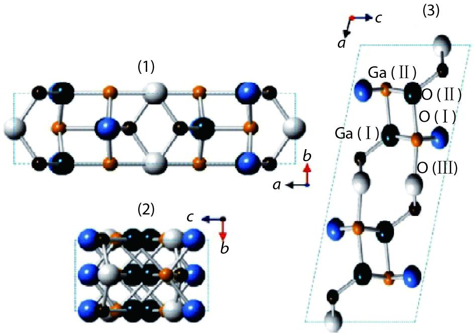
![(Color online) Unit cell of β-Ga2O3, which possesses two nonequivalent Ga sites: Ga (I), Ga (II), and three nonequivalent O-sites. Projection of the unit cell of β-Ga2O3 along the c- (A), a- (B) and b-axes (C). The figure was adopted from Ref. [9].](/richHtml/jos/2019/40/1/011801/img_1.jpg)
Fig. 1. (Color online) Unit cell of β -Ga2O3, which possesses two nonequivalent Ga sites: Ga (I), Ga (II), and three nonequivalent O-sites. Projection of the unit cell of β -Ga2O3 along the c - (A), a - (B) and b -axes (C). The figure was adopted from Ref. [9 ].
![(Color online) Electronic band structure of β-Ga2O3[15].](/richHtml/jos/2019/40/1/011801/img_2.jpg)
Fig. 2. (Color online) Electronic band structure of β -Ga2O3[15 ].
Fig. 3. (Color online) (a) Sketch of an early furnace used by Verneuil. (b) Simplified diagram of Verneuil process for synthesizing Ga2O3[16 ].
Fig. 4. (Color online) Schematic of float zone single crystal growth.
Fig. 5. (Color online) As-grown crystals along the crystallographic axis (a- <100>), (b- <010>), (c- <001>]).
Fig. 6. Schematic of Czochralski method.
Fig. 7. (Color online) Semiconducting β -Ga2O3 crystals of 2 cm (a, c) and 5 cm (b, d) diameter grown at low- (a, b) and high-oxygen concentrations (c, d)[25 ].
Fig. 8. (Color online) Edge-defined film-fed growth method.
Fig. 9. (Color online) (a) Photograph of EFG-grown β -Ga2O3 bulk crystal. (b) Photographs of processed β -Ga2O3 substrates. (c) 2-inch wafer by Electronic Material Research Institute of Tianjin. (d) 2-inch plate by Shanghai Institute of Optics and Fine Mechanics.
Fig. 10. (Color online) Bridgman technique.
Fig. 11. (Color online) β -Ga2O3 crystals were grown using the VB method in ambient air. (a–a’) Crystal was grown in a full-diameter crucible, and (b–b’) crystal was grown in a conical crucible. The figure was adopted from Ref. [38 ].
Fig. 12. (Color online) Schematics of line-shaped defects. The figure was adopted from Ref. [40 ].
Fig. 13. The comparison of the melt growth methods for β -Ga2O3 bulk single crystals.
Fig. 14. (Color online) Theoretical ideal performance limits of β -Ga2O3 power devices in comparison with those of other major semiconductors. The figure was adopted from Ref. [58 ].
Fig. 15. (Color online) Schematic illustration: (a) cross-section and (b) optical micrograph of Ga2O3 MESFET. According to the description from Ref. [62 ].

Set citation alerts for the article
Please enter your email address


